Note: Descriptions are shown in the official language in which they were submitted.
UK9-88-015 - 1 -
~2~-3~
DISPLAY SYSTEM
The invention relates to a display system comprising
a display memory for the storage of information for
display on a display device.
Many computer display systems in use today have both
an all points addressable (APA) display mode and an
alpha-numeric, or character, display mode. The APA
display modes are increasingly important as they allow
tex-t, graphics and image data to be displayed. Character
display modes (ie. using fixed-size character boxes)
while becoming less important, have advantages over APA
modes in certain circumstances (eg. for operating system
messages) because they intrinsically have less demand for
storage. Added to this, character display modes remain
necessary for reasons of compatibility with the large
number of alpha-numeric applications already existing.
As APA display modes are currently seen as the most
effective way of managing the display of computer
generated information, a lot of development effort has
been put into finding ways to improve the performance of
these modes. With this in mind, it has been suggested
that dual-ported display memory (in particular
dual-ported video memory which is otherwise known as
VRAM) should be used for the storage of data for display.
A VRAM is a particular form of dynamic RAM (or DRAM)
which, in addition to the usual DRAM random access mode,
has a serial access mode in which data can be output
sequentially at high speed in, for e~ample, an eight bit
wide data stream. This fast serial access to data stored
in a VRAM means that high video rate monitors can be
supported. However, the use of this technology poses a
problem when a display system also has to provide a
character mode, as the VRAM can only be accessed rapidly
if the data stored in the memory is accessed
sequentially. In a character mode, although the
accessing of the character code and attribute information
is se~uential, the accessing of the font memory is not,
UK9-88-015 - 2 - 2 ~ 2 ~
and thus the font cannot be usefully stored in the VRAM.
This problem is compounded in that prior display adapter
standards such as the IBMl Extended Graphics Array (EGA)
and the IBM Video Graphics Array (eg. VGA) which were
based on DRAM technology, allowed a large number of fonts
to be stored in their display memory, of which only a
limited number could be displayed on a display device at
any one time.
In a prior graphics standard (the IBM MCGA), a small
static store, separate from the display memory was used
for the storage of character fonts. However, only two
character fonts could be displayed (both of these being
held in the static RAM) with the result that MCGA
adapters are incompatible with the EGA and VGA standards
which require that more fonts can be dealt with.
European patent application EP-A-284,904 relates to
a display system with a symbol font memory in which a
selection of symbol fonts are stored in the system memory
of a workstation and only those portions of a symbol font
which are currently needed for display are transferred to
the display memory of a display system. In this way part
of the APA display memory is configured as a cache. This
prior display system addresses the system overhead
incurred in updating the display memory from the system
memory of the workstation, but does not address the
problem the instant inve~tion seeks to solve, namely the
efficient support of character modes in a display system
comprising a dual-ported display memory. Indeed, the
invention to which EP-A-284,904 relates is illustrated by
two e~amples, both of which are based on prior display
adapter standards which use DRAM technology; namely the
Colour Graphics Adapter (CGA) and the Extended Graphics
Array (EGA). It should be noted that the term "character
font" as used herein is intended to be synonymous with
the term "symbol font" used in EP-A-284,904.
1Registered trade mark
UK9-88-015 - 3 - ~Q21~31
An object of the invention is to provide a display
system having a dual-ported display memory for the
storage of information to be displayed, which display
system can efficiently support a character display mode.
In accordance with the invention, a display system
comprises a display memory for the storage of information
for display on a display device, said information
including character font definitions, a font cache for
the temporary .storage of the definitions of one or more
character fonts currently required for display and
control logic for updating the font cache from the
display memory.
Thus the invention provides, in addition to a
display memory, a separate font cache for the temporary
storage of currently displayable character (or symbol)
fonts. For a character display mode, the information for
display comprises character codes, character attributes
and font definitions for a plurality of different fonts.
Typically, the font definitions will define a large
number of different fonts. In a display system in
accordance with the invention, this information for
display is stored in the display memory. Especially in
the case where the display system also supports an APA
mode, there will be a relatively large amount of storage
which is needed for on-screen storage in the APA mode,
but which is available for off-screen storage in the
character mode. The on-screen storage re~uirements are
much higher in an APA mode.
It should be noted that although the primary object
of the invention is to enable a character mode to be
efficiently supported on a display system having a
dual-ported display memory for the storage of information
to be displayed, the invention would also be applicable
to display systems with display memories implemented in
other memory technologies.
~ UK9-88-015 - 4 - 2 ~ 31
The font cache is preferably in the form of
high-speed static storage. As only selected font
information is held in the font cache at any one time, it
may be relatively small. Preferably, in order to achieve
compatibility with existing display standards (eg. EGA,
VGA) two fonts are displayable at any one time.
In use, during active scan time the character codes
and attributes are accessed sequentially from the VRAM
and are passed to a serialiser which uses the character
codes to access the appropriate font information from the
cache. The serialiser then uses the font information
from the font cache with the attribute information for
creating appropriate video signals to drive the monitor.
During the vertical retrace period of the display,
however, neither the VRAM nor the font RAM are accessed
for the display purposes. During this time therefore,
the information defining the currently displayable fonts
can be accessed sequentially from the VRAM and written
into the cache. The contents of the cache can thus be
updated during successive vertical refresh times from the
fonts stored in the VRAM. Any individual change caused
by the system writing to the font area in VRAM or
changing the fonts currently selected for display is
reflected in the font cache within a few vertical scan
periods.
A particular example of a display system in
accordance with the present invention will be described
hereinafter with reference to the accompanying drawings
in which:
Figure 1 is a generalised block diagram illustrating
a typical configuration of a personal computer;
Figure 2 is a schematic block diagram illustrating
elements of a display system in accordance with the
invention;
UKg-88-015 - 5 - ~Q~1~31
Figure 3 is a schematic representation of the
content of the display memory of the display system of
Figure 2; and
Figure 4 illustrates a typical definition for a
character for display.
Figure 1 is a schematic block diagram of a typical
configuration of a workstation in the form of personal
computer such as one of the members of the range of IBM
PS/2 personal computers. The heart of the workstation
is a conventional microprocessor 10. This is connected
to a number of other units including a display adapter 12
via a system bus 14. Also connected to the system bus
are a random access memory RAM 16 and a read only store
18. An I/0 adapter 20 is provided for connecting the
system bus to the peripheral devices 22 such as disk
units . Similarly, a communications adapter 24 is
provided for connecting the workstation to a remote
processor ~eg. a mainframe computer). A keyboard 26 is
connected to the system bus via a keyboard adapter 28.
The display adapter 12 is used for controlling the
display of data on a display device 30. In operation the
CPU will issue commands to the display adapter over the
system bus for causing it to perform display processing
tasks.
The display adapter 12 illustrated in Figure
includes a display memory 36 for containing information
for display and logic for controlling display operations.
It should be noted however, that in some prior systems,
the display memory is formed by configuring part of the
system RAM 16. Either way, in prior computer systems,
the display memory is typically implemented using dynamic
random access memory (DRAM). Existing display adapter
standards such as the IBM Extended Graphics Array (EGA),
Trade Mark
UK9-88-015 - 6 - 2Q21~31
or the IBM Video Graphics Array (VGA) were designed to
make use of such a memory.
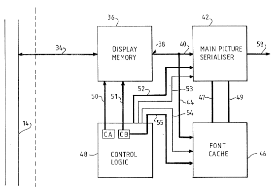
Figure 2 is a schematic diagram of elements of a
display system in accordance with the invention which is
configured as a display adapter 12 to be connected to the
system bus 14 of the personal computer in Figure 1 in
addition to, or as a replacement for the display adapter
12 shown in the Figure. For reasons of clarity, only
those details which are needed to explain the
implementation of the invention to one skilled in the art
are illustrated in Figure 2 and are described herein.
For example, features which may be included, but are not
described herein are buffers and/or memory control logic
in the path 34 between the system bus 14 and the display
memory 36 and a digital-to-analogue converter stage and
possibly a colour palette between the main picture
serialiser and the display device(s~ being driven by the
adapter.
Although a particular example of a "display system"
in accordance with the invention is described herein in
terms of the display adapter 12 for use in a workstation,
the term "display system" as used herein is not to be
limited thereto. The term "display system" is to be
interpreted to cover any system which is capable of
displaying information. Thus the workstation o Figure
1, when modified to incorporate the display adapter of
Figure 2, also forms a display system in accordance with
the invention. It should also be understood, that the
invention is not limited to the display of information by
means of a visual display monitor, but also includes the
display of inormation by means of, for example, a
printer.
The display adapter illustrated in Figure 2
comprises a display memory (sometimes otherwise known as
a refresh buffer or frame buffer) 36 composed of
dual-ported memory (here dual-ported video memory,
otherwise known as VRAM). The serial access port 38 of
2021~31
UK9-88-015 - 7 -
the VRAM is connected via a video path 40 to a main
picture serialiser 42. Data for updating the display
device are read out of the display memory via this serial
port and are passed via the video path 40 to the
serialiser 42. The serial output port of the display
memory is also connected via an additional path 44 to a
font cache 46. During periods when data is not required
for updating the display, data can be passed via the
additional path 44 for updating the font memory. The
serialiser is able to address the font cache via address
bus 47 for causing font data to be passed from the font
cache to the serialiser via data path 49. Control logic
48 is provided for controlling the operation of the
display adapter by means of address and control signals
passed via lines 50 - 55.
During the vertical retrace period of the display,
however, neither the VRAM nor the font RAM are accessed
for the display purposes. During this time therefore,
the information defining the currently displayable fonts
can be accessed sequentially from the VRAM and written
into the cache. The contents of the cache can thus be
updated during successive vertical refresh times from the
fonts stored in the VRAM. Any individual change caused
by the system writing to the font area in VRAM or
changing the fonts currently selected for display is
reflected in the font cache within a few vertical scan
periods.
In the present display adapter, which is for
supporting cathode ray tube type display devices, the
control lo~ic is implemented as part of the Cathode Ray
Tube Controller (CRTC~. In use, the CRTC causes data to
be read from the display memory in synchronism with the
scanning of the CRT display in accordance with the
current mode of operation (APA or character mode).
Before describing the operation of the display
adapter under the control of the CRTC, reference is made
to Figure 3 which is a schematic illustration of the
2021~31
UK9-88-015 - 8 -
content of the display memory in a character mode. Figure
3 represents the conceptual three dimensional structure
of a VRAM, with a number (here 8) bits of data per row
and column address. The VRAM memory itself is
conventional in construction and operation, so this will
not be described in detail. Briefly, however, the memory
can be operated using the normal (DRAM type) random
access port of the memory, and also using the fast serial
port of the VRAM memory. In the former case, specifying
a row and column address results in eight bits being
output from that location via the random access port.
When using the fast serial port of the VRAM however,
multiple sets of eight bits for consecutive memory
locations are output via the serial port starting from a
selected location in memory.
The character definition information is stored in
the on-screen portion of the display memory, starting at
a selected location CD in the memory (here location 0,0).
The "on-screen portion" of the display memory is scanned
sequentially during active display times for displaying
the data characters specified by the character definition
information stored therein. The definitions for a number
of fonts (typically eight) are also stored in the display
memory, although in an off-screen portion thereof. This
portion of the display memory is not scanned during
active display times. The definitions for the fonts each
start at a different memory location (Fl, F2, F3...).
The font definitions represent bit maps of each of the
characters of the font.
It will be apparent to one skilled in the art, that
the actual font data held in the memory will depend on
many factors (the actual font in question, the resolution
of the display, whether anti-aliasing and/or compression
techniques are employed and so on). However, each font
is stored with the data defining the bit maps for
respective characters of the font at successive locations
in the display memory.
2021~31
UK9-88-015 - 9 -
The character definition information for successive
characters to be displayed is stored sequentially in the
VRAM in which they are to appear on the display screen.
In this way, during the active display scan time, the
character definition information for successive
characters to be displayed on each display scan line can
be sequentially accessed in the VRAM.
A typical format for the character information for a
character is illustrated in Figure 4. It comprises a
character code, C, and attribute information, A. The
character code is used for specifying a particular
character within a font and the attribute information
selects between two fonts (bit F) and specifies the
foreground (bits FC) and background (bits BC) colours.
In use, the accessing of information from the
display memory is controlled by the CRTC. During active
scan times the character codes and attributes are
accessed sequentially from the VRAM and are passed to a
serialiser. The serialiser then assembles the video
information for controlling the display monitor from the
character information and font information. The
serialiser does not, however, take the font information
directly from the display memory, rather it obtains this
from the font cache.
Although the character definition information can be
stored such that it may~accessed from successive display
memory locations during active display times, the
character font information cannot be so stored. This is
partly because the order in which characters are to be
displayed on any particular line cannot be predicted in
advance, and partly because only one line of bit map data
for a character is needed for any one display line.
To illustrate this, consider a line of text to be
displayed which starts with the words "In the
beginning....". During the active display time for
scanning the first display line, the CRTC access the
UK9~88-015 - 10 - ~21~1
character codes for the characters "In the beginning...."
from sequential display memory locations. However,
assuming that the font data is stored in alphabetical
order, the character dot, or pixel information for those
characters will not be stored at sequential locations.
Thus for successive scan lines which make up a character
display line, the CRTC will cause access to the pixel
information for successive lines of the bit maps for
these characters in the order "In the beginning....". It
is assumed here that the display screen operates on a
non-interleaved raster scan. For an interleaved scan,
pixel data for half the scan lines need to be accessed
from the font during a first scan of the display screen
and pixel data for the other half of the scan lines,
which are interleaved between those of the first half,
need to be accessed during a second scan of the display
screen.
Given the above reguirements, and also that the
order of the characters for display on the next line of
characters will, in general, be different, it can be seen
that the font information for a character mode cannot be
accessed from sequential storage locations during active
display times.
For each scan line of the display, the serialiser
addresses the font cache via path 47 for accessing
appropriate pixel information for successive characters
to be displayed. The font cache addresses are generated
by serialiser from the font bit F and the character code
C for each character on that line as received from the
display memory via path 40 (this identifies the font and
character) and conventional display line count
information from the CRTC via path 52 identifying the
current scan line (this identifies the scan line within
the character). The pixel information is passed to the
serialiser via path 49 from the font cache. This pixel
information effectively specifies for each pixel position
on the display screen whether the background or
foreground colour specified in the corresponding
UK9-88-015 - 11 -
~021~31
character attribute information is to be displayed. The
serialiser uses this pixel information to gate the
appropriate colour information to the output line 58 for
driving the display monitor.
To obtain compatibility with existing display
adapter standards, the cache has the capacity to store
two complete fonts. For reasons of compatibility with
other existing display standards, eight fonts should be
held in the display memory. For meeting these
requirements, the font cache can be updated from the
display memory. This takes account of the fact that,
during vertical retrace neither the VRAM nor the font RAM
are accessed for the display purposes. The CRTC is
arranged, therefore to access the information defining
the currently displayable fonts sequentially from the
VRAM using the serial access port and to write this
information into the cache. The contents of the cache
can thus be updated during successive vertical refresh
times from the fonts stored in the VRAM. In this way,
any individual change caused by the system writing to the
font area in VRAM or changing the fonts currently
selected for display is reflected in the font cache
within a few vertical scan periods. It is possible to
update the font cache within this time thanks to the
speed of the VRAM serial port.
The mechanism for determining the destination of the
data from the display memory could take any suitable
form. Here, the destination is determined by the control
logic enabling the data inputs to the data serialiser and
the font memory at appropriate times via control signals
on control lines 53 and 54. During active display scan
times the data input to the serialiser is enabled via
control line 53 and the data input to the font cache
disabled. At times when update information is supplied
to the cache, the data input to the serialiser is
disabled, the data input to the font cache is enabled via
line 54 and address information is supplied to the font
cache by the CRTC.
UK9-88-015 - 12 - ~21$~1
If the available bandwidth does not permit the
content of the cache to be completely updated in one
vertical retrace period, the CRTC needs a separate
counting mechanism for addressing the display information
during active display times and a second counting
mechanism for addressing the font information for
updating the font cache. In the embodiment illustrated
in Figure 2, the CRTC includes a first counter CA for
counting from the base address CD to the final address
CDF at which the character definition information is
stored each time the display is refreshed. Figure 2
represents schematically these addresses being passed via
address lines 50 to the display memory. For addressing
the display memory during the updating of the cache (ie.
during non active display times) the CRTC includes a
second counter CB. This counter holds the position in
the font reached during each burst of font data supplied
during a vertical retrace time so that the updating of
the font may continue from that position during the next
vertical retrace time. Figure 2 represents schematically
these addresses being passed via address lines 51 to the
display memory. The content of the counter CB is used by
control logic in the CRTC as an index for generating not
only the display memory addresses from which font data is
to be read, but also the font cache addresses to which
data is to be written. Figure 2 represents schematically
these addresses being passed via address lines 55 to the
font cache.
The display system described above having a
combination of VRAM storage for the main storage of the
display information for a character mode and cache
storage for the temporary storage of currently
displayable font information provides the following
advantages:
- all access by the host system to the character,
attribute or font data can be to the VRAM which means
that they can have a high performance;
~ UK9-88-015 - 13 - 2 ~ 31
- all accesses to the character or attribute data by
the display system can be to the VRAM which means that
they can be sequential and that high video rates may be
supported.
- all accesses to the font data by the display
system can be to the cache;
- only a small cache is needed which means that it
may be made from high speed (static) memory and that high
video rates may be supported;
- fonts and other data can be stored exactly as they
were in previous adapters which means that register level
compatibility can be obtained; and
- the updating of the font cache can be achieved
during otherwise unused VRAM bandwidth so that system
performance need not be affected.
Although a particular e~ample of a display system
has been described, it will be understood that the
claimed invention is not limited thereto and many
modifications and additions are possible within the scope
of the claims.
For example, although the primary object of the
invention is to enable a character mode to be efficiently
supported on a display system having a dual-ported
display memory for the storage of information to be
displayed, the invention would also be applicable to
display systems with display memories implemented in
other memory technologies.
Also, although the font is only updated during
vertical display retrace in the above example, it could
be updated at any other time when display data is not
required from the display memory for display purposes.
For example, it could be arranged that the font cache
UK9-88-015 - 14 - 2~2 ~ 831
were also updated during horizontal retrace and/or
display blanking times.