Note: Descriptions are shown in the official language in which they were submitted.
2~219B~
ADAPTIVE POLARIZATION COMBINING SYSTEM
1 This invention was made with Government support.
The Government has certain rights in this invention.
, ,,'
BACKGROUND OF THE INVENTION
The present invention relates to electromagnetic
signal reaeiving systems, and more particularly to a
receiving s~stem wherein the polarization of the receive
antenna is matched to that of the incoming RF signal,
thereby maximizing the received signal-to-noise ratio.
In many instances, the polarization of the receive
signals is not known or may vary due to ionospheric
attenuation and reflection, multipath interference or
geometric relationship between the source and the receiv-
ing antenna. In certain instances, it is possible thatthe polarization of the signal at the source may be
varying for one reason or another.
Generally, the polarization of the receive antenna
is made to match to that of the incoming signal. However,
when the polarization of the receive signal is not known
or tends to change, a polarization diverse antenna is gen-
; erally used. This type of~antenna receives either two
orthogonal linearly or circularly polarized signals.~ For
the maximum reception o~ the incoming signal, these two
~rthogonally polarized components must be matched inrelative phase and amplitude to that of the incoming
signal. If only one component is used, which is generally
.,
''`' ~
.
: .
the case, no signal may be received if the received signal
polarization is orthogonal.
It is well known that any receive signal call be
decomposed into two linear components with certain relative
phase. In other words, a complete polarization match can
be made by adjusting the relative phas,e and amplitudes of
the two orthogonal linearly polarized signals. Schemes for ;~
matching the incoming polarization have been considered for
high performance space communication systems where signal
levels from deep space probes are often very marginal.
These schemes primarily have used mechanical polarization
adjustment systems. Although not directly related,
polarization mismatching schemes are used for adaptive
nulling the jammer signals. However, all of these schemes
do not require the polarization to be matched in very short
time without losing any information, that is, from pulse to
pulse.
SUMMARY OF THE INVENTION
It is therefore an object of an aspec~ of the
invention to provide a system which adaptively and
electronically adjusts the polarization of a receive ;i
antenna to match that of the incoming RF signal to maximize
the received signal-to-noise ratio.
An object of an aspect of the invention is to provide ~ -
an adaptive combining system which electronically adapts to
the polarization of the received ignal without any prior
knowledge or cooperation of the signal, and without losing
any signal information.
It is an object of an aspect of the invention to
provide an adaptive polarization combining system which
electronically adapts to the polarization o~ the received
signal, and operates over a wide instantaneous bandwidth
and can process a wide range of received pulse lengths from
CW to very short pulses.
The adaptive polarization combiner system in
accordance with an aspect of the invention Comprises a
~ : .
~' ;,.
._ ''
receive antenna, preferably a polarization diverse antenna
providing first and second output port signals which
comprise orthogonally polarized components o~ the incoming
signal. In a general sense, the antenna provides first and
second signal components of respective firsk and second
polarization senses.
The combiner system further comprises an adaptive
combiner circuit responsive to the first and second signal
components and comprising means for electronically adjust-
ing the phase and amplitude of the respective first andsecond component signals, and ~or combining the adjusted
signals at a single output port to polarization match the
system to the polarization of the received signal and to
maximize the signal-to-noise ratio of the output signal.
A calibration circuit is responsive to samples of the
first and second component signals to determine the
relative amplitude and phasing o~ the two component
signals. Calibration circuit signa}s dependerlt on the
relative amplitude and phase are then used to adaptively
adjust the combining circuit to the polarization of the
incoming signal
Other aspects of this invention are as follows:
An adaptive polarization combining system, comprising:
a receive antenna responsive to an incoming RF .signal
from a single source and having a first port for providing
received first component signals of a first polarization
sense of said incoming signal and a second port for
providing received second component signals of a second
polarization sense of said incoming signal;
means for providing time delayed versions of said
first and second component signals;
a calibration circuit responsive to said undelayed
first and second component signals and comprising amplitude
detecting means for detecting the relative amplitudes of
said first and second component signals and providing
amplitude detector signals indicative of said relative
amplitudes, and phase detecting m~ans for detecting the
.. ' '.
relative phase differential betw2en said first and second
component signals and providing a phase detector signal
indicative of said phase differential; and
an adjustable combiner circuit responsive to said
delayed versions of first and second component signals and
comprising means for electronically adjusting the phase and
amplitude of the respective delayed first and second
component signals and for combining the phase and amplitude
adjusted signals at a single combiner output port to
thereby polarization match the system to the polarization
of the received signal and maximize the signal-to-noise
ratio of the combiner output port signals, said combiner
circuit comprising means responsive to said amplitude
detector signals and said phase detector signals for
adjusting the phase and amplitude of said delayed versions
of said first and second sig~als without loss of
information or distortion of the received signal waveform.
A polarization~adaptive combining system, comprising:
a receive antenna responsive to an incoming RF signal
from a single source and having a first port for providing
received first component signals of a first polariæation
sense of said incoming signal and a second port for
providing received second component signals of a ~econd
polarization sense of said incoming signal;
means for providing time delayed versions of said
first and second component signals;
an adjustable combiner circuit responsive to said
delayed versions of first and second component signals and
comprising means for electronically adjusting the phase and
amplitude of the respective delayed first and second
component signals and for combining the phase and amplitude
adjusted signals at a single combiner output port to
thereby polarization match the system to the polarization
of the received signal without loss of information or
distortion of the received signals and maximize the signal-
to-noise ratio of the combiner output port signals, sai~
circuit comprising means for electronically equalizing the
phase of the delayed versions of said first and second
.
,. .: .
; , ; , ,, , . ,; . . , .. ~ . " .. , .,; ..
3b
component signals, first hybrid coupler means for receiving
as inputs said phase equalized delayed versions of said
first and second component signals and providing as first
and second hybrid outputs signals which are ~qual in
amplitude but have a phase differential dependent on the
relative amplitudes of the delayed versions of said first
and second component signals, means for adjusting the
relative phase of said first hybrid outputs, and second
hybrid coupler means having first and second input ports
and first and second output ports for combining the phase
adjusted first hybrid output signals so that substantially
all the power appears at said first output port of said
second coupler means as said combiner circuit output; and
a calibration circuit comprising a duplicate circuit
of said adjustable combiner circuit and responsive to said
undelayed first and second component signals, a phase
discriminator which receives as input signals the outputs
~rom the respective output ports of the second hybrid
coupler means of said duplicate circuit and provides a
first output signal proportional to the cosine of the phase
difference between the two input signals to the phase
discriminator and to the produce of the amplitudes of the
two input signals, and a second output signal proportional
to the sine of said phase diffsrence and to said produce,
and feedback means for controlling said means for adjusting
the relative phase of said first hybrid outputs of said
duplicate circuit by said first discriminator output
signal, and for controlling said means for adaptively
equalizing the phase of said first and second component
signals o~ said duplicate circuit by said second
discriminator output signal, said feedback means operating
in a closed loop fashion such that said phase discriminator
output signals are proportional to the errors in the
ad~ustments of said phase adjusting means and said phase
equalizing means.
An adaptive polarization combining system, comp~ising:
a polarization diverse receive antenna ~or reception
h`f a zignal of arbitrary polarization~ said antenna having
3c
a first port ~or providing received first component signals
of said signal of a ~irst polarization sense and a second
port for providing received second component signals o~
said signal of a second polarization sense, said first and
second senses being orthogonal to each other;
means for sampling said first and second component
signal to provide first port sample signals and second port
sample siqnals;
means for providing time delayecl versions of said
first and second component signals;
a calibration circuit responsive to said first and
second port sample signals and comprising amplitude
detecting means for detecting the relative amplitucles of
said first and second port sample siynals and providing
amplitude detector signals indicative of said relative
amplitudes, and phase detecting means for detecting the
relative phase differential between said ~irst and second
port sample signals and providing a phase detector signal
indicative of said phase differential, and
an adjustable combiner circuit responsive to said
delayed ~ersions o~ the first and second component signals
and comprising means for electronically adjusting the phase
and amplitude o~ the respective delayed versions of the
first and second component signals and for combining the
phase and amplitude adjusted signals at a single combiner
output port to thereby polarization match the system to the
polarization of the received signal without loss o~
information or distortion of the received signal and
maximize the signal-to-noise ratio of the combiner output
port signals.
BRIEF DESCRIPTTON OF THE DRAWINGS
These and other features and advantages of the present
invention will become more apparent from the following
detailed description of exemplary embodiments thereo~, as
illustrated in the accompanying drawings, in which~
.
~, "
.. j .
\
2 ~ 2 ~
1 FIG. 1 is a simplified schematic block diagram of a
combining circuit useful for polarization matching the
receive antenna to the incident RF signal.
FIG. 2 is a simplified block diagram of a receive
system employing an adaptive polarization matching circuit
in accordance with the invention.
FIG. 3 is a more detailed block diagram of the
receive system of FIG. 2.
FTG. 4 iS a schematic block diagram illustrative of
the amplitude detector comprising the calibration circuit
of FIG. 3.
FIG. 5 is a schematic block diagram illustrative of
the phase detector comprising the calibration circuit of
FIG. 3.
FIG. 6 is a schematic block d:Lagram of an alternate
adaptive polarization combining system.
DETAILED DESCRIPTION OF THE PREFERRED EMBODIMENT
A polarization diverse receive antenna generally has
a capability of receiving two linearly or two circularly
polarized signals. With appropriate phase and amplitude
adjustments of these two orthogonally polarized signals,
the polarization can be matched to that of the incoming
signal. Generally this process takes some finite -time and
may cause the receiver to lose some of the signals. To
circumvent any losses of these signals, a scheme is
required where any polarization matching is extremely
fast, that iSJ matching the phase and amplitude of the two
orthogonally polarized components adaptively. This
process must be fast enough so that no information i5 lost
in any communication waveforml no pulses are lost in radar
signals, and bandwidth must be sufficient to handle -~
frequency-hopping-type signals.
' .''~' :. '
- . .:
2 1~ 2 ~
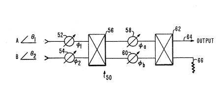
1 The basic concept of polarization matching to the
incoming signal is shown schematically in FIGo 1~ It is
assumed that a single signal source within the frequency
band o~ interest is incident on a polarization diverse
antenna having the two orthogonally polarized ports A and
B. The polarization diverse receive antenna system can
comprise, e.g., a dual polarized antenna such as a dual
circularly polarized antenna or dual orthogonal linear
polarization antenna structure. The signals at ports A
and B can have any relative amplitude and phase. Thus,
the signal at port A can be characterized as having an
amplitude A and a phase el. The signal at port B can be
characterized as having an amplitude B and a phase e2.
The combiner circuit 50 includes variable phase
shiters 52 and 54 for respectively shi~tlng the phase of
the signals at port A and por-t B by phase shifts ~1 and
02. The outputs of the phase shifters 52 and 54 are
connected to the inputs of a 90 hybrid coupler 56. The : -
two outputs of the hybrid coupler 56 are in turn connected i
to the respective inputs of a second 90 hybrid coupler 62
through variable phase shifters 58 and 60. The phase
shifters 58 and 60 vary the phase by respective phase ~`
shift values 0a and 0b. One of the outputs 64 of the
second hybrid coupler 64 is taken as the combiner circuit
output; the other output port is connected to a ma-tched
load 66.
By the use of the 90 degree hybrids 56 and 62 and
properly setting the phase shifters 52, 54, 58 and 60 it
is possible to get all of the combiner circuit output at
the desired output port 64 and none in the load 66. This
is done by setting the phase shift values 01 and 02 such
that the signals from ports A and B are in phase entering
the first hybrid 56. In that case, the two outputs from
the first hybrid 56 will be oE equal amplitude but have a
phase difference dependent on the relative amplitudes of
', - ' .
'
1 the incident signals at ports A and B. The two equal
amplitude signals are changed in phase by values 0a and 0b
through phase shifters 58 and 60 such that the signals
input into the second hybrid 62 are 9O degrees different
in phase, but still equal in amplitude. The second 9O
degree hybrid 62 will combine these two signals such that
all of the power appears at the output port and none at
the load port. In this case the signal at the output port
64 will be sum of the signal vectors of the fol:Lowing
magnitudes and angles: A/2(~01+0a) + A/2(el+01+~b-L80) -~
s/2~e2~02+0a-9 ) + B/2te2 02 b
It is possible to use only one of phase shifters 52
and 54 and/or only one of phase shifters 58 and 60, and
the choice of whether to use two, phase shifters will
depend on the specific hardware implementation.
The circuit 50 of FIG. 1 in general comprises a
means for adju~ting the relative phase of the port A and
port B signals 50 that they are in phase, and a variable
power combiner/divider circuit for combining the equal
phase signals and providing signals split between the tw~
output ports of the output hybrid. The polarization
diverse antenna in conjunction with the combiner circuit
50, comprises an antenna system which can have an arbi-
trary polarization. In order to match the system to the
polarization of the incoming signal and to maximize the
signal-to-noise ratio of the combiner circuit, the circuit
50 is adjusted so that al:L the power of the equal phase
slgnals is sent to the circuit output port 64.
The combiner circuit from FIG. 1 is used in the
adaptive polarization combining system of FIG. 2. The
antenna system lOl has the two output ports A and B as
; described above. The A and B channels are pre-amplified
by respective preamplifiers 102 and 104 prior to process-
ing by the svstem lOO such that the signal-to-noise ~S/N)
ratio is maintained. Sample signals A' and B' are coupled
2~2~
7 ~
:
... .
1 off by the respective directional couplers 106 and 108 to
the calibration circuit 150. The main signals A, B are
mixed at mixers 110 and 112 with a local oscillator signal
to down convert the main signal to the one GHz region,
passed through respective delay lines 114 and 116 to delay
the main signals to allow time for calibration, and the
phase and amplitude of the combiner circuit is adjusted by
the control signals from the calibration circuit. The
calibration circuit 150 outputs control the settings of
the phase shifters ;f52, 54, 58 and 60 of the combiner
circuit 50 (FIG. 1~. The sample signals A' and B' could
alternatively be coupled off after down converting the
main signals. -
The calibration circuit 150 is shown more ully in ~;
FIG. 3. The calibration sample signals A' and B' are
input to respective 3 dB couplers 152 and 154. The
signals from respective outputs of the couplers 152 and
154 are connected to an amplitude detector circuit 156.
The amplitude detector circuit 156 accepts the two input
signals, and outputs respective signals on lines 158, 159
which are related to the amplitudes of the input signals.
The signals on lines 158, 159 are in turn used to set the
attenuation levels of the variable attenuator circuit 160
of the calibration circuit. The signals 157 and 155, also
output from the amplitude detector circuit 156, set the
values of the phase shifters 58 and 60 comprising the
combiner circuit 50. `
Depending on the relative amplitudes of the signals
A' and B', determined by the amplitude detector circuit
156, either the A' channel signal or the B' channel signal
will be attenuated so that the signals A" and B" which are
input to the phase detector 170 will be equal in ampli- -
tude. Only the larger of the A' or B' channel signals
will be attenuated in order to maximize the signal level
lnto the phase detector 170.
':
.:
,
,:, ., . ,, : ,, .. .. , :, .,,,;, ., .. :,.. ,. ", . ,, , .,. , , . . . , . ~ ~ . ~ .. .. .
2~2~9~
1 The balanced signals A" and Bl' enter the phase
detector 170 and the output voltages (invertecl and
noninverted) determine the amount the phase shifters 52
and 54 have to be adjusted in the main channel combiner
circuit 50. S~ttings of the phase detector values 0a~ 0b~
01' 02 (FIG. 1) for several exemplary cases are given
below.
~ "
Case 1. Signal A Channel Only (Signal B = O) ~-
1 0 ~ '
Ampl. Det. Maximum Voltage on Signal 157
(156) 0 = ~90~ 0b = ~90
Channel A' = Full Attenuation
Phase Det. Zero Voltage
(170) ~1 = ' 02 =
'',: '
Case 2. Signal B Channel Only (Signal A = O)
Ampl. Det. Zero Voltage on Signal 157
(156~ 0a = ' 0b
Channel B' = Full Attenuation
:'
Phase Det. Zero Voltage !' '
~170) 0a = ' 0b =
; Case 3. Signal A & B Channels - In Phase, Equal Amplitude
Ampl. Det. Midrange Voltage on Signal 157
(156) 0a = ~45' 0b = 45
. .
... .
2 ~1 2 ~
.
g
1 Phase Det. Zero Voltage
(170) 01 = ' 02 = `
Case 4. Signal A & B Channels, In Phas~e, A = .707~ ~
I .
Ampl. Det. About 39~ of Maxim~m Vol-tage on Slgnal
157 ,
(156) 0a = ~35 3' 0b = ~35 3
1 0 '` ''
Channel B' = Partial Attenuation (so
that A" = B ~
Phase Det. Zero Voltage ;
(170) 01 = ' 02
'
Case 5. Signal A & B Channels, Equal Amplitude, Unequal
Phase ~ 180
;~`
Ampl. Det. Midrange Voltaye on Signal 157
(156) 0a = ~45~ 0b = ~45
Phase Det. Maximum
(170) 01 = +90 ~ 02 = ~90
Case 6. Signal A 6 B Channels, Equal Amplitude, Unequal
Phase ~90
Ampl. Det. Midrange Voltage on Signal 157
(156) 0a = ~45~ 0b = ~45
Phase Det. ~ Voltage
~170) 01 = ~45' ~2 = 45
,~
: .
2~2~
, "
1 The couplers, hybrids, mixers, amplifiers, phase
shifters and simple logic circuits co]mprising the system
100 are of conventional design and need not be described
in further detail.
One of the components comprising the system 100 is
the delay line used as delay devices 114 and 116. Gen-
erally, ~oaxial cable delay lines can be used where delay -~
required is on the order of a few to a hundred nano-
seconds. If a much longer delay is required, SAW devices
can be considered. However, coaxial delay lines are
adequate for most applications -~
The calibration circuit 150 comprises the amplitude ~
detector 156, variable attenuator circuit 160 and phase -
detector 170. The basic operation of this circuit is to
Eirst determine the relative amplitude of the signals from
Channels A' and ~' via the amplitude detector 156. The
output voltage of the dekector 156 will be sent to the
variable attenuator 160 and to the combining circuit 50.
This output voltage may be used in an analog or digital
form to set the diode bias in the variable attenuator 160
or to set the appropriate bits for diode phase shifters 58
and 60. ;
The calibration circuit 150 must first determine the
relative amplitudes of signals A' and B' so that the
signals A" and B" can be made equal for phase comparison
by the phase detector 170. The amplitude detector 156
accepts two input signals A' and ~' and outputs signals
related to ~he relative amplitudes of these signals. One
implementation of the amplitude detector is shown in FIG.
4. The inputs A' and B' are square-law detected by the
diodes 156A and 156~ and low pass filters 154C and 156D. -~
The resultant filter ~outputs are proportional to th
square of the input amplitudes. These outputs are used to
control the varia~le attenuators directly, with the
channel A' signals sent to the coupler 162 comprising the
: "':': " "
,:
2 ~
;
1 variable attenuator 160, and the B' signal sent to the
coupler 164. The control voltage requixed at the second
pair of combiner phase shifters 58 and 60 for perfect
combining is given by the formula
V = -2tan 1(A/B)
where A and B are the amplitudes of the input signals and
are positive or zero numbers. This voltage is derived
from the detected signals by the divide circuit 156E, the
square root circuit 156F, and the two quadrant inverse
tangent circuits 156G. An inverted signal is also provid-
ed via inverter 156H for the other phase shifter of the
differential pair.
lS The variable attenuator circuit 160 comprises two
variable attenuator circuits; each is a non-reflective,
non~phase-shift PIN diode attenuator circuit. The A'
channel attenuator comprises an input 3 dB, 90 hybrid
coupler 162, a pair of matched PIN diodes 163 and 165 and
an output 3 dB, 90 hybrid 166. The B' channel attenuator `~
comprises the input 3 dB, 90 hybrid coupler 164, matched
PIN diodes 167 and 169, and the output 3 d~, 90 hybrid
168. The unused ports of the hybrids 162, 166, 164, and ;
168 are terminated in matched loads. The input coupler of
each attenuator circuit divides the signal equally to both
PIN diodes. When the diodes are zero-biased or reversed-
biased, they will appear as open circuits which permits
nearly all the signal to travel to the output hybrid
coupler where the dividecl signals are combined at the
hybrid output port. Any unbalance due to the diodes or
the circuit will end up at the matched load of the output
hybrid. When the PIN diodes are biased in the forward
direction, the diodes draw current, the diode resistance
decreases and the diodes absorb a portion of the signal
35 ; while reflecting some of the signal back ancl into the
`" ~ ~ :.'''
' ' '- :'
2 ~
12
1 matched load of the corresponding input hybrid. The
remainder of the signal is combined in the output port of
the output hybrid. Because the att~nuation is performed
by matched diodes there is no phase shift for any atten-
uation setting. If phase shifters are used in place ofPIN diode attenuators, the output power is divided between
the output port and the matched load of the output hybrid.
This, however, results in phase shift at the output power
depending on the phase shifter setting.
The phase detector 170 accepts two same frequency
input signals of equal amplitudel and outputs a voltage
proportlonal to the phase difference between the inputs.
Thus, the phase detector exhibits the following mathe-
matical relationship:
out ~0A ~B), -180~ (~A-0B) ~ 180
where 0A and 0B are the phases of the two input signals
and k is the constant of proportionality. One implemen-
tation of the phase detector 170 is shown in FIG. 5. The
inputs A", B" are split into a total of four signals by
the 90 hybrid coupler 172 and the 0 hybrid coupler 174,
which are compared in two double balanced mixers 176, 178
resulting in signals propor-tional to the sine and cosine
of the phase diference. The sine and cosine signals are
further processed by a four quadrant arctanyent Eunction
circuit 180 which yields the desired output. An inverted
siynal is also provided via inverter 182 for driving the
other phase shifter of the differential pair of phase
shifters 52, 54.
The combining circuit 50 of FIG O 1, which follows
the delay lines 114 and 116 of FIG. 3, consists of input
phase shifters 52 and 54, an input three dB, 90 deyrees
hybrid coupler 56, power dividing phase shifters 58 and
~60, and an output three dB, 90 degrees hybrid coupler 62.
~. '
2~2~g~ .
13 :
1There are pairs of phase shifters shown in FIG. 1 and in
FIG. 3, but only one phase shifter at the input and one
phase shifter in between -the hybrids are required. If one
phase shifter is used, the values wou]Ld just be doubled.
5For instance, instead of 01 = ~45 and 02 = ~45~ ~1 could
be set for -90 or 02 = +90 eliminating one or the other .;
phase shifters. .
The phase shifts 0a and 0b are used to divide the
signal from channel A and B appropriately, so that if the
10signals from A and B are in phase, the total signal will
all emerge at the output port 64 and none at the matched
load 66 of the output hybrid coupler 62. rrhe settings of
0a and 0b are determined only by the amplitude of signals
at port A relative to the amplitude of signals at port B.
15'rhis measurement is performed by the amplitude detector
156 in the calibration circuit.
The settings 01 and 02 of the input phase shifters
52 and 54 are determined by the relative phase of the
signals at ports A and B. These input phase shifters are
20adjusted appropriately so that the two signals A and B are
in phase when they enter the output hybrid coupler 62 of -:
the variable power divider.
An alternate calibration circuit 150' is shown in ..
FIG. 6. It has several differences compared to the
circuit 150 o FIG. 3, including simplicity, use of
feedback, and component matching. Because the calibration
circuit 150' is a simpler circuit, it is less expensive to ;.
build and is more reliable than the circuit of FIG. 3.
The use of feedback automatically corrects for component
30imper~ections and changes due to temperature and aging. : .-
Finally, because the calibration circuit 150' has a high
degree of commonality with the combiner circuit 50, the
common components can be easily matched, resulting in
decxeased errors between the calibra-tion and combining
35operations. .;
.
2 ~
14
1 The alternate calibration circuit 150' operates as
follows. The two input signals are ~pplied to a duplicate
of the combiner circuit 50', the duplicate comprising
phase shifters 202 and 204, couplers 208 and 212 and phase
shifter 210. The duplicate combiner has two outputs
available from the final hybrid coupler 212. These
outputs are applied to a phase discriminator 214 which in
turn has two outputs I and Q. The action of the phase
discriminator 214 is to generate two voltages I and Q
which are proportional to the errors in the settings of
the previous phase shifters 202, 206 and 210. The phase
discriminator 214 is a conventional device, which accepts
two input signals and produces two outputs, I and Q. The
I output is proportional to the cosine of the phase
difference between the two input signals, and the Q output
is proportional to the sine of the phase difference. The
outputs I and Q are also proportional to the product of
the two amplitudes of the two input signals. Thus, if
either input signal is zero, both I and Q outputs are
2Q zero. The voltage I is amplified and applied to the phase
shifter 210; the voltage Q is amplified by amplifier 216
and applied to phase shifter 202 and through inverter 204
to phase shifter 206. This forms feedback loops which
automatically adju~t the phase shifters for optimum
combining for any input polarization. The phase shiftex
settings are then transferred to the actual combiner
circuit 50' that then does the final combining. The
sample and hold circuits 218, 220 and 222 between the
calibration and combining circuits 150' and 50', con-
trolled by sample and hold controller 224, prevent thetransfer of noise into the comblner 50' as well as holding
the settings for the falling edge of a pulsed signal.
It is understood ~that the above-described embodi-
ments are merely~ illustrative of the possible specific
embodiments which may represent principles of the present
.
. :,
.
2~2~
1 invention. For example, the invention is not limited to
use with a receive antenna system which provide~ signal
components which are orthogonally polarized. While the
output signal is maximized in that case, benefits will be
obtained for any two independent antennas which are not of
the same polarization sense. Other arrangements may
readily be devised in accordance with these principles by
those skilled in the art without departing from the scope
of the invention.
,'
.
.;
. ~ . . . . . . . . . .. . . , ~ . . , , .. . ,. , ~ , .. ..... . ... .