Note: Descriptions are shown in the official language in which they were submitted.
20221 ~3
MODULATOR AND DEMODULATOR
FOR DATA TRANSMISSION SYSTEMS
BACKGROUND OF THE INVENTION
The present invention relates to a modulating and
demodulating device (hereinafter referred to as MODEM)
for data transmission systems, and more particularly to
a modem capable of automatically determining whether to
set the delay equalizer or not.
A data transmission system links a data processing
apparatus with a data input/output apparatus or data
processing apparatus together, located in distance from
each other, for the transmission of information between
them. For this purpose, a data transmission system is
composed of various transmission paths and transmitting
apparatuses. Data processing apparatuses and data input/
output apparatuses are collectively called data terminal
equipment (DTE). Data transmitting apparatuses in a data
transmission system are known as data circuit terminating
equipment (DCE). A MODEM, a typical example of DCE,
achieves reciprocal conversion between the signal
interfacing conditions between DTE units and those on
transmission paths.
Usually, a MODEM in such a data transmission system
is provided with a delay equalizer to compensate for
delay distortion, and sometimes group delay distortion,
- 2 - 2022 1 5~
to which the transmitted data may suffer on the transmission
path. Group delay distortion on a telephone line, used
as the transmission path between MODEM's opposite to each
other,variès in characteristic with the number of links
on the line and other factors. On an exclusive line, the
characteristic of group delay distortion is determined
when the line is laid, and basically is subject to no
major subsequent change. Therefore, the delay equalizer
is set by the installing technician at the time of
installing the MODEM on the basis of the group delay
distortion characteristic of the line which he determines
by an actual data transmission test using the MODEM.
In this setting procedure, the technician comparatively
observes the eye patterns on an oscilloscope or some
other precision instrument when the delay equalizer is
inserted on the line and when not. Based on the result
of this comparative test, the technician judges whether
or not the delay equalizer should be set.
However, the above described setting procedure for
the delay equalizer requires not only a precision
instrument such as an oscilloscope but also a skilled
technician for the installation work.
SUMMARY OF THE INVENTION
An object of the present invention, therefore, is
to provide a MODEM for data transmission systems, which
~ 3 ~ 2022 1 53
can automatically set the delay equalizer without requiring
any special measuring instrument or its operation.
Another object of the invention is to provide a MODEM
for data transmission systems, which requires no skilled
technician, i.e. which allows a lay user to readily
decide whether or not to set the delay equalizer.
A MODEM for data transmission systems according to
one aspect of the invention is provided with a delay
equalizer for receiving via a transmission path a trellis-
coded test signal transmitted from an opposite MODEM andcompensating for delay distortion on the transmission
path of the test signal. A first switch selectively
supplies the test signal, which is the output of the
delay equalizer, and the test signal entered via the
transmission path. A demodulator demodulates the output
signals of the first switch. A decision circuit assigns
the output signals of the demodulator to predetermined
signal point coordinates. The MODEM iS also provided
with a Viterbi decoding circuit for computing the branch
metric representing the distance between each assigned
point and receive signal point from the output signals
of the decision circuit and the demodulator, and figures
out the pass metrics of accumulated values based on the
computed branch metric. An arithmetic processing circuit
selects the maximum and the minimum of the branch metrics
from the Viterbi decoding circuit, and determines and
2022 1 53
outputs the difference between the selected maximum and
minimum as a difference signal. The MODEM is further
provided with a second switch for supplying the difference
signal determined by the arithmetic processing circuit
as a first difference signal corresponding to the pass
metrics when the delay equalizer is not set for the
transmission path and as a second difference signal
corresponding to the pass metrics when the delay equalizer
is set for the transmission path. A controller compares
the first and second difference signals supplied by the
second switch, and sets the first switch in a state not
to set the delay equalizer for the transmission path if
the first difference signal is greater than the second,
or sets the first switch in a state to set the delay
equalizer for the transmission path if the second
difference signal is greater than the first.
BRIEF DESCRIPTION OF THE DRAWINGS
The above and other objects and features of the
present invention may be fully understood from the
following detailed description and the accompanying
drawings in which:
FIG. 1 illustrates a preferred embodiment of the
invention;
FIGS. 2 to 6 are diagrams for describing the trellis
coder in FIG. l;
5 20?2 1 53
FIGS. 7 and 8 are diagrams for describing the
characteristics of the delay equalizer in FIG. l; and
FIGS. 9A to 9H illustrate decision patterns of the
decision circuit in FIG. 1.
In the drawings, identical numerals denote
respectively identical structural elements.
DETAILED DESCRIPTION OF THE PREFERRED EMBODIMENT
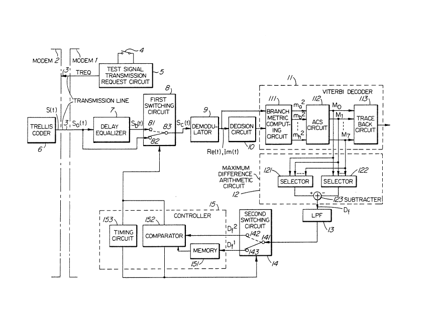
FIG. 1 illustrates a preferred embodiment of the
present invention with respect to a data transmission
system in which a first MoDEM 1 and a second MODEM 2
are connected to each other via a transmission path
(exclusive line) 3. Whereas the MODEM's 1 and 2 opposite
to each other are identical in configuration, FIG. 1
illustrates only the relevant parts of the system to
the two MODEM's in an arrangement in which the MODEM 1
is on the receiving side, and the MODEM 2 is on the
transmitting side, of a test signal needed for automatic
setting of a delay equalizer. In the MODEM 1, a starter
switch 4 is provided on the control board of the MODEM 1.
A test signal transmission request circuit 5 transmits a
transmission request signal TREQ for a test signal to the
opposite MODEM 2 via the transmission path 3 when the
switch 4 is turned on. Upon receiving the transmission
request signal TREQ sent from the request circuit 5 of
the MODEM 1 via the transmission path 3, the MODEM 2
- 6 - 2~22 1 53
prepares a trellis coding test signal S(t), and sends
this test signal to the opposite MODEM 1 via the
transmission path 3. Because of this procedure, the
MODEM 2 is equipped with a trellis coder 6.
Hereupon, the trellis coder 6 will be described
in detail. Trellis coding is a way of coding-for data
transmission, intended to increase the allowance for
noise on the line and improving the S/N versus error
rate characteristic. The trellis coder 6 for generating
a test signal having undergone this trellis coding
can have the configuration specified in the CCITT
Recommendation V.33. Referring to FIG. 2, the trellis
coder 6 consists of a differential encoder 61 and a
convolutional encoder 62. In this trellis coder 6, the
data to be transmitted are divided into six bits Q6n ...
Qln each, and inputted in parallel. Out of these six
data bits, four (Q6n~ Q5n~ Q4n and Q3n)
but only the other two (Q2n and Qln) are coded. The
differential encoder 61, as the truth table of FIG. 3
shows, compares the inputs Qln and Q2n with prior inputs
Yln 1 and Y2n 1' which are the previous outputs, and
sends out new outputs Y1n and Y2 . The operation of
this differential encoder 61 is similar to the differential
modulation system in the phase shift keying (PSK) system
and the quadrature amplitude modulation (QAM) system, by
which the data to be transmitted are converted into phase
- 2-022 1 53
variation quantities of the carrier signal and, although
an error arises at the moment of any instantaneous phase
variation due to a phase hit or the like, the subsequent
data are unaffected.
The convolutional encoder 62 subjects the outputs
Yln and Y2n of the differential encoder 61 to trellis
coding. A redundant bit YO is added in the convolutional
encoder 62, whose encoded outputs include three bits,
Y2n, Yl and YOn. This convolutional encoder 62 can
have eight different states according to the contents
Wnl, Wn2 and Wn3 of three delays (T). When there is
a change from one state to the next, the state into
which the change can take place is limited to one of
four out of the eight, and the change is governed by
the inputs Yln and Y2n. The state transitions possible
in eight-state trellis coding are shown in FIG. 4. For
instance, if the states Wnl, Wn2 and Wn3 are 000 at a
time n, the states W(n+l)l~ W(n+1)2 (n+1)3
time n+l will be one of 000, 001, 010 and 011. The
outputs of the convolutional encoder 62 are three bits
including the redundant bit YOn and inputs Yln and Y2n.
Since the redundant bit Yon at the time n is the same
as the content Wn2 of the delay, unaffected by the
inputs Yl and Y2 at the same time, the alternatives
of the outputs are limited to four out of the eight kinds.
As shown in FIG. 4, letters A, B, ..., H assigned to lines
- 8 - 2 22153
representing state transitions are the outputs in the
respective transitions. Thus, for the outputs Y2n, Yln
and YOn, A = 000, B = 010, C = 100, D = 110, E = 011,
F = 101, G = 111 and J = 001. For instance, when there
is the state of Wnl, Wn2 and Wn3 = 000, if 00, 01, 10
and 11 are entered as the inputs Yln and Y2n, each of
the transitional states W(n+l)l~ W(n+l)2 (n+1)3
will have the alternatives of 000, 011, 001 and 010.
At this time, the outputs of the convolutional encoder 62
will be 000 = A, 010 = B, 100 = C and 110 = D.
P 2n' Yln and Yon of the convolutional
encoder 62 and uncoded transmit data Q6n Q5n Q4n and
Q3n are arranged at 128 signal points in the signal space
shown in FIG. 5 according to the CCITT Recommendation V.33
in a mapping circuit 63. When, for instance, the inputs
to the mapping circuit 63 are Q6n/ Q5n/ Q4n/ Q3n/ Y2n,
Yln and YOn = 0101000, the signal points are arranged at
4 on the horizontal (P) axis and l on the longitudinal (Q)
axis. Therefore, the outputs P and Q of the mapping
circuit 63 will be P = 4 and Q = 1. The eight kinds of
outputs A, B, ..., H (each hereinafter referred to as
a subset) of the aforementioned convolutional encoder 62
can have 16 combinations corresponding to the 16
alternative states that the transmit data Q6n/ Q5n/ Q4
and Q3 can take. To indicate the signal points in
terms of the subsets A, B, ..., H, each point is
_ 9 2022 1 53
arranged according to a mapping rule illustrated in FIG. 6.
According to this rule, when the output of the convolutional
encoder 62 is the subset A for instance, 16 signal points
Ao to A15 are so mapped as to make the minimum distance
between them equal to 2~ times the minimum distance
between the 128 signal points. As a result, the data
error (error rate) characteristic with respect to line
noise is improved. The outputs P and Q of the mapping
circuit 63, i.e. the outputs of the trellis coder 6, are
subjected to QAM by a modulator (not shown), and sent
out to the transmission path 3 as a trellis-coded test
signal S(t) represented by Equation (1).
S(t) = Z sin (Wct) + P cos (Wct) ............. (1)
The delay equalizer 7 of the MODEM 1 shown in FIG. 1
receives via the transmission path 3 the trellis-coded
test signal S(t) sent out from the MODEM 2. The test
signal S(t), as it is affected by the group delay and
noise on the line constituting the transmission path 3,
is entered into the delay equalizer 7 as a test signal
Sa(t) represented by Equation (2). The equalizer 7
supplies a test signal Sb(t) having gone through
compensation for the group delay (equalization) on the
transmission 3 to which the test signal Sa(t) was subjected.
This test signal Sb(t) is represented by Equation (3).
Sa(t) = X1(t) sin (Wct + ~(t))
+ X2(t) cos (Wc + ~(t)) + n(t) ....... (2)
lO - 2022 1 53
Sb(t) = Xl(t) sin (Wct + ~'(t))
+ X2(t) cos (Wc + ~'(t)) + n'(t) (3)
where ~(t) and ~'(t) are phase errors;
n(t) and n'(t) are noises;
Xl is the output Q of the trellis coder, and
X2 is the output P of the trellis coder.
As an example of group delay on the line has the
characteristic shown in FIG. 7, equalization of the group
delay distortions by the delay equalizer 7 requires the
equalizer 7 to consist of a filter having the
characteristic shown in FIG. 8.
A first switching circuit 8 has a terminal 81 for
receiving the test signal Sb supplied by the delay
equalizer 7, a terminal 82 for receiving the test
signal Sa entered via the transmission path directly,
i.e. not through the equalizer 7, and a terminal 83
for selectively supplying the test signal Sb(t) fed to
the terminal 81 and the test signal Sa(t) fed to the
terminal 82. In this switching circuit 8, the selective
setting of a first state in which the terminal 82 and
the terminal 83 are connected or a second state in which
the terminals 81 and 83 are connected is controlled by
a controller 15 to be described below.
A demodulator 9 demodulates the signal Sc(t) ((Sc(t) =
Sa(t) or Sb(t)), and supplies signals Re(t) and Im(t).
The modulator 9 for QAM signals obtains a real part signal
11 - 2022 1 53
Re'(t) and an imaginary part signal Im (t), respectively
represented by Equations (4) and (5), by multiplying local
oscillation signals cos (Wct) and sin (Wct), having a
phase difference of ~/2 (90) between each other, and
the signal Sc(t).
Re'(t) = Sc(t) cos (Wct) ................... - (4)
Im'(t) = Sc(t) sin (Wct) ..................... (5)
These signals Re'(t) and Im'(t) are entered into a low-pass
filter (not shown) in the demodulator 9 to be cleared of
their quadratic harmonic contents. As a result, the
demodulator 9 supplies the real part signal Re(t) and
the imaginary part signal Im(t), respectively represented
by Equations (6) ~d (7), as information on receive signal
points.
Re(t) = 1/2X2(t) + n2(t) ......... (6)
S (t) = S (t)
Im(t) = 1/2Xi(t) + nl(t) ......... (7)
Re(t) = 1/2X2(t) + n2(t) ......... (6)
S (t) = Sb(t)
Im(t) = l/2Xl(t) + ni(t) ------ (7)
A decision circuit lO gives decisions on signal points
on the coordinates of the signals Re(t) and Im(tj, entered
from the demodulator 9, in ~ of the eight patterns A,
B, ..., H under the CCITT Recommendation V.33. FIGS. 9A
to 9H illustrate the eight decision patterns A, B, ..., H,
respectively. The coordinate positions of receive signal
points (x, y) represented by the signal Re(t) and Im(t)
are assigned to black dots (-) in the closest positions
- 12 - 2022 1 53
to the respective receive signal positions within the
borders marked with dotted lines. As the decision circuit
10 gives decisions on receive signal points in the eight
patterns, it outputs eight decision results (assigned
points) (X, Y). The transmit signal point of the test
signal S(t) supplied from the trellis coder 6 of the
opposite MODEM 2 is demodulated (reproduced) by the
demodulator 9, and the coordinates (P, Q) of this transmit
signal point correspond to the outputs (X2(t), Xl(t)) of
the demodulator 9. However, supposing the placement of
the spatial coordinates of the transmit signal point
and those of the receive signal point on the same scale,
X2(t) and Xl(t) of the signals Re(t) and Im(t) are
multiplied by 1/2 with respect to the signals P and Q
(see Equations (6) and (7)), so that the signals X2(t)
and Xl(t) should be multiplied by 2. The signals Re(t)
and Im(t) entered into the decision circuit 10 contain
noise including a phase error (~(t) or ~'(t)) content.
For these reasons, a receive signal point (x, y) usually
corresponds to the position of neither a black dot ( )
nor a white circle (o) on the coordinates of the decision
pattern, but typically exists in an x-marked position as
shown in FIGS. 9A and 9B. When a receive signal point
(x, y) is in an x-marked position ((Re, Im) = (4.5, 1.3)),
the decision circuit 10 assigns it to the black dot ( )
of (Re, Im) = (4, 1) in the direction pattern A (FIG. 9A)
- 13 - 2022153
and to that ( ) of (Re, Im) = (6, 3) in the decision
pattern B (FIG. 9B). Although any more specific description
is dispensed with here, the decision circuit 10 similarly
assigns the receive signal point (x, y) to the closest
black dot (-j within the same borders in every one of the
other decisions patterns C, ..., H.
The eight decision results (X, Y) obtained by the
decision circuit 10 in the decision patterns A, B, ..., H,
together with the signals Re(t) and Im(t), i.e. information
on the receive signal points (x, y), from the demodulator 9,
are entered into a branch metric computing circuit 111
which constitutes a part of a Viterbi decoder 11. The
branch metric computing circuit 111 subjects each of the
eight decision results to arithmetic operation.
m2 = (X _ x)2 + (y _ y)2 ..................... (8)
The arithmetic operation represented by Equation (8) gives
the square of the Euclidean distance between a decision
result (assigned point) (X, Y) and a receive signal point
(x, y). This makes it possible to find out branch metrics
m2 (m2 ma, mb, mc, ..., mh) for all the eight decision
results. To give specific examples, the decision results
(X, Y) and the receive signal points (x, y) in the
aforementioned decision patterns A and B, the branch
metrics ma and mb of the decision patterns A and B,
respectively, are:
- 14 - 2022 1 53
ma = (4 _ 4.5~2 + (1 - 1.3)2 = 0.34
mb = (6 _ 4.5~2 + (3 - 1.3)2 = 5.14
The eight branch metrics ma, mb, mc, ..., mh obtained
by the branch metric computing circuit 111 are entered
A 5 into an adding, comparing and selecting ~ circuit 112,
which constitutes a part of the Viberbi decoder 11. The
ACS circuit 112 performs the arithmetic operations
represented by Equations (9) on the basis of the branch
metrics ma, mb, mc, ..., mh and eight variables Mo~ Ml,
..., M7. The results obtained for Mo to M7 are called
pass metrics.
Mo = min (Mo * ma ~ Ml * md ~ M5 + mC ~ M4 + mb )
Ml = min (Mo + mb ' Ml + mc ~ M5 + md ~ M4 + ma )
M2 = min (Mo + md ~ Ml + ma ~ M5 + mb ~ M4 + mC )
M3 = min (Mo + mc ~ Ml + mb ~ M5 + ma ~ M4 + md ) '---(9)
M4 = min (M2 + mg , M3 + mf , M7 + me ~ M6 + mh )
M5 = min (M2 + mh ~ M3 + me ~ M7 + mf , M6 + mg2)
M6 = min (M2 + mf , M3 + mg , M7 + mh ~ M6 + me )
M7 = min (M2 + me2~ M3 + mh2, M7 + mg2~ M6 + mf2)
In more detail, the states being denominated state 0
(W 1' Wn2 and Wn3 = 000) and state 1 (Wnl, Wn2 and Wn3 =
(Wnl, Wn2 and Wn3 = 111) according to the
values of the contents Wnl, Wn2 and Wn3 of the delay in
the convolutional encoder 62 ( see FIG. 2) of the trellis
coder 6, the pass metrics Mo~ Ml, ..., M7 respectively
- 15 - 2 022 1 53
correspond to the states O to 7. To take up the pass
metric Mo in Equations (9) as an example, it can be
understood from the state transition diagram of FIG. 4
that the achievement of the state O requires one of the
states 0, 1, 5 and 4 to be immediately preceding. The
subsets corresponding to these states are A, D, B and C,
respectively. If the subsets, A, B, ..., H correspond
to the decision patterns A, B, ..., H and branch metrics
ma, md, mc and mb are accumulated into pass metrics Mo~
Ml, M5 and M4, what is the smallest in value is likely
to be the most probable in determining Mo~ so that the
least of the four values is selected. By computing Mo
through M7 in this manner, the pass metrics of all the
conceivable state transitions are computed.
The pass metrics Mo~ Ml, ... , M7 are the accumulated
values of the transmit signal sequence and the receive
signal sequence. Since the receive signal sequence
having the smallest accumulated value should be the
closest to the transmit signal sequence, a trace back
circuit 113 can find the result of decoding by tracing
back the smallest sequence of pass metrics Mo~ Ml, ....
M7. The output of the trace back circuit 113, which is
the decoded result of the test signal S (t), is not sent
out from the MODEM 1 when the switch 4 iS being operated.
The trace back circuit 113, through constituting a part
of the Viterbi decoder 11, is not directly related to
the demonstration of the present invention.
2022 1 53
- 16 -
The pass metries Mo/ Ml, ..., M7 obtained by the ACS
eireuit 112 of the Viterbi decoder 11 are entered into
both a maximum value seleetor 121 and a minimum value
seleetor 122, whieh are eonstituents of a maximum
differenee arithmetie eireuit 12. The maximum value
seleetor 121 eompares the values of the entered pass
metries Mo~ Ml, ..., M7 and seleetively outputs the
maximum value. The minimum value seleetor 122 eompares
the values of the entered pass metries Mo~ Ml, ..., M7
and seleetively outputs the minimum value. The maximum
and minimum values of the pass metries seleeted by the
seleetors 121 and 122, respectively, are subjected to
subtraction by a subtractor 123, which is another
constituent of the maximum difference arithmetic circuit.
A difference signal Df from the subtractor 123 of the
maximum difference arithmetic circuit 12 has a noise
content. A low-pass filter 13 is provided to smoothen
this difference signal Df.
A second switching circuit 14 has a first terminal 141
for receiving the differenee signal Df from the filter 13,
a seeond terminal 142 and a third terminal 143 both for
seleetively and distributively supplying the difference
signal Df entered into the first terminal 141. In this
second switching circuit 14, the selective setting of a
first state in which the first terminal 141 and the third
terminal 143 are connected or a second state in which the
- 17 - 2022 1 53
first terminal 141 and the second terminal 142 are
connected is controlled by the controller 15 to be
described below. This switching circuit 14, when set
in its first state, passes such a difference signal
(first difference signal) Dfl between the maximum and
minimum values of pass metrics as corresponds to the
test signal Sa(t) received in a state wherein the delay
equalizer 7 is not set for the line and, when set in
its second state, passes such a difference signal
(second difference signal) Df2 between the maximum and
minimum values of pass metrics as corresponds to the
test signal Sb(t) of the output of the delay equalizer 7
set for the line.
The controller 15 comprises a memory circuit 151,
a comparator 152 and a timing circuit 153. The memory
circuit stores the first difference signal Dfl from the
second switching circuit 14. The comparator 152 compares
the first difference signal Dfl read out of the memory
circuit 151 and the second difference signal Df2 from
the switching circuit 14. If the comparison shows the
first difference signal Dfl to be greater than the second
difference signal Df2, the comparator 152 supplies a
signal (logical high level signal) for setting the first
switching circuit 8 and the second switching circuit 14
in their respective first states.- If the comparison
shows the second difference signal Df2 to be greater
21~22 1 53
- 18 -
than the first difference signal Dfl, the comparator 152
supplies a first timing signal (logical low level signal)
for setting the first switching circuit 8 and the second
switching circuit 14 in their respective second states.
The timing circuit 153, when the switch 4 is operated,
supplies for a prescribed length of time a second timing
signal (logical high level signal) for first setting the
first switching circuit 8 and the second switching 14 in
their respective first states, and then outputs a signal
(logical low level signal) for switching the setting to
place the first switching circuit 8 and the second
switching circuit 14 in their respective second states.
The timing circuit 153, with the lapse of a prescribed
length of time after supplying the second timing signal,
places its output in a high impedance state. The
comparator 152 keeps its output in a high impedance
state while the timing circuit 152 is operating.
In ~udging whether the delay equalizer 7 should be
set for the transmission path (line) 3 of the data
transmission system described above, the installing
technician (or the lay user) would operate the switch 4
when the MODEM 1 is not transmitting data or at the time
of installing the MODEM 1. In response to the operation
of the switch 4, the test signal transmission request
circuit 5 sends out a signal TREQ to request the opposite
MODEM 2 to transmit a trellis-coded test signal S(t).
19 - 20221 53
The MODEM 1 receives the test signal S(t) via the
transmission path 3 from the MODEM 2 having received the
signal TREQ as the test signal Sa(t). In the MODEM 1,
the timing circuit 153 of the controller 15 sets the
first switching circuit 8 and the second switching
circuit 14 in their respective first states in synchronism
with the operation of the switch 4 and, after the lapse
of a prescribed length of time, switches the first
switching circuit 8 and the second switching circuit 14
into their respective second states. Therefore, the test
signal Sa(t) is first entered as the test signal Sc(t)
into the demodulator 9 not via the delay equalizer 7
but through the first switching circuit 8. Signals Re(t)
and Im(t) demodulated by this demodulator 9 are entered
into the decision circuit 10, which assigns them to
predetermined signal point coordinates (see FIGs. 9A
to 9H). The Viterbi decoder 11 decodes the output signals
of the decision circuit 10 and supplies the decoded data
of the test signal Sc(t). This Viterbi decoder 11, with
its branch metric computing circuit 111 and ACS circuit
112, computes branch metrics m2, mb, m2, ..., mh from
the output signals of the decision circuit 10, and figures
out the pass metrics Mo~ Ml, ..., M7 from these computed
branch metrics. In the maximum difference arithmetic
circuit 12 consisting of the maximum value selector 121,
the minimum value selector 122 and the subtractor 123,
- 20 - - ~o2~53
the subtractor 123 supplies the difference between the
maximum pass metric value outputted by the maximum value
selector 121 and the minimum pass metric value outputted
by the minimum value selector 122 as the difference
signal Df. The difference signal Df supplied by this
subtractor 123 is smoothened by a low-pass filter 13
and entered into the second switching circuit 14. Since,
at this time, the second switching circuit 14 is set in
its first state by the timing circuit 153, the entered
difference signal Df is stored in the memory circuit 151
as the first difference signal Dfl.
After the lapse of a prescribed length of time
following the reception of the test signal Sa(t) from
the MODEM 2, i.e. the length of time required for the
above described processing to store the first difference
signal Dfl into the memory circuit 151, the timing
circuit 153 sets the first switching circuit 8 and the
second switching circuit 14 into their respective second
states. Therefore, the next test signal Sa(t) received
from the MODEM 2 is entered into the demodulator 9 via
the delay equalizer 7 as the test signal Sc(t) (Sb(t) =
Sc(t)). The decision circuit 10, the Viterbi decoder 11,
the arithmetic circuit 12 and the filter 13 operate in
the same manner as when the test signal does not come
via the delay equalizer 7 to enter the difference signal
Df into the second switching circuit 14. Since this
- 21 - 2022 ~ 53
second switching circuit 14, as stated above, is set in
its second state, the entered difference signal Df is
outputted from the terminal 142 as the second difference
signal Df2.
As a result of the above described processing, the
difference between the maximum and minimum values of
the pass metric when the delay equalizer 7 is not inserted
on the line is stored into the memory circuit 151 of the
controller 15, and from the second switching circuit 14
is entered the difference between the maximum and minimum
values of the pass metric when the delay equalizer 7 is
inserted. The difference between the maximum and minimum
values of the pass metric is proportional to the error
rate, and it is generally known to those skilled in the
art that the greater this difference the higher the line
quality (the quality of communication signals). The
comparator 152 of the controller 15 compares the first
difference signal Dfl stored in the memory circuit 151
and the second difference signal Df2 entered from the
second switching circuit 14 and, when the second
difference signal Df2 is greater than the first difference
signal Dfl, supplies a signal for holding the first
switching circuit 8 and the second switching circuit 14
in their respective second states. When the first
difference signal Dfl is greater than the second
difference signal Df2, the comparator 152 supplies
- 22 - ?2 21 5 3
a signal for setting the first switching circuit 8 and
the second switching circuit 14 in their respective
first states. Thus the comparator 152 performs setting
control so as to increase the difference between the
maximum and minimum values of the pass metric by inserting,
or not inserting, the delay equalizer 7.
When the switch 4 is operated for restoration after
the completion of the series of operations, the transmission
of the test signal S(t) from the opposite MODEM 2 is
discontinued. After the delay equalizer 7 has been set
as described above, the first switching circuit 8 holds
on to its set state unless the setting is altered.
In the preferred embodiment described above, only
those constitutent elements of the MODEM ' S 1 and 2 which
are relevant to the description of the present invention
were referred to, and the unmentioned elements are the
same as the corresponding ones in usual MODEM ' s . The
first switching circuit 8 and the second switching
circuit 14 can consist of either electronic or mechanical
switches. Further, although the memory circuit 151,
the comparator 152 and the timing circuit 153 are the
constituent elements of the controller 15 in the foregoing,
they may as well be independent or integrated with some
other constituent elements. The memory circuit 151 can
be arranged on the side of the second terminal 142 of
the second switching circuit 14 instead of that of the
- 23 - 2 U22 1 53
third terminal 143 of same, in which case the switching
circuits 8 and 14 may be set first in their respective
second states by the output of the timing circuit 153
and later set in the first states.
Other alternatives and modifications to the above-
mentioned embodiment can be made within the scope of the
invention defined by the appended claims.