Note: Descriptions are shown in the official language in which they were submitted.
2~2~
: --1--
CLOS~D LOOP BUCRING FIELD SYSTEM
sackground of the Invention
; The present invention relates to the operation of
cathode ray tubes (CRT'S) and, more particularly, to
5 mitigating the degrading effects of an external magnetic
field upon the operation of a CRT. For purposes of this
application the degrading effects discussed concern the
convergence, purity and raster rotation of the CRT.
Existing CRT displays suffer intolerable display
10 degradation in the presence of even moderate external
~` magnetic fieldsO Magnetic shields, i.Q. the high
permeability housing, surrounding the CRT typically
provides adequate shielding against external magnetic
fields oriented orthogonal to the CRT viewing axis.
' 15 However, they provide very little shielding against
external fields oriented parallel to the CRT viewing axis.
` For monochrome displays, external magnetic fields aligned
'~ parallel to the CRT viewing axis rotate the raster about
k the center (zero deflection point) of the raster, causing
20 the corners of the rasters to be obscured by the bezel and
causing misregistration with the display and any bezel
reference points (e.g. map overlays, variable function key
switches with CRT displayed switch labels, etc.). Color
shadow mask (CSM) displays are even more susceptible to
25 external fields. In addition to raster rotation, CSM CRT
displays lose color purity, convergence, and suffer
¦ increased brightness variation due to the external
magnetic field induced beam landing errors.
It is known that the harmful effects of an external
30 electromagnetic field may be reduced by providing a
bucking field about the CRT. However, existing systems
fail to adequately segregate the remedial bucking field
from both the CRT display and the external field sensor.
Attempts to measure the external field and regulate the
35 bucking field have therefore been of limited success and
have resulted in interfering with the normal operation of
, . .. i ,, .- . ~ , - - ... .. , . . . ..... - . - . , . - - . .
2~22~ ~2
--2--
the display. In contemporary devices the remedial bucking
` field may operate to distort the CRT display, and/or may
be detected and interpreted so as to be indistinguishable
from the external field sought to be remedied.
5 Contemporary systems are further limited in that the
magnetic susceptibility of the CRT housing and sensor must
be taken into account in order to accurately determine the
strength and direction of the external field and generate
an appropriate remedial field. Variations in the
10 construction of the CRT and/or the sensor may
substantially impact assessments of the strength of the
~ external field and the appropriate bucking field.
! The present invention provides an apparatus and
c technique wherein the external field to be remedied is
15 detected at a location spaced from the bucking field to
facilitate segregation and accurate assessment of the
external field. Moreover, the measurement of the external
field is effected within the CRT shielding housing so that
the measured field is limited to that which is not
20 adequately shielded by the housing. Consequently, the
remedied bucking field will be limited to that necessary
to mitigate the effects of the external magnetic field
within the housing. The present invention therefore
provides an apparatus and technique which overcome
25 limitations of similar contemporary systems and readily
accommodates variations in the sensor and CRT
construction.
Summary of the Invention
A system for improving the operation of a cathode ray
30 tube (CRT) is disclosed whereby interference caused by
external magnetic fields is mitigated. The system
comprises a CRT having a CRT magnetic shield housing and
at least one electromagnetic field sensor disposed
adjacent to the inner surface of the CRT housing. Sensors
35 form to generate a reference magnetic field and to
generate a sensor output signal in response to the
"~
~,~2~
--3--
detection of both the reference field and an external
field as sensed within the housing. A bucking field coil
drive circuit is provided in electrical communication with
- the field sensor, the drive circuit being operative to
genexate a bucking field coil drive signal responsive to
the field sensor output signal. A bucking field coil is
disposed circumferentially about the CRT and is driven by
the bucking field coil drive signal. The bucking field
coil generates a bucking electromagnetic field in
10 opposition to the sensed external magnetic field, thereby
opposing and reducing the degrading effects of the
external magnetic field on the CRT display.
In the presently preferred embodiment the field
sensor comprises a plurality of "E" core sensors having
, 15 opened ends disposed in abutting contact with the CRT
shield inner surface. The sensor further comprises sensor
drive coil disposed about the center leg of the "E" core
and detector coils disposed about the outer legs of the
~; "E" core. The detector coils are preferably disposed in
20 series electrical connection. The sensor is preferably
formed such that the sensor output signal is minimal in
the absence of an external magnetic field. The bucking
field coil drive circuit includes a potentiometer for
setting a variable offset corresponding to the sensor
25 output in the absence of an external magnetic field. The
nulled sensor(s) output signal is attributed to an
external field, and result in the generation of a bucking
r. field to oppose the external field.
,rief Description of the Drawings
Figure la illustrates the construction of an
exemplary sensor formed in accordance with the pr~sent
invention;
' Figure lb illustrates the sensor drive signal applied
to the drive coils of the sensor illustrated in Figure l;
Figure lc illustrates a signal induced in the
detector coils of the sensors set forth in Figure la:
,~ t~, 2 I~J ~
--4--
Figure 2 is a simplified block diagram of a circuit
formed in accordance with the present invention;
Figure 3 is a cross-sectional view of a CRT
incorporating a pair of sensors such as that illustrated
in Figure la;
Figure 4 is a functional block diagram formed in
accordance with the present invention;
Figures 5a-c are top, side and front views,
respectively, of the magnetic shield incorporating a
10 bucking field coil in accordance with the present
invention;
Figure 6a illustrates the coil configuration of a
sensor formed in accordance with Figure la;
Figure 6b is a schematic representation of the sensor
15 coil configuration illustrated in Figure 6a;
; Figure 7 is a grapical representation of the measured
; output of the sensors illustrated in Figure la, when
applied to the inner surface of a CRT, as a function of an
external field;
~3 20 Figure 8 is a graph of the measured bucking field
coil current produced in accordance with the described
embodiment, as a function of the external field. The
three sets of data correspond to three orientations of the
external field relative to the CRT viewing axis;
Figure 9 is a schematic diagram of a sensor drive
circuit formed in accordance with the present invention;
and
Figures 10 and 11 are schematic diagrams of a sensor
output signal processing circuit formed in accordance with
30 the present invention.
Detailed ~ tion of the Presently Preferred Embodiment
The detailed description as set forth below is
intended merely as a description of the presently
preferred embodiment of the invention, and is not intended
35 to represent the only form in which the present invention
may be constructed or utilized. The description below
~ , , . ., . . ;. . . .. . . .. . ~ . : , . . . . . . , . .; ~ . : .
2~J2
--5--
- sets forth the functions in sequence of signals that are
affected by the invention in connection with the
illustrated embodiment. It is to be understood, however,
` that the same, or equivalent functions or signal sequences
may be accomplished by different embodiments that are also
intended to be encompassed within the spirit and scope of
~, the invention.
` It is to be understood that the present invention
comprises both a novel sensor design and system
; 10 configuration which, though independently useful,
cooperate in the present invention to achieve advantages
over the operation of contemporary devices. Figure
illustrates the construction of a sensor device in
accordance with the present invention. As shown therein
15 sensor 11 comprises a substantially "E" shaped core 13
provided with a center leg 15, and first and second
peripheral legs 17, 19, respectively. Sensor drive coil
21 is formed about the core center leg 15. Sensor
detector coils 23, 25 are disposed about peripheral legs
20 17, 19 respectively. An electrical sensor drive signal is
provided to the sensor drive winding 21 via sensor drive
port 27. The sensor detector coils 23, 25 are disposed in
series electrical connection and generate an output at the
sensor output port 29.
25As further shown in Figure 1 sensor 11 is disposed
such that the open end of the sensor, i.e. defined by the
lower face of sensor legs 15, 17 and 19, are disposed in
abutting relationship with inner surface 31 of CRT shield
1 30. The CRT viewing axis is typically substantially
¦ 30 parallel to the plane of surface 31.
In operation, a series of sensor drive signals of
alternating polarity are applied to sensor drive input
port 27. Representative sensor drive signals are
illustrated in Figure lb. An electromagnetic field is
35 generated as a result of the sensor drive pulse, with the
field direction being dependent upon the polarity of the
2~J?J'~ ~
-6-
sensor drive pulse. Figure la illustrates the field
patterns generated as a result of a positive sensor drive
pulse applied to sensor drive port 27. The application of
a negative pulse to sensor drive port 27 will result in a
field pattern of similar geometry, but opposite direction.
As further illustrated in Figure la, the sensor 11
operates to induce a field within the shield 30. As
illustrated in Figure l, the sensor drive signal 40
` generates an electromagnetic field. The electromagnetic
^ 10 field may be viewed as two magnetic circuits , Cir. 1 and
Cir. 2, which are ideally balanced in the absence of an
external field. The first circuit (C.) comprises the
magnetic path between the sensor drive coil 21 and
detector coil 23. The second circuit comprises the
s; 15 magnetic path between sensor drive coil 21 and detector
t, coil 25. In theory, the sensor output signal 50 is
9~ substantially zero in the absence of an external magnetic
field sensed within the CRT housing. That is, both
magnetic circuits develop substantially identical field
20 strength at the same rate, and the coils are connected
such that the currents induced in the coils substantially
cancel each other. In practice, however, the sensor
output signal, even in the absence of an external field,
is not zero due to factors such as unintentional air gaps
~` 25 between the core faces and the shield material and the
non-perfect flatness of the materials. The sensor output
signal 50 when no external magnetic field is present is
¦ shown in solid lines. Sensor output signal 50 is
generally a spiked signal, having a peak amplitude 51 and
30 followed by a decreasing amplitude portion 53. The
positive and negative peaks are substantially the same
amplitude.
In the presence of an external magnetic field the
peak amplitude of the positive and negative portions of
35 the sensor output signal will differ. The difference is
due to the fact that the external magnetic field, and the
2~2~ ~
--7--
field corresponding to the sensor drive signal, are
additive during a first portion of the sensor drive signal
(e.g. during the positive drive pulse) and subtractive
;`, during a second portion of the sensor drive signal (e.g.
during the negative drive pulse). The present invention
- operates to detect changes in pulse amplitude attributable
to the presence of the external magnetic field and to
' generate an output signal useful to create an appropriate
bucking field.
~: 10 The electromagnetic shield around the CRT represents
a low reluctance shunt path for magnetic field lines
,~ oriented along the CRT axis. Where the sensor drive field
~'/ is being aided by the external field (i.e. where both
sensor drive field and the external magnetic field are
15 additive) the sensed field is greater than the sensed
field in the absence of any external field.
The sensor drive coil 21 is driven by an alternating
polarity sensor drive pulse of sufficient volt-seconds to
saturate the shield material that forms a portion of the
20 magnetic path between the drive coil and the respective -
detector coils. As the shield material saturates, its
permeability decreases, increasing the magnetic reluctance
and decreasing the signal induced into the sensor detector
coils 23, 25.
¦ 25 When no external magnetic field is present to the
shield the signals induced into each of the sensor
detector coils are normally equal, resulting in a net zero
sensor output signal. In practice, the unintentional air
gaps between the "E" core faces and the shield material,
30 are not quite equal in both magnetic circuits, resulting
in a small but non-zero sensor output with no external
field. The smal1 non-zero sensor output is depicted by
the alternating polarity spiked pulses illustrated in
Figure lb. -
-
-8-
When an external magnetic field is aligned with the
CRT viewing axis, (parallel to the long dimension of the
"E" core), the external field will aid the driven sensor
field in one of the magnetic circuits and oppose the
other. The magnetic circuit that is aided by the external
field will saturate more rapidly than the circuit that is
opposed by the external field, resulting in more rapid
decrease in amplitude of the pulse induced in the output
; winding of the magnetic circuit aided by the external
lO field than the circuit opposed by the external magnetic
field. Consequently, a net output signal is developed
which represents both the non-zero output of the system
with no external field in combination with the response of
the sensor to the presence of the external field. As
15 described below the processing circuitry in electrical
communication with the sensor operates to distinguish the
~! two components in the net output signal and thereby
identify the output signal portion attributable to the
effect of the external magnetic field. The processing
20 circuitry then operates to generate a bucking field drive
signal, regulated by the sensor output component
attributable to the external field. The resulting bucking
field functions to oppose the external field as it exists
interior to the CRT. In the preferred embodiment the
25 processing circuitry functions to integrate the sensor net
', output signal sychronously with the drive signal to
develop the bucking field drive signal.
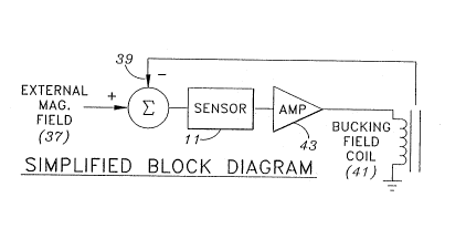
Figure 2 illustrates a simplified block diagram of a
bucking field system in accordance with the present
30 invention. As shown therein the sensor net output,
generally proportional to the field within the shield, is
nulled by the servo loop. The external magnetic field 37
is summed with a bucking coil field 39 produced by the
bucking field coil 41. The sensor ll, disposed within the
35 shield 30, operates to determine whether or not any
non-cancelled field results from the summing of the
2~?i~
g
bucking coil field 39 and the external magnetic field 37.
The sensor net output signal is communicated to amplifier
43 which scales the output of sensor 11 to an appropriate
drive signal which is communicated to the bucking field
coil 41. The circuit operates as a closed loop feedback
system such that the bucking coil field 39 is regulated to
mitigate the effect of the external magnetic field 37
within the CRT housing. The amplifier 43 includes
adjustments to calibrate the system (i.e., to null any
$ 10 circuit and sensor offset errors) for operation of the
system in the absence of an external magnetic field.
Thus, the system thereby avoids generating any responsive
buc]~ing field in response to the low level sensor output
attributable only to the characteristic operation of the
15 system.
Figure 3 illustrates a cross-sectional view of a CRT
incorporating a plurality of sensors such as that
illustrated in more detail in Figure 1. As shown in
Figure 3 the sensors 11 are disposed adjacent the inner
20 surface 31 of the CRT shield 30. Consistent with
contemporary CRT'S, deflection yoke 45 operates to
regulate the imaging of light signals on CRT 20. The "E"
core sensors 11 are located inside the CRT shield 30 to
decrease the sensitivity of the sensors to any transverse
25 external magnetic fields. The CRT shield functions to
both shield the sensors from external fields orthogonal to
the CRT viewing axis. Thus, the construction
suhstantially limits the generation of a remedial bucking
field, in response to the presence of a transverse field.
30 Consequently, the invention avoids the need to provide
additional shielding about the sensors for transverse
field components. The sensors are preferably located
sufficiently rearward from the deflection yoke 45 to avoid
inducing sensor noise into the deflection and/or
35 deflection signals into the sensor circuit.
~2~
--10--
As further illustrated in Figure 3, the invention
encompasses the use of a plurality of sensors disposed at
spaced locations along the inner surface 31 of CRT shield
30. The following circuit diagrams illustrate the use of
5 four sensors symmetrically distributed radially about the --
CRT viewing axis. The output signals of the individual
sensors may be averaged to form an error signal to drive
the bucking field coil amplifier 43 (Figure 2). Display
performance is thereby extended to substantially greater
10 levels of external fields. Moreover the use of a
plurality of sensors mitigates the effect of magnetic
field gradients occurring across the dimensions of the CRT
shield. Tests have indicated that, in the absence of the
ipresent invention, external fields parallel to the CRT
15 viewing axis can produce unacceptable levels of display
degradation when the external field strength is
approximately one oersted. With use of the present
invention acceptable display performance can be extended
to environments where the external field strength is
20 approximately five oersteds.
Figure 4 illustrates a functional block diagram of a
system formed in accordance with the present invention.
As shown therein the circuit includes four sensors which
are disposed about the CRT, as generally illustrated in
25 Figure 5c. Each of the sensors preferably comprise a
center-tapped (bifilar) coil, which serves to simplify the
generation of the dual polarity drive signals and the
parallel connection of the sensors to a single drive
source. Clock flip-flop 53 receives a clock input signal
30 which operates to permit clock drive circuit 51 to
alternately enable and disable transistors 55 and 57.
This construction results in simultaneously communicating
a sensor drive signal 40, of alternating polarity to each
of the sensor drive coils 21a, 21b, 21c and 21d. ~-
The detector coils of each sensor are represented as
coils 61a, 61b, 61c and 61d. Potentiometers 63, 65 and 66
2 ~
-11-
operate to gang the outputs of the sensor detector coils
and balance the outputs to effectively null out any system
imbalance in the absence of any external field, e.g.
imbalances due to magnetic field gradients about the CRT
viewing axis. Switch 69 operates to gate the ganged
output from detector sensors 61a-d to the bucking field
drive circuit 71 in coordination with the clock pulses.
; The output of switch 69 is communicated to sychronous
integrator 73 which is enabled during the clock pulse.
10 This sychronous integrator 73 reduces the effect of spikes
. . .
on the bucking field coil drive circuit 71, limiting the
response of the drive circuit 71 to the average value of a
detected signal. Potentiometer 75 is useful to null out
imbalances in the system as represented by the sensor
15 output signal in the absence of any external field. When
the sensor output exceeds a threshold amplitude level the
bucking field coil drive circuit 71 operates to generate a
bucXing field coil drive signal which is communicated to
bucking field coil 41. This causes bucking field coil 41
20 to generate an electromagnetic field about the CRT shield
which opposes the detected external field. Sensor drive
circuit 71 includes an amplifier circuit which
appropriately scales the sensor drive signal in relation
to the detected external field. The amplitude and other
25 characteristics of the sensor drive signal may be scaled
and modified in accordance with the particular environment
I of intended use.
Figures 5a, 5b and 5c provide top, side and front
views of the CRT incorporating features of the present
30 invention. Figure 5a illustrates sensors lla and llb
disposed about an inner rearward surface of CRT 30.
Bucking field coil 41 is shown disposed about CRT 30 at a
- location forward of the deflection yoke. Figures 5b and
5c provide further illustration of the positioning of the
35 sensor elements lla, llb, llc and lld, as well as the
bucking field coil 41.
.. ~
2~22162
-12-
Figures 6a and 6b illustrate one exemplary technique
for forming the "E" core sensor 11 and the appropriate
winding procedure. Figure 6a illustrates a pattern of
forming the coils about the sensor legs. In the
illustrated embodiment the coils 23, 21 and 25 each start
at the upper portion of legs 17, 15 and 19, respectively.
Figure 6b provides a schemtic representation of the wiring
pattern formed on the "E" core center.
The "E" core sensor has been formed using a core sold
10 by Magnetics, Inc., part number 44020EC. A layer of one
mil thick (0.001") mylar tape was formed about the legs of
the "E" core to protect the coils from abrasion against
t the "E" core ferrite material. #30AWG magnetic wire
(doubled) was used to form the coils. In the illustrated
15 construction two layers of coils were formed on the center
j leg. The first layer was formed by 23 turns of the
bifilar #30 wire. Thereafter the first layer was covered
with a layer of Mylar~ tape, leaving start and finish legs
outside of the tape for later connection. A second layer
20 of wiring was then formed about the center leg.
Twenty-one turns of the bifilar wire were used to form the
second layer. Upon completion of the second layer mylar
¦ tape was again wrapped around the wire. The left and
I right legs were each formed of 44 turns of wire, covered
1 25 with one layer of mylar tape. The wirings were connected
as illustrated in Figure 6b.
Pursuant to the construction illustrated in Figure 6a
and 6b, the magnetic parameters of the sensor were
determined to be as follows:
core:
Ae = 1.84 sq. cm
Le = 4.82 sq. cm
gsat = 4700 G
Al (EI) = 8150 mH/1000 sq. turns
shield:
Ae = (0.608 X 0.62) X (2.54 cm/in) = 0.243 sq.cm
~ .,.
2 ~
--13--
Lo = o.o52 X 8150 = 20.4 mH
Bsat = 15 kG
igure 9 is a schematic representation of the sensor
drive electronics, illustrating in more detail the
S circuitry set forth at Figure 4. As previously described
clock circuit 53 is operative to generate clock pulses
which are useful to both drive the sensors and to enable
the synchronize integrator. Sensor drive circuit 51
receives the clock pulses and generates sensor drive
10 signals. In the presently preferred embodiment the
sensors are implemented as center tapped transformers
alternating the polarity of the pulse drive signals.
Figure 10 is a schematic representation of the sensor
. .
; output signal processing circuit, shown more generally in15 Figure 4. Sensor output from the sensor coils 61a, 61b,
61c and 61d are ccmmunicated through an RC filter network
to potentiometers 63, 65, which serve as balance adjusts
for the top/bottom and left/right sensors, respectively.
Potentiometer 66 serves as a sensor diagonal balance
s 20 adjust. The balanced sensor output signal is then
3 communicated to transistor Q4, which is gated by the clock
CLK signal input to Q4. Sensor gain is regulated by
potentiometer 68. The gated sensor output signal is
' communicated to the synchronous integrator 73 which
25 smooths the operation of the system to avoid undesirable
responses to spurious signals. Potentiometer 75 serves as
an offset adjust to null out any error in the system due
to system non-zero response in the absence of an external
field. Thus, the present invention may be adapted for use
30 in conjunction with a variety of different CRT's. The
output from the synchronous integrator 73 represents the
drive to the bucking field coil (not shown) which
generates the opposing magnetic field to mitigate the
effects of the interfering field.
The output from the synchronous integrator may in
turn be amplified, as represented in Figure 11. The
2~2~2
-14-
amplification circuit shown therein, representing a
portion of amplifier circuit 71 (shown more generally in
Figure 4) utilizes the output from the synchronous
integrator to regulate a high current drive signal used to
5 drive the bucking field coil 41. The strength of the
~ bucking field coil current may be selected in accordance
1~ with a particular application. Moreover, the relationship
L between the sensor output and the strength of the bucking
field, linear or non-linear, may also be dictated by the
10 requirements of a particular application. For example,
it is anticipated that the CRT shield may exhibit
hysteresis characteristics that may require evaluation
prior to determination of the optimum bucking field
generated in response to different levels of external
15 field. Moreover, the frequency of the external field may
also impact the determination of the appropriate remedial
field. The presently preferred embodiment is directed to
a closed loop bucking field system suitable to remedy the
affects of a substantially constant externally magnetic
20 field. However, it is anticipated that other embodiments
may be usable to remedy alternating external magnetic
fields.
I