Note: Descriptions are shown in the official language in which they were submitted.
202235~
SUMMARY OF THE INVENTION
This invention deals generally with TV cameras and
more specifically with noise reduction in vertical
synchronization circuitry.
A common problem among vertical phase adjust circuits
is their susceptibility to power line noise. This is
particularly a problem with circuits which include
integrated circuit gate arrays because such gate arrays
generally operate on lower voltage signals so that they
are more sensitive to noise to which previous circuit
components were immune. Eurthermore, most vertical phase
adjust circuits have another deficiency in that they have
only a limited degree of phase adjustment. This limited
phase adjustment, typically about 300 degrees, may make
it difficult to exactly synchronize one camera with another.
The present disclosure solves both of these problems
by furnishing a vertical phase adjust circuit which is
adjustable for a full 360 degrees and also is highly immune
to line generated noise.
Essentially, the noise immunity is attained by
preventing the phase adjust circuit from generating another
output signal for an appreciable time after it has generated
an output. Since, for any given TV system, the period
between legitimate vertical synchronizing signals is fixed,
the present invention blocks all output signals from the
202235û
vertical phase adjust circuit for most of that period,
and thus produces a small "window" during which legitimate
delayed vertical output signals can be expected. In the
preferred embodiment the output signal is locked out for
approximately 98 percent of the period between legitimate
signals, thus reducing the likelihood of random noise
initiating a vertical synchronization signal to only two
percent of what it would otherwise be.
This operating window is created by using the
horizontal frequency generated within every TV system as
a basic timing signal. An integrated circuit ripple counter
is used to count horizontal periods after a vertical output,
and after a specific number of them, the circuit which
disables the output of the phase adjust circuit is itself
turned off. In the preferred embodiment, for a NTSC system
which has 262.5 horizontal periods within a normal vertical
period, the ripple counter is set for 256 counts. It is
these numbers which provide the lock-out ratio of 98
percent.
Such a lock-out circuit does, however, raise another
problem which the present arrangement also solves When
a TV system is first turned on the camera is, of course,
not immediately in synchronization with the system and
the small window provided by the lock-out circuit may not
be sufficient to permit initial synchronization. The
2022350
present disclosure, therefore, includes a circuit which
furnishes a larger synchronization window until the system
has become synchronized, at which time it changes to the
previously mentioned two percent window. This change in
the length of the lock-out time is accomplished very simply
by changing to a lesser count output on the ripple counter,
and for the preferred embodiment the change is to a lock-
out period of 128 horizontal periods. This changes the
signal window to approximately 50 percent of the vertical
period.
The present system also permits a full 360 degree
phase adjustment to facilitate the synchronization of the
camera to other cameras. Such a circuit must, however,
include provisions to assure that the phase adjustment
will not surpass 360 degrees, because phase adjustment
greater than 360 degrees would cause the camera to lose
synchronization with the system. The present disclosure
furnishes such a limiting circuit and does so with standard
integrated circuit components by ensuring that any given
vertical pulse is not delayed beyond the start of the next
vertical pulse.
This disclosure therefore furnishes a compact and
inexpensive vertical phase control system which not only
includes full 360 degree adjustment with provision to
prevent too great an adjustment, but also yields superior
~ 2022350
noise immunity and accommodates to the special synchronization
problems of system startup
Embodiments of the invention will now be described with
reference to the accompanying drawings wherein:
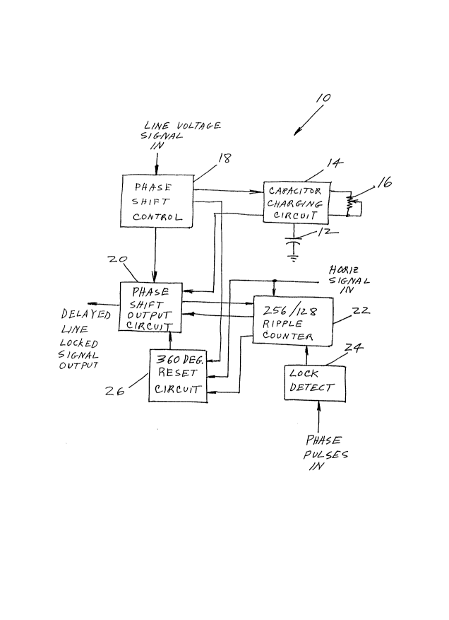
FIG. l is a simplified block diagram of the preferred
embodiment of the invention.
FIG. 2 is a more detailed circuit diagram of the preferred
embodiment of the invention.
DETAILED DESCRIPTION OF THE INVENTIVE EMBODIMENTS
The preferred embodiment of the invention is shown
in FIG. 1 in simplified block diagram form to better
introduce the basic circuit and its operation. In FIG.
1 vertical phase adjustment circuit 10 is composed of
capacitor 12 which is charged by capacitor charging circuit
14. The charging time of capacitor 12 is determined by
the setting of variable resistor 16. As is conventional
in most vertical phase adjustment circuits, it is the
charging time of capacitor 12 which determines the delay
for the vertical frequency of the TV camera within which
it is installed. In this circuit, as in most others, a
particular voltage level to which capacitor 12 becomes
charged triggers a switching device which discharges the
capacitor producing a sawtooth waveform. In the preferred
embodiment, the discharge switching device is a transistor,
and another transistor circuit, controlled by resistor
16, provides a linear charging rate for capacitor 12.
:0
2022350
The timing for the voltage charging capacitor 12
originates from the power line voltage being fed to phase
shift control circuit 18 which controls both the constant
current generator charging capacitor 12 and the transistor
discharging the capacitor.
The waveform produced by the charging and discharge
of capacitor 12 is fed to phase shift output circuit 20
where it triggers a flip-flop circuit to produce an output
pulse synchronized to the input line voltage but delayed
according to the setting of resistor 16.
As described to this point, the circuit is quite
conventional, but such a conventional circuit is clearly
susceptible to any noise signal which comes in on the line
voltage signal line. Any noise signal, such as that caused
by a motor starting on the AC line, can produce an erratic
and undesirable additional delayed vertical output signal
pulse The present circuity, however, virtually eliminates that
possibility.
As discussed above, this is accomplished with a lock-
out circuit which prevents output signals for all but the
very short time when the proper output signal is expected.
To do this the output from phase shift output circuit 20
also starts ripple counter 22 which counts the cycles of
the horizontal frequency of the system, and the output
of phase shift output circuit 20 is not cleared until the
2022350
ripple counter completes its prescribed count. This count
is typically set for 256, so that output circuit 20 is
not able to produce another output signal until 257 of
the usual 262.5 horizontal cycles in one vertical cycle
have been counted. False signals are therefore prevented
for approximately 98 percent of the operating time of the
circuit.
Unfortunately, when a system is first started and
the horizontal frequency generator is not stable, the
operating window open based on an unstable frequency is
not wide enough to assure that the system will synchronize,
so a circuit is included which will permit
synchronization at startup and at any other time that the
system might lose synchronization.
1S This circuit is lock detect circuit 24. It receives
the phase pulses signal from the vertical phase comparator
(not shown) within the TV system. The phase pulses signal
is present only when the vertical system is not synchronized
so it can be used to indicate the requirement for a larger
operating window. Lock detect circuit 24 processes the
phase pulses signal and controls ripple counter 22 to change
the count from 256 to 128. This decrease in the time for
which an output signal is locked out permits synchronization
in even the worst cases. Then, when synchronization is
established, the phase pulses signal stops and lock detect
-`- ` 2022350
circuit 24 re-establishes the higher count and the smaller
operating window.
The other additional circuit in the present system
is 360 degree reset circuit 26. In order to assure that
S the vertical phase adjust delay is not greater than the
maximum 360 degree adjustment and does not cause loss of
synchronization, 360 degree reset circuit 26 processes
a signal from phase shift control circuit 18 and counter
22 to determine when a 360 degree reset is necessary.
It then triggers output circuit 20 and restarts the charging
of capacitor 12 regardless o~ the state of phase shift -
control circuit 18.
FIG. 2 is a more detailed circuit diagram of the
preferred embodiment of the invention. It may be used
with the following description to better understand the
configuration and the operation of the various aspects
of the invention.
The line voltage signal fed to phase shift control
circuit 18 at flip-flop 30 is already clipped or attenuated
to the appropriate voltage of 0 to 5 volts. When this
input signal goes high, flip-flop 30-QN goes low, turning
on constant current capacitor charging circuit 14 and
linearly charging capacitor 12. When the voltage on
capacitor 12 reaches the threshold voltage of device 32
it will reset flip-flop 30, and 30-QN will go high. The
2022350
length of time it takes for capacitor 12 to reach the
threshold voltage of device 32 determines the vertical
phase delay. This time can be varied from several
microseconds to greater than 16.67 milliseconds by adjusting
resistor 16. The high voltage at 30-QN will turn off
charging circuit 14 and discharge capacitor 12 through
transistor 34. The high at 30-QN will also clock flip-
flop 36 sending 36-Q, which is the delayed line locked
output signal, high.
Once 36-Q goes high it is known that another valid
clock signal will not be present for 262.5 horizontal cycles
(when the system is using 60 Hz). Thus, if 36-Q is forced
to remain high for almost 262 horizontal cycles, another
clock pulse, whether false or not, will be disregarded.
To accomplish this, when 36-Q goes high, it enables a
counter 22 for which the clock frequency is the horizontal
camera frequency. When counter 22 reaches a count of 256,
flip-flop 38 is fed a high on 38-DA and the 257th clock
pulse will cause 38-Q to go high, resetting counter 22
and clearing flip-flop 36. Therefore, 36-Q is low again
and is ready to be sent high by the next line locked pulse.
The numbers used in the preferred embodiment, 256
and 128 for the counter for a NTSC system with 262.5
horizontal cycles within a vertical cycle, are of course
subject to design choice, so that a higher number for the
20~2350
counter will improve the noise immunity even more.
When the camera is not synchronized, for instance
during startup, the horizontal frequency will not be exactly
15.75kHz as in normal operation, and if it is too much
less than 15.75kHz, the time it takes to count 256
horizontal cycles will exceed one vertical period. Under
these circumstances the delayed output signal would have
a frequency of only 30Hz instead of the proper 60Hz, and
the camera would never be able to synchronize. Lock detect
circuit 24 overcomes this problem.
Lock detect circuit 24 determines when the vertical
is not synchronized and then decodes counter 22 at a count
of 128 rather than at 256. When the camera becomes
synchronized, lock detect circuit 24 returns the count
decoding to 256.
The signal for lock detect circuit 24 is derived from
the phase pulses signal which is received from the vertical
phase comparator (not shown). The phase pulses signal
is low during the time an error signal is being applied
to the camera's voltage controlled oscillator (not shown)
and high when no error voltage is being applied. The phase
pulses signal is low-pass filtered to create the lock detect
signal.
Two conditions must be met by the lock detect signal.
They are (1) the lock detect signal must not go high until
- 2022350
the camera is thoroughly synchronized and (2) the lock
detect signal must go low as soon as possible if the camera
loses synchronization for any reason. Both of these
conditions are met if different time constants are used
for the charging and discharging of capacitor 40. This
is accomplished by placing diode 42 in parallel with one
of the charging resistors 44. Thus, capacitor 40 is charged
slowly through both resistors 44 and 46, but discharged
essentially through only resistor 46.
360 degree reset circuit 26 assures that the preferred
embodiment of the invention, while permitting full 360
degree vertical phase delay, does not surpass the 360 degree
limit and lose synchronization. The reset circuit consists
of AND gate 48, flip-flops 50 and 52, and shift register
54.
If flip-flop 30-Q is high because capacitor 12 has
not yet charged to the threshold voltage of device 32 and
flip-flop 36-QN is high because the operating window is
open, the output of AND gate 48 will be high. If this
condition persists to within one horizontal period before
the next line signal input will occur, then the 360 reset
circuit will be set by flip-flop 50-Q going high. When
the next line signal input does occur flip-flop 52-QN goes
low setting flip-flop 36 and resetting flip-flop 30. The
high at flip-flop 52-Q is then clocked at the horizontal
- 1 0 -
2022350
frequency through three bit shift register 54. When the
high reaches the second bit, a signal output is generated
to reset flip-flop 52 and to remove the reset and set on
flip-flops 30 and 36. Then when the high reaches the third
bit, a signal output is generated to trigger flip-flop
30 again allowing the constant current source to begin
charging capacitor 12, thus restarting the delay cycle.
It is to be understood that the form of this invention
as shown is merely a preferred embodiment. Various changes
may be made in the function and arrangement of parts;
equivalent means may be substituted for those illustrated
and described; and certain features may be used
independently from others without departing from the spirit
and scope of the invention as defined in the following
claims.
. ~.