Note: Descriptions are shown in the official language in which they were submitted.
- 1 2022~86
1 TITLE OF THE INVENTION
SCAN CONVERTER CONTROL CIRCUIT HAVING
MEMORIES AND ADDRESS GENERATOR FOR GENERATING ZIGZAG
ADDRESS SIGNAL SUPPLIED TO THE MEMORIES
BACKGROUND OF THE INVENTION
The present invention generally relates to a
scan converter control circuit having memories, and
more particularly to a circuit for controlling a scan
converter directed to reducing the bit rate of an image
signal. Further, the present invention is concerned
with an address generator which generates a zigzag
address supplied to memories of the scan converter.
As is well known, an image signal has a wide
frequency range. In order to transmit such an image
signal in digital form, it is necessary to reduce the
bit rate of the image signal. For this requirement, a
bandwidth compression coding is proposed which utilizes
the correlation between the spatial axis and the time
axis.
The power of an image signal concentrates on
the low frequency components thereof. From this point
of view, the bandwidth of the image signal is
compressed by an orthogonal transform coding in which
the image data is converted into frequency components.
Examples of the orthogonal transform coding are a
discrete cosine transform (DCT) coding, Hadamard
transform (H) coding and Fourier transform (FT)
coding.
In the discrete cosine transform, output data
Y is obtained by the formula, Y = CXCt, where X is
input data, C is a predetermined square matrix based on
the transform type and ct is the transposed matrix of
the square matrix C. In order to realize the
above-mentioned formula by using hardware, the
following procedures are required. Matrix data (8x8
pixel data) must be rearranged on the input and output
20225~6
sides of an operation unit. Matrix data which is
transferred in synchronism with a data input clock must
be input to the operation unit in synchronism with an
operation clock. Matrix data which is output from the
5 operation unit in synchronism with the operation clock
must be output in synchronism with a data output
clock.
Referring to FIG.1, there is illustrated a
DCT coding circuit which implements the above-mentioned
10 procedures required to realize the aforementioned
formula by hardware. Input data applied to the DCT
coding circuit is sent to an operation unit 82 via a
scan converter 81. The operation unit 82 executes a
predetermined operation procedure using coefficient
15 data read out from a memory 83. The calculation
results output by the operation unit 82 are sent to an
external circuit of the next stage via a scan converter
84.
Each of the scan converters 81 and 84 has two
20 memory planes (areas) and a controller (software). The
controller alternatively switches the two memory planes
and controls read and write addresses supplied to the
two memory planes.
FIG.2 is a diagram illustrating a memory
25 plane switching operation, a write operation and a read
operation. One of the two memory planes is input to 64
pixel data DT-IN in synchronism with a data input
signal XDIN (FIG.2-(A)). The 64 data DT-IN are written
into the memory plane in a writing order shown in
30 FIG.2-(B), that is, a receiving sequence in a vertical
scan. After the 64 data DT-IN are completely written
into the memory plane, the 64 data DT-IN are read out
from the plane in a read order shown in FIG.2-(C), that
is, an output order in a zigzag scan. The readout data
35 are indicated by DT-OUT in FIG.2-(A). On the other
hand, 64 data is input to the other memory plane in
synchronism with the next data input signal XDIN.
2022~86
- 3 -
1 Then, the write and read operations are carried out in
the same way as described above. With the
above-mentioned arrangement, it becomes possible to
rearrange successive input data.
The procedure for alternately writing input
data into the two memory planes of each of the scan
converters 81 and 84 is alternately switched in
accordance with the data input signal XDIN. The
procedure for reading out data from the memory planes
is carried out subsequently after the writing of input
data is completed. In this manner, the memory plane
switching procedure is independently carried out for
each of the two memory planes. Conventionally, the
memory plane switching procedure is realized by
software (program). In this case, a huge number of
steps are necessary to implement the memory plane
switching procedure. Thus, it is very difficult to
execute the memory plane switching procedure in real
time. As a result, it is very difficult to process
consecutive image data in real time.
SUMMARY OF THE INVENTION
It is a general object of the present
invention to provide an improved scan converter control
circuit in which the above-mentioned disadvantages are
eliminated.
A more specific object of the present
invention is to provide a scan converter control
circuit in which control of the scan converters is
implemented by hardware so that image data can be
handled at higher-speed in real time.
The above-mentioned objects of the present
invention are achieved by a scan converter control
circuit comprising:
first and second memories, each having a data
write mode and a data read mode which are selected in
response to a switching signal so that the first memory
2022~86
- 4 -
1 is in the data write mode when the second memory is in
the data read mode and the first memory is in the data
read mode when the second memory is in the data write
mode;
write address counter means, operably coupled
to the first and second memories, for generating a
write address which is to be alternately supplied to
the first and second memories and for generating a
write completion signal when the write address becomes0 equal to a predetermined count value;
read address counter means, operably coupled
to the first and second memories, for generating a read
address which is to be alternately supplied to the
first and second memories and for generating a read
completion signal when the read address becomes equal
to a predetermined count value;
data input control means, operably coupled to
the write address counter means, for enabling the write
address counter means in response to a data input
signal supplied from an external circuit and for
disabling the write address counter means when
receiving the write completion signal;
memory switching control means, operably
coupled to the first and second memories, for
generating the switching signal having a logic value
which is changed in response to the write completion
signal; and
data output control means, operably coupled
to the write address counter means, the read address
counter means and the first and second memories, for
enabling the read address counter means in response to
the write completion signal and for disabling the read
address counter means in response to the read
completion signal.
The aforementioned objects of the present
invention are also achieved by a scan converter control
circuit in which the aforementioned write address
^ - 5 - 2022586
1 counter means or read address counter means comprises:
first up/down counter means, having an up
count mode and a down count mode selectively specified
by a first instruction signal, for generating an X
address in an X direction of an n x n pixel block by
counting a clock signal and for generating a first
underflow signal when the X address becomes equal to
zero in the down count mode;
second up/down counter means, having an up
count mode and a down count mode selectively specified
by a second instruction signal, for generating a Y
address in a Y direction of the n x n pixel block by
counting the clock signal and for generating a second
underflow signal when the Y address becomes equal to
zero in the down count mode;
first comparator means, operably coupled to
the first up/down counter means, for comparing the X
address with (n - 1) and for generating a first
coincidence detection signal when the X address becomes
equal to (n - 1);
second comparator means, operably coupled to
the second up/down counter means, for comparing the Y
address with (n - 1) and for generating a second
coincidence detection signal when the Y address becomes
equal to (n - 1); and
control means, coupled to the first and
second up/down counter means and the first and second
comparator means, for initially loading an initial
value into the first and second up/down counter means,
setting one of the first and second up/down counter
means to the down count mode and setting the other one
of the first and second up/down counter means to the up
count mode and for disabling one of the first and
second up/down counter means during a next clock period
of the clock signal when the one of the first and
second up/down counter means generates a corresponding
one of the first and second underflow signals and
- 6 - 2022586
1 simultaneously interchanging modes of the first and
second up/down counter means.
BRIEF DESCRIPTION OF THE DRAWINGS
Other objects, features and advantages of the
present invention will become apparent from the
following detailed description when read in conjunction
with the accompanying drawings, in which:
FIG.1 is a block diagram of a DCT coding
circuit;
FIG.2 is a diagram illustrating a
conventional memory plane switching operation, write
operation and read operation, all of which are executed
in the DCT coding circuit shown in FIG.1;
FIG.3 is a block diagram of the general
structure of a scan converter according to a preferred
embodiment of the present invention;
FIG.4 is a circuit diagram of the structure
shown in FIG.3;
FIG.5 is a circuit diagram of a data input
controller and a memory switching controller shown in
FIG.3;
FIG.6 is a circuit diagram of a data output
controller shown in FIG.3;
FIG.7 is a diagram of possible state
transitions which occur in the scan converter according
to the preferred embodiment of the present invention;
FIG.8 is a timing chart illustrating the
operation of the scan converter shown in FIG.4 which
corresponds to the state transitions shown in FIG.7;
FIG.9 is a timing chart illustrating the
operation of the scan converter shown in FIG.4;
FIGS.10A, 10B and 10C are diagrams
illustrating a zigzag scan;
FIG.11 is a block diagram of a counter used
in the scan converter;
FIG.12 is a block diagram of a detailed
_ 7 2022~86
1 configuration of the counter shown in FIG.11;
FIG.13 is a diagram illustrating the
operation of the counter shown in FIG.12;
FIG.14 is a timing chart illustrating the
operation of the counter shown in FIG.12; and
FIG.lS is a circuit diagram of a controller
shown in FIG.12.
DESCRIPTION OF THE PREFERRED EMBODIMENTS
A description will now be given of a scan
converter control circuit according to a preferred
embodiment of the present invention.
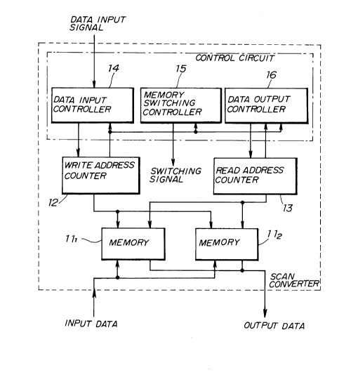
FIG.3 is a block diagram of the general
structure of a scan converter control circuit according
to the preferred embodiment of the present invention.
A scan converter 10 has a control circuit 20. A
plurality of memories (two memories in the structure
shown in FIG.3) 111 and 112 are alternately set to
a write mode and a read mode in accordance with a
switching signal generated and output by a memory
switching controller 15 provided in the control circuit
20. For example, when the memory 111 is in the write
mode, the memory 112 is in the read mode. A write
address counter 12 generates a write address and
outputs a write completion signal when the counter
value becomes equal to a predetermined count value. A
read address counter 13 generates a read address, and
outputs a read completion signal when the counter value
becomes equal to a predetermined count value. A data
input controller 14 in the control circuit 20 starts
the counting operation of the write address counter 12
in response to a data input signal which request to
input data, and stops the counting operation thereof in
response to the write completion signal. The memory
switching controller 15 inverts the logical value of
the switching signal in response to the write
completion signal so that the memory plane switching
- 8 - 2 0225~6
1 operation for the memories 111 and 112 is
realized. A data output controller 16 of the control
circuit 20 starts the counting operation of the read
address counter 13 in response to the write completion
signal, and stops the counting operation thereof in
response to the read completion signal.
In response to the data input signal, the
data input controller 14 starts the counting operation
of the write address counter 12. The write address
counter 12 outputs the write address to either the
memory 111 or 112 which is selected by the
switching signal generated and output by the memory
switching controller 15. Then, input data is written
into the selected memory 111 or 112.
In response to the write completion signal
output by the write address counter 12, the data input
controller 14 stops the counting operation of the write
address counter 12. The memory switching controller 15
inverts the logical value of the switching signal so
that the memory planes of the memories 111 and 112
are switched. The data output controller 16 starts the
counting operation of the read address counter 13 in
response to the write completion signal. The read
address counter 13 supplies the read address to the
memory in which the input data is stored in response to
the switching signal generated and output by the memory
switching controller 15. Then output data is read out
from the selected memory 111 or 112. The data
output controller 16 stops the counting operation of
the read address counter 13 in response to the read
completion signal. With the above-mentioned
hardware-oriented arrangement, it becomes possible to
execute the memory plane switching procedure of the
memories 111 and 112 based on the status transition
of the scan converter 10 in accordance with the data
input signal, the write completion signal and the read
completion signal.
9 2022~86
1 FIG.4 is a circuit diagram of the scan
converter 10 shown in FIG.3. The scan converter 10
shown in FIG.4 is composed of the control circuit 20
and its peripheral circuits, which will be described in
detail below.
Input data DT-IN output by the control
circuit 20 is input to data input terminals I of RAMs
221 and 222 via a D-type flip-flop 21. Output
terminals of the RAMs 221 and 222 are connected to
a multiplexer (MUL) 24 via registers (REG) 231 and
232, respectively. Output data DT-OUT is output from
the output terminal of the multiplexer 24. A switching
signal CHNG for the RAMs 221 and 222 is sent to
selectors (SEL) 251 and 252 from the control
circuit 20. Each of the selectors 251 and 252 has
two input terminals, and selects one of the two input
terminals on the basis of the logical values "0" and
"1" of the switching signal CHNG. One of the two input
terminals of each of the selectors 251 and 252 is
supplied with a write address WADR, and the other input
terminal is supplied with a read address RADR. That
is, the input terminal labeled #0 of the selector 251
is supplied with the write address WADR, and the other
input terminal labeled #l thereof is supplied with the
read address RADR. The write address WADR is supplied
to the input terminal labeled #l of the selector 252,
and the read address RADR is supplied to the input
terminal labeled #0 thereof.
A low-active write enable control signal WTE
generated and output by the control circuit 20 is input
to a write enable terminal WE of the RAM 221 via OR
gates 26 and 271. The OR gate 26 is also supplied
with a clock signal MCLK generated and output by the
control circuit 20. The OR gate 271 is also supplied
with the switching signal CHNG generated and output by
the control circuit 20. The write enable control
signal WTE is also input to a write enable terminal WE
- lO - 2022~86
1 of the RAM 222 via the OR gate 26 and further an OR
gate 272. The OR gate 272 is also supplied to the
inverted version of the logical value of the switching
signal CHNG. It can be seen from the above description
that the write enable control signal WTE from the OR
gate 26 is supplied, as a write enable signal XWE, to
one of the RAMs 221 and 222 in accordance with the
switching signal CHNG. The switching signal CHNG is
applied to the multiplexer 24 via a D-type flip-flop
28, and selects one of the two inputs, that is, output
data read out from the RAMs 221 and 222 in
accordance with the logical value of the switching
signal CHNG. The clock signal MCLK is supplied to the
D-type flip-flops 21 and 28, and the registers 23
and 232.
FIGS.5 and 6 are circuit diagrams of the
control circuit 20 shown in FIGS.3 and 4. The circuit
shown in FIG.5 corresponds to the data input controller
14 and the memory switching controller 15 shown in
FIG.3. The circuit shown in FIG.6 corresponds to the
data output controller 16 shown in FIG.3.
Referring to FIG.5, the data input signal
XDIN is input to a load terminal LD of a write address
counter (WAC) 32 via a D-type flip-flop 31 and to a
write address counter controller 37. As shown in
FIG.5, the write address counter controller 37 is
composed of inverters 33/ 341 and 342' AND gates
351 and 3S2 and a JK-type flip-flop 36. A
low-active write address count enable signal XWACEN
generated and output by the write address counter
controller 37 is a count enable terminal EN of the
write address counter 32 and is also output, as the
aforementioned write enable control signal WTE, via a
D-type flip-flop 38. A plurality of parallel input
terminals of the write address counter 32 are all fixed
to a low level, and a plurality of parallel output
terminals thereof are connected to one of the two input
- 11 - 2022586
1 terminals of a comparator 39, and also connected to the
selectors 251 and 252 (FIG.4) via a register 40.
That is, the aforementioned write address WADR is drawn
from the register 40. The other input terminal of the
comparator 39 is fixedly supplied with a bit pattern
which corresponds to a count value (- 3E in hexadecimal
notification) used for detecting the completion of
counting operation of the write address counter 32.
The comparator 39 outputs the write completion signal
WE, which is sent to a memory switching controller 44
and the other input terminal of the write address
counter controller 37.
A logic circuit composed of the inverters 33,
341 and 342 and the AND gates 351 and 352 f
the write address counter controller 37 generates two
output signals. One of the output signals is set to a
high level when both the data input signal XDIN and the
write completion signal WE are at a logically low
level, and the other output signal is set to a high
level when both the signals XDIN and WE are at the low
level. The two output signals of the above-mentioned
logic circuit are input to J and K input terminals of
the flip-flop 36. The write address count enable
signal XWACEN is drawn from the inverted terminal Q of
the flip-flop 36.
The input terminal of the memory switching
controller 44 connected to the comparator 39 is
connected to an OR gate 41 of the memory switching
controller 44. The OR gate 41 is also supplied with
the clock signal MCLK. The output terminal of the OR
gate 41 is connected to a clock terminal C of a D-type
flip-flop 42 of the memory switching controller 44.
The output terminal Q of the flip-flop 42 is output, as
the aforementioned switching signal CHNG, via a D-type
flip-flop 43 of the memory switching controller 44.
The clock signal MCLK is supplied to the
write address counter 32, the D-type flip-flops 31, 38
- 12 - 2022586
1 and 43, and the JK-type flip-flop 36. A reset signal
XRST is supplied to a reset terminal of the JK-type
flip-flop 36 and a preset terminal of the D-type
flip-flop 38.
Referring to FIG.6, the write completion
signal WE is applied to a load terminal LD of a read
address counter (RAC) 45 and a read address counter
controller 50. As shown in FIG.6, the read address
counter controller 50 is composed of inverters 46,
471 and 472' AND gates 481 and 482 and a
JK-type flip-flop 49. A read address count enable
signal XRACEN generated and output by the read address
counter controller 50 is applied to a count enable
terminal EN of the read address counter 45. A
plurality of parallel input terminals of the read
address counter 45 are all fixed to a low level, and a
plurality of parallel output bits thereof are supplied
to one of the two input terminals of a comparator 51.
The parallel output bits of the read address counter 45
are also supplied, as read address RADR, to the
selectors 251 and 252 (FIG.4) via a register 52.
The other input terminal of the comparator 51 is fixed
to a bit pattern corresponding to a count value (= 3E)
for detecting the completion of the counting
operation. The output signal of the comparator 51 is
the aforementioned read completion signal RE, which is
supplied to the other input terminal of the read
address counter controller 50.
The read address counter controller 50 has a
logic circuit which is composed of the inverters 46,
471 and 472 and AND gates 481 and 482 and which
generates two output signals. When both the write
completion signal WE and the read completion signal RE
are at the low level, one of the two output signals
from the logic circuit is at the high level. On the
other hand, when both the write completion signal WE
and the read completion signal RE are at the high
- - 13 - 2022~86
1 level, the other output signal from the logic circuit
is at the high level. The two output signals of the
logic circuit are applied to the input terminals J and
K of the flip-flop 49. The aforementioned read address
count enable signal XRACEN which is to be applied to
the enable terminal EN of the read address counter 45
is drawn from the inverted output Q of the flip-flop
49.
The clock signal MCLK is supplied to the read
address counter 45, the JK-type flip-flop 49 and the
register 52, and the reset signal XRST is applied to a
reset terminal of the flip-flop 49.
The scan converter 10 having the
above-mentioned arrangement generates the data input
signal XDIN, the write completion signal WE, the read
completion signal RE and control signals based on the
status of the scan converter at timings when the
signals XDIN, WE and RE are applied, so that the memory
plane switching procedure is independently carried out
for each of the memories 111 and 112. The control
signals control the RAMs 221 and 222~ the write
address counter 32 and the read address counter 45.
FIG.7 is a diagram illustrating the state
transition of the scan converter 10. Possible state
transitions (1) - (8) of the scan converter 10 take
place in the directions shown by the arrows in FIG.7.
Each of the states is defined by four parameters of the
operation mode of the RAM 221, the operation mode of
the RAM 222~ the state of the write address counter
32 and the state of the read address counter 45.
Capital letters "W" and "R" shown in FIG.7 are related
to the RAMs 221 and 222. Capital letter "W"
denotes the data write mode of the RAM 221 or 222
being considered, and capital letter "R" denotes the
3S data read mode of the RAM 221 or 222 being
considered. Capital letter "C" and reference "~"
shown in FIG.7 are related to the write address counter
- 14 - 2022586
1 32 and the read address counter 4S. Capital letter "C"
denotes that the write address counter 32 or the read
address counter 45 being considered is executing the
counting operation, and "~" denotes that the write
address counter 32 or the read address counter 45 is in
the stop mode or denotes that all the bits are set at
zero.
Symbol "W/" denotes that the state of the
write address counter 32 obtained after transition is
the same as the immediately previous state (which is
specified by capital letters attached to this symbol,
such as CU or DI). Symbol "R/" denotes that the state
of the read address counter 45 obtained after
transition is the same as the immediately previous
state (which is specified by the capital letters
attached to this symbol, such as CU or DI). "CU"
denotes a state where the count up operation is
possible, and "DI" denotes a state where the count up
operation is inhibited (disabled). Symbols ("WE", "RE"
and "XDIN") attached to the arrows shown in FIG.7
indicate a condition where a corresponding transition
has occurred. A transition with two or more symbols
attached thereto takes place when the conditions
designated by these symbols are simultaneously
satisfied. ~-@ and ~' - ~ indicate the flows of
transition indicated by dotted lines.
FIG.8 illustrates the operation of the scan
converter 10 which corresponds to the state transition
shown in FIG.7. As shown in FIG.8-(A), reference ~ in
FIG.7 indicates a state transition where input data
DT-IN is input in response to the data input signal
XDIN and is completely read out in the state where the
data input signal data writing and reading operations
are not carried out.
The control circuit 20 performs the control
of state transition ~ as follows. In response to the
reset signal XRST, the memory switching controller 44
~ - 15 - 2022S86
1 outputs the low-level switching signal XCHNG. Thus,
the RAMs 221 and 222 are respectively selected as
the data input (write) memory and data output (read)
memory by the selectors 251 and 252, the OR gates
271 and 272 and the multiplexer 24 ((1) in FIG.7).
When the data input signal XDIN in this state
is received, the write address counter controller 37
outputs the low-level write address count enable signal
XWACEN. The write address counter 32 outputs all zeros
by the data input signal XDIN applied to the load
terminal LD thereof, and then starts to output the
write address WADR in synchronism with the clock signal
MCLK. The D-type flip-flop 38 outputs the low-level
write enable control signal WTE, which is applied to
the RAM 221 via the OR gate 271. Thus, input data
DT-IN is successively written into the RAM 221 ((2)
in FIG.7).
The comparator 39 outputs the write
completion signal WE when the output of the write
address counter 32 becomes equal to 3E in hexadecimal
notification. In response to the write completion
signal WE, the write address counter controller 37
restores the write address count enable signal WACEN to
the high level. Thus, after the write address counter
32 counts the last count value, it stops the count
operation. The memory switching controller 44 inverts
the logic value of the switching signal CHNG in
response to the write completion signal WE, and selects
the RAM 222 which will be used for the next writing
operation. The output of the RAM 221 becomes
connected to the output terminal of the scan converter
20 via the multiplexer 24 ((3) in FIG.7).
On the other hand, the read address counter
controller 50 outputs the low-level read address count
enable signal XRACEN in response to the write
completion signal WE. In response to the low-level
read address count enable signal XRACEN, all the bits
- 16 - 2022586
1 of the read address counter 45 are reset. Then, the
read address counter 45 starts to output the read
address RADR in synchronism with the clock signal
MCLK. The read address signal RADR is supplied to the
RAM 221 via the selector 251 by the switching
signal CHNG. Data read out from the RAM 221 is
output via the multiplexer 24. The comparator 51
outputs the read completion signal RE when the count
value in the read address counter 45 becomes equal to
3E in hexadecimal notification. In response to the
read completion signal RE, the read address counter
controller 50 restores the read address count enable
signal RACEN to the high level. As a result, after
counting the last count value, the read address counter
45 stops the counting operation ((4) in FIG.7).
As shown in FIG.8-(B), reference ~ in FIG.7
shows a state transition where the next data input
signal XDIN is applied while the data is being output.
The control circuit 20 carries out the control of state
transition ~ as follows.
When the data input signal XDIN is applied in
the state ((3) in FIG.7) obtained before the operation
of writing input data into the RAM 222 while data is
being read out from the RAM 221, the write address
counter 32 outputs the write address WADR under the
control of the write address counter controller 37.
The D-type flip-flop 38 outputs the low-level write
enable control signal WTE, and the RAM 222 is
supplied with the write enable signal XWE via the OR
gate 272. Thus, the input data DT-IN is successively
written into the RAM 222 in parallel form with the
data output operation of the RAM 221 ((7) in FIG.7).
When the count value of the read address
counter 45 becomes equal to 3E in hexadecimal
notification, the comparator 51 outputs the read
completion signal RE. In response to the read
completion signal RE, the read address counter 45 stops
~ - 17 - 2022S86
1 the counting operation under the control of the read
address counter controller 50 ((5) in FIG.7).
When the count value in the write address
counter 32 becomes equal to 3E in hexadecimal
notification, the comparator 39 outputs the write
completion signal WE. The write address counter 32
stops the counting operation in response to the write
completion signal WE. The memory switching controller
44 inverts the switching signal CHNG in response to the
write completion signal WE, so that the RAM 221 is
selected so that it will be used in the next writing
operation and the output of the RAM 222 is coupled to
the output terminal of the scan converter 10 via the
multiplexer 24 ((6) in FIG.7).
As shown in FIG.8-(C), reference ~ indicates
the flow of state transition in a case where the next
data input signal XDIN is applied at the same time as
the completion of inputting data of unit block. The
control circuit 20 controls the state transition ~ as
follows.
In the state where data written into the RAM
221 has already been read out therefrom and data is
written into the RAM 222 ((5) in FIG.7), the write
address counter controller 37 maintains the write
address count enable signal WACEN at the low level and
the write address counter 32 continues to output the
write address WADR, when the write complete signal WE
and the data input signal XDIN are supplied at the same
time. The D-type flip-flop 38 outputs the write enable
control signal WTE maintained at the low level, and the
RAM 221 is supplied with the write enable signal
XWE. Thus, input data DT-IN is written into the RAM
221 in parallel form with the data output operation
of the RAM 222. In response to the write completion
signal WE, the read address counter 45 outputs the read
address RADR under the control of the read address
counter controller 50. The read address RADR is
2022586
18 -
1 supplied to the RAM 222 designated by the switching
signal CHNG. Data read out from the RAM 222 is
output via the multiplexer 24 ((8) in FIG.7).
Subsequently, when the read completion signal
RE and the write completion signal WE are supplied at
the same time, the write address counter controller 37
restores the write address count enable signal WACEN to
the high level. Thereby, the write address counter 32
stops the counting operation. The read address counter
controller 50 maintains the read address count enable
signal RACEN at the low level, and thus the read
address counter 32 continues to count the read
address. The memory switching controller 44 inverts
the switching signal CHNG in response to the write
completion signal WE. The RAM 222 is selected as the
memory used in the next writing operation, and the
output of the RAM 221 is coupled to the scan
converter 10 via the multiplexer 24 ((3) in FIG.7).
As shown in FIG.8-(D), reference ~ in FIG.7
indicates the flow of state transition in a case where
the next data input signal XDIN is supplied at the time
when the data input operation and the data output
operation are completed at the same time. The control
circuit 20 controls the state transition ~ as
follows.
When the data input signal XDIN, the write
completion signal WE and the read completion signal RE
are supplied at the same time, the write address
counter controller 37 and the read address counter
controller 50 maintain the write address count enable
signal WACEN and the read address count enable signal
RACEN at the low level, respectively. The memory
switching controller 44 inverts the switching signal
CHNG in response to the write completion signal WE.
Thus, the data read operation and the data write
operation are carried out in parallel form by
alternately using the RAMs 221 and 222 ((7)~ (8) in
2022586
- 19 -
1 FIG.7).
It will be noted that ~ - ~' are the same
as ~ - ~ except that the memory planes used in ~ -
~v are different from those in 1 - ~
FIG.9 is a timing chart illustrating the
operation of the above-mentioned embodiment of the
present invention. The states of the scan converter 10
(3), (5), (7) and (8) in FIG.9 correspond to the states
(3), (5), (7) and (8) shown in FIG.7, respectively. It
can be seen from FIG.9 and the aforementioned
description that it is possible to independently switch
the two memory planes used for data writing and reading
by means of special hardware and thus handle image data
at higher speeds in real time.
Alternatively, it is possible to operate the
write address counter 32 and the read address counter
45 in different clock signals so that output data is
read out at a bit rate different from that of input
data.
A description will now be given of the zigzag
address signal generated by the write address counter
32 (FIG.5) or the read address counter 45 (FIG.6). To
begin with, the zigzag addressing will be described
with reference with FIGS.lOA, lOB and lOC. FIG.lOA
illustrates an 8 x 8 pixel block consisting of 64
bits. As shown in FIG.lOB, the 64 pixel data are
subjected to the DCT conversion procedure in which they
are discretely grouped into frequency components. A
D.C. component of the frequency components appears at a
left upper portion of the pixel block. Much power of
image data concentrates at low-frequency components.
High-frequency components gradually appear toward a
right lower portion of the pixel block. In order to
successively output from the frequency components from
the low-frequency side to the high-frequency side, it
is required to scan the pixel block in zigzag form
starting from the left upper portion thereof (D.C.
2022S86
- 20 -
1 component), as shown in FIG.lOC. The write address
counter 32 (FIG.5) or the read address counter 45
generates the zigzag address which realizes the zigzag
addressing shown in FIG.lOC.
FIG.ll is a block diagram of a counter which
serves as the write address counter 32 or the read
address counter 45. Referring to FIG.ll, the counter
which generates a zigzag address for an n x n block (n
is an arbitrary integer) is composed of an up/down
counters 101 and 102, comparators 103 and 104 and a
controller 105. The up/down counters 101 and 102 count
up or down a clock in accordance with an instruction,
and output an X address and a Y address, respectively.
When each of the up/down counters 101 and 102 has a
count value of zero and is instructed to count down the
clock, it outputs an underflow signal. The comparators
103 and 104 output a coincidence detection signal when
an output address value thereof is compared with (n -
1) and both are identical to each other. Initially,
the controller 5 loads zero into the up/down counters
101 and 102, and sets one of the up/down counters 101
and 102 to an up count mode and sets the other counter
to a down count mode. When receiving the underflow
signal from one of the up/down counters 101 and 102,
the controller 105 stops the counting operation of this
counter during a next clock cycle, and interchanges the
modes of the up/down counters. After one of the
up/down counters 101 and 102 counts n, the modes of the
up/down counters 101 and 102 are interchanged during
the next period after one of the up/down counters 101
and 102 outputs the coincidence detection signal.
Further, during a further next clock cycle, the up/down
counter being considered is stopped by the controller
105. When both the up/down counters 101 and 102
respectively count n, the address generating operation
is ended.
As indicated above, initially, the controller
- 21 - 2022586
1 105 loads a count value of 0 in the up/down counters
101 and 102. Then, the controller 105 sets one of the
up/down counters 101 and 102 to the up count mode and
the other counter to the down count mode. Thereby, the
pixel tracing in an oblique direction is realized. In
this case, when one of the up/down counters 101 and 102
outputs the underflow signal, that is, when X or Y
becomes zero during down counting in the X or Y
direction, the counter being considered stops the
counting operation during the next clock period. Thus,
X or Y is incremented by +1 in the state where the X or
Y is maintained at zero. At the same time, the modes
of the up/down counters 101 and 102 are interchanged.
Thereby, the pixel tracing in an opposite oblique
direction is started. The tracing in the oblique
directions is repeatedly carried out.
After one of the up/down counters 101 and 102
counts the maximum value n, that is, after the tracing
point reaches a right upper portion or a left lower
portion of the data block shown in FIG.lOA, when one of
the comparators 103 and 104 outputs the coincidence
detection signal, the modes of the up/down counters 101
and 102 are interchanged and the counting operation of
the counter which outputs the coincidence detection
signal is stopped. Thus, X or Y is incremented by +1
while the X or Y is maintained at n. Then, the pixel
tracing is started in the opposite oblique direction.
The above-mentioned operation is repeatedly carried
out. When the count values of both the up/down
counters 101 and 102 become equal to n, the counting
operations of the up/down counters 101 and 102 are
stopped so that the generation of a sequence of
address~s is ended.
FIG.12 is a block diagram of a more detailed
structure of the counter shown in FIG.11, in which
those parts which are the same as those shown in FIG.11
are given the same reference numerals. The up/down
20225Y6
- 22 -
1 counter 101 generates an X address X-ADR, and the
up/down counter 102 generates a Y address Y-ADR. The
up/down counters 101 and 102 operates in accordance
with control signals which are supplied thereto. The
control signals are an enable signal EN, a switching
signal D/U and a load signal LO. On the output sides
of the up/down counters 101 and 102, there are provided
the comparators 103 and 104, respectively. The
controller 105 receives signals YUF, YCMP, XCMP and XUF
and controls the up/down counters 101 and 102.
FIG.13 is a timing chart illustrating the
operation of the counter shown in FIG.12, in which the
8 x 8 pixel block is processed. The counter shown in
FIG.12 generates the zigzag address as follows.
The zigzag address is generated so that the
addresses (ADR) in the X and Y directions change
sequentially from the left upper point (0, 0) in
accordance with a clock CLR (FIG.12). Each arrow shown
in FIG.13 denotes that-the supply of the enable signal
EN is stopped during one clock period. (1) - (14)
shown in FIG.13 correspond to the following operations
(1) - (14).
During operation (1), the controller 105
sends the load signals LO to the up/down counters 101
and 102 so that each of the up/down counters 101 and
102 outputs address (0, O). During this operation, the
controller 105 sets the switching signal D/U concerned
with the X direction (which is supplied to the up/down
counter 101) to the up count mode, and sets the
switching signal D/U concerned with the Y direction
(which is supplied to the up/down counter 102) to the
down count mode. Thereby, the underflow signal YUF in
the Y direction is generated by the up/down counter 102
related to the Y direction. That is, each of the
up/down counters 101 and 102 generates the underflow
signal when the down count mode is instructed in the
state where the count value is zero.
~ - 23 - 2022S86
1 During operation (2), the X address is
incremented by 1 in synchronism with the next clock
CLK, and on the other hand, the up/down counter 102 is
in a disable state due to the fact that the underflow
signal is generated at the previous clock timing so
that the Y address is maintained at zero. As a result,
during operation (2), address (1, O) is generated. At
this time, the controller 105 switches the switching
signal D/U related to the X direction to the down count
mode (D) in response to the underflow signal UF which
is generated with respect to the Y direction during the
previous clock period, and switches the switching
signal D/U related to the Y direction to the up count
mode (U).
During operation (3), the X address is
changed to O in synchronism with the next clock CLK,
and the Y address is changed to 1 in synchronism
therewith. As a result, address (O, 1) is generated.
During this operation, the switching signal D/U related
to the X direction is maintained in the down count
mode. Thus, the underflow signal UF is generated by
the up/down counter 101. The switching signal D/U
related to the Y direction is maintained in the up
count mode.
During operation (4), in response to the next
clock signal CLK, the supply of the write enable signal
EN addressed to the up/down counter 101 related to the
X direction is stopped. On the other hand, the Y
address is incremented by 1 so that it becomes equal to
2. As a result, address (O, 2) is generated. During
this operation, the switching signal D/U related to the
X direction is switched to the up count mode since the
underflow signal is generated by the up/down counter
101 during the previous clock period. The switching
signal D/U in the Y direction is switched to the down
count mode.
During operation (5), the X address is
24 2022586
1 incremented by 1 and changed to 1, and the Y address is
changed to 1. Thus, address (1, 1) is generated.
During this operation, the switching signal D/U related
to the X direction is maintained in the up counting
mode, and the switching signal related to the Y
direction is maintained in the down count mode.
During operation (6), the X address is
incremented by 1 in synchronism with the clock signal
CLK, so that the X address becomes equal to 2. On the
other hand, the Y address becomes equal to zero. Thus,
address (2, 0) is generated. During this operation,
the switching signal D/U related to the X direction is
maintained in the up count mode, and the switching
signal D/U related to the Y direction is maintained in
the down count mode. Thus, the underflow signal UF is
generated by the up/down counter 102.
During operation (7), the X address is
incremented by 1 in response to the clock signal CLK,
so that the X address becomes equal to 3. On the other
hand, the supply of the enable signal EN related to the
Y direction is stopped, and thus the underflow signal
UF is generated by the up/down counter 102. As a
result of this operation, address (3, 0) is generated.
During this operation, the controller 5 switches the
operation mode of the switching signal D/U related to
the X direction from the up count mode to the down
count mode. On the other hand, the mode of the
switching signal D/U related to the Y direction is
switched to the up count mode.
During operation (8), the X address becomes
equal to 2 and the Y address becomes equal to 1 in
response to the next clock signal CLK, so that address
(2, 1) is generated. During this operation, the
switching signal D/U related to the X direction is
maintained in the down count mode, and the switching
signal D/U related to the Y direction is maintained in
the up count mode.
- 25 - 2022586
1 In the same way, each time the X address or
the Y address becomes equal to 0, the underflow signal
UF is generated and the modes of the up/down counters
101 and 102 are interchanged. When the address becomes
equal to (0, 7), the controller 105 controls the
up/down counters 101 and 102 by a different procedure
as follows.
During operation (9), each of the comparators
3 and 4 compares each of the X address and the Y
address with "6". When each of the X address and the Y
address individually coincide with "6" in the up count
mode, the comparators 103 and 104 generate control
signals XCMP and YCMP, respectively. The control
signals XCMP and YCMP become effective after the X
address becomes equal to "7" at first, as indicated by
a triangle symbol in FIG.13.
The switching signal D/U related to the X
direction indicates the down count mode up to address
(1, 6), and the switching signal D/U related to the Y
direction indicates the up count mode up to (1, 6).
When address becomes identical to (O, 7) in synchronism
with the clock CLK due to the occurrence of the control
signal YCMP, the switching signal D/U related to the X
direction is switched to the up count mode, and the
switching signal D/U related to the Y direction is
switched to the down count mode. At the same time, the
controller 7 activates a built-in flip-flop (not shown
in FIG.12) and delays the control signal YCMP by one
cycle. After that at the timing indicated by the
arrow, the supply of the enable signal EN addressed to
the up/down counter 102 is stopped so that it is in the
disabled state. Thereby, the value in the Y direction
is maintained at 7.
During operation (10), the X address becomes
equal to 1 in response to the next clock CLK, and on
the other hand, the Y address is maintained at 7. As a
result, address (1, 7) is generated. During this
~ 26 - 2022~86
-
1 operation, the switching signal D/U related to the X
direction is maintained in the down count mode, and the
switching signal D/U related to the Y direction is
maintained in the up count mode.
During operation (11), the X address becomes
equal to 2 and the Y address becomes equal to 6 in
response to the next clock CLK. Thus, address (2, 6)
is generated. During this operation, the switching
signal D/U related to the X direction is maintained in
the up count mode, and the switching signal D/U related
to the Y direction is maintained in the down count
mode.
During operation (12), the address become
identical to (6, 2) and the comparator 103 generates
the control signal XCMP. When address becomes
identical to (7, 1) in response to the next clock CLK,
the switching signal D/U related to the X direction is
changed to the down count mode, and the switching
signal D/U related to the Y direction is changed to the
up count mode. At the same time, the built-in
flip-flop operates and the value in the X address is
malntalned at 7.
During operation (13), the X address related
to the X direction is maintained at 7 in response to
the next clock CLK, and on the other hand, the Y
address is changed to 2. Thus, address (7, 2) is
generated. During this operation, the switching signal
D/U related to the X direction is maintained in the
down count mode, and the switching signal D/U related
to the Y direction is maintained at the up count mode.
In the above-mentioned way, each time the X
address or the Y address becomes equal to 6 in the up
count mode, the control signal XCMP or YCMP is
generated and the modes of the up/down counters 101 and
102 are interchanged, so that the zigzag address is
generated. When the tracing point, that is, the
current address becomes coincident to (7, 7) at the
~ - 27 - 202258~
l right lower point, the address generating procedure is
terminated. Then, the up/down counters 101 and 102
return to the initial state when the load signal LO is
generated by the controller 105.
FIG. 14 is a timing chart illustrating the
operation of the counter shown in FIG. 12. In FIG. 14,
signals below [X] are related to the X direction, and
signals below [Y] are related to the Y direction. It
will be seen that the timing chart conforms with the
aforementioned operation of the counter shown in
FIG. 12.
FIG. 15 is a circuit diagram of the counter
shown in FIG. 12. The controller 105 is composed of
flip-flops 151, 157, 161 and 162, NAND gates 151, 152,
153 and 154 and exclusive-OR gates 156 and 158. The X
address X7 (X = 7) generated by a latch circuit 172 is
supplied, as a timing signal, to the flip-flops 161 and
162. The control signal XCMP output by a NAND gate 181
is input to the flip-flop 161 and the NAND gate 153.
The control signal YCMP generated by a NAND gate 182 is
input to the flip-flop 162 and the NAND gate 151. The
output terminal of the flip-flop 161 is connected to
the NAND gates 151 and 152. The output terminal of the
flip-flops 162 is connected to the NAND gates 153 and
154. The underflow signal XUF output by the up/down
counter 101 is input to the NAND gates 151, 152 and
153. The underflow signal YUF output by the up/down
counter 102 is input to the NAND gates 151, 153 and
154. The output terminal of the NAND gate 151 is
connected to the exclusive-OR gate 156, which is also
connected to the output terminal of the flip-flop 155.
The output terminal of the NAND gate 152 is connected
to the enable terminal EN of the up/down counter 101.
The output terminal of the NAND gate 153 is connected
to the exclusive-OR gate 158, which is also connected
to the output terminal of the flip-flop 157. The
output terminal of the NAND gate 154 is connected to
~ - 28 - 2022586
the enable terminal EN of the up/down counter 102.
The flip-flops 155 and 157 output the write enable
signals EN to switching signal terminals of the
up/down counters 101 and 102, respectively.
The load signal LO supplied from an external
circuit (not shown) passes through the controller 105
and is then input to the up/down counters 101 and 102.
The X address X-ADR output by the up/down counter 101
is input to comparators 171 and 103, which are also
supplied with "7" and "6", respectively. The output
terminal of the comparator 171 is connected to a latch
circuit 172, which outputs X7. The output of the
comparator 103 is connected to the NAND gate 181, which
is also supplied with the switching signal U/D output
by the flip-flop 155. The control signal XCMP is drawn
from the output terminal of the NAND circuit 181. The
Y address Y-ADR is input to the comparator 104, which
is also supplied with "6". The output of the
comparator 104 is connected to a NAND gate 182, which
is also supplied with the switching signal U/D drawn
from the flip-flop 157. The NAND gate 182 outputs the
control signal YCMP.
Initially, the flip-flops 155 and 157 are set
to "H (high)" and "L (low)", respectively, and the
latch circuit 172 is set to "L". The flip-flops 161
and 162 are preset because the output of the latch
circuit 172 is at "L". The up/down counter 101 is
initially set to the up count mode since the flip-flop
155 is set to "H". On the other hand, the up/down
counter 102 is initially set to the down count mode
since the flip-flop 157 is set to "L". The flip-flops
161 and 162 are provided for delaying, by a time
corresponding to one clock, the signal X7 generated
when the up/down counter 101 counts "7". Unless "7" is
detected, the signal X7 output by the latch circuit 172
is at "L". When detecting "7", the latch circuit 172
changes its output level from "L" to "H". In response
2022586
- 29 -
1 to the occurrence of X7, the control signals XCMP and
YCMP are delayed by one clock period by the flip-flops
161 and 162, respectively. One of the NAND gates 151
and 153 outputs "H" when any one of the input signals
becomes "L". The combination of the flip-flop 155 and
the exclusive-OR gate 156 (157 and 158) becomes an
inverted state of the state of the previous
information. That is, the up count mode and the down
count mode are interchanged.
The present invention is not limited to the
specifically disclosed embodiments, and variations and
modifications may be made without departing from the
scope of the present invention.