Note: Descriptions are shown in the official language in which they were submitted.
~? 2022929
1 3 Recording Medium, Method for Preparing the
Same, Recording and Reproducing Device, and
Recording, Reproducing and Erasing Method by Use of
Such Recording Medium
BACKGROUND OF THE INVENTION
Field of the Invention
This invention relates to a recording medium
to be used for the system which performs recording,
10 reproduction and erasing of information by use of a
probe electrode, and a method for preparing the same.
Also, the present invention relates to a
recording and reproducing device and a recording,
reproducing and erasing method by use of such
15 recording medium.
Related Background Art
In recent years, uses of memory materials form
the nucleus of electronics industries such as
computers and their related instruments, video discs,
20 digital audio discs, etc. and developments of their
materials are also under active progress. The
performances demanded for memory materials may differ
depending on uses, but may generally include:
(1) high density and large recording capacity;
(2) rapid response speed of recording and
reproduction;
~ - 2 - 2022929
1 (3) excellent stability;
(4) little error rate;
(5) small power consumption;
(6) high productivity and low cost; etc.
Heretofore, semiconductor memories or magnetic
memories employing magnetic material or semiconductor
as the base material have been predominant, but with
the advancement of laser technique, inexpensive and
high density recording media with optical memory by
10 use of an organic thin film such as organic dye,
photopolymer, etc. are now emerging in the field of
art.
However, in the case of an optical memory by
use of an organic thin film as the recording layer, in
15 spite of such advantages that the cost is very low
because an organic material is employed and also that
the density is high because a laser beam is employed
for recording and reproduction, particularly light
fastness is inferior because a material reactive with
20 light (particularly UV-ray~ is employed as the
recording layer, whereby a problem has been involved
in stability. Also, for improvement of light
fastness, there may be employed the method of mixing a
UV-absorber with the organic material itself, or
25 covering the recording layer with a UV-absorbing film,
but in this case, the reactivity with light becomes
~ _ 3 _ 2022929
1 contrariwise poor, whereby recording sensitivity is
inferior. As the result, should, for example, writing
and reproduction be performed with the same recording
power as usual, there was involved the problem that
5 the error rate became larger. Thus, in the case of an
optical memory which performs recording and
reproduction by use of light, in its characteristics,
there has been involved the problem that light
fastness, namely stability, is poor, or that error
10 rate becomes poor.
As different from optical recording, a
recording and reproducing device which performs
writing and reading of information by use of a probe
electrode onto a recording medium comprising an
15 organic thin film for the recording layer is disclosed
in Japanese Patent ~aid-Open Nos. 63-161552 and 63-
161553.
The recording medium disclosed in such
publications, probably because the recording layer is
20 exposed on the surface, is susceptible to
deterioration (inferior in environmental resistance)
due to action by light or humidity when, for example,
an organic material is used as the recording layer,
whereby electrical characteristics will also be
25 readily changed.
For cancelling such inconveniences, one may
~ - 4 ~ 202292q
1 also consider to provide a protective layer on the
recording layer surface.
However, to be used for the system which
performs reproduction of recording by detection of the
5 current value flowing between the recording medium and
the probe electrode, the protective layer is required
to be made sufficiently thin, but if the thickness is
made thin, there is contrariwise the drawback that the
layer will not function as the protective layer.
Also, in the prior art example, it will take a
long time for fine control of the distance between the
recording medium surface and the probe electrode, and
also it is not easy to maintain always the distance
constantly, whereby the current-voltage
15 characteristics are liable to become unstable.
S~MMARY OF THE INVENTION
Accordingly, an object of the present
invention is to provide a recording medium which is
20 excellent in environmental resistance, particularly
light fastness, even an organic thin film may be
employed for the recording layer, can effect stable
recording and reproduction, and a method for preparing
the same.
Another object of the present invention is to
provide a recording and reproducing device and a
-
2022929
1 recording, reproducing and erasing method which have
improved stabilization of recording and reproduction
to make access to the recording site easier.
The above-mentioned objects can be
5 accomplished by the present invention as mentioned
below.
The first embodiment of the present invention
is a recording medium comprising a recording layer on
an electrode substrate and one or a plural number of
10 fine lone electrode made of an electroconductive
material provided on said recording layer.
The second embodiment of the present invention
is a method for preparing a recording medium, which
comprises forming a recording layer on an electrode
15 substrate and forming one or a plural number of fine
lone electrode made of an electroconductive material
by use of the lithographic method.
The third embodiment of the present invention
is a method for preparing a recording medium
20 comprising the steps of:
forming a first electrode layer by depositing
an electroconductive material on a substrate;
forming a recording layer comprising a
monomolecular film or built-up monomolecular films of
25 an organic compound according to the Langmuir-Blodgett
method on said electrode layer;
~ - 6 - 2022 929
1 forming a second electrode layer by forming an
electroconductive material on said recording layer;
and
forming a fine lone electrode from the second
5 electrode layer via coating of a resist material on
said electrode layer, exposure and development.
The fourth embodiment of the present invention
is a method for preparing a recording medium
comprising the steps of:
forming a first electrode layer by depositing
an electroconductive material on a substrate;
forming a recording layer comprising a
monomolecular film or built-up monomolecular films of
an organic compound according to the Langmuir-Blodgett
15 method on said electrode layer;
forming a second electrode layer by forming an
electroconductive material on said recording layer;
initializing the recording layer by
application of a voltage between said first electrode
20 layer and second electrode layer; and
forming a fine lone electrode from the second
electrode layer via coating of a resist material on
said electrode layer, exposure and development.
The fifth embodiment of the present invention
25 is to provide a recording device, provided with a
recording medium having a recording layer on a
- 2022929
1 electrode substrate and one or a plural number of fine
lone electrode made of an electroconductive material
provided on said recording layer, at least one prove
electrode, and a pulse voltage application circuit for
5 recording.
The sixth embodiment of the present invention
is a recording and reproducing device, provided with a
recording medium having a recording layer on a
electrode substrate and one or a plural number of fine
10 lone electrode made of an electroconductive material
provided on said recording layer, at least one probe
electrode, a pulse voltage application circuit for
recording and a bias voltage application circuit for
reproduction.
The seventh embodiment of the present
invention is to provide a recording and reproducing
device, provided with a recording medium having a
recording layer on a electrode substrate and one or a
plural number of fine lone electrode made of an
20 electroconductive material provided on said recording
layer, at least one probe electrode, a pulse voltage
application for recording/erasing and a bias voltage
application circuit for reproduction.
The eighth embodiment of the present invention
25 is a recording method, which comprises performing
recording by accessing a probe electrode to recording
~ - 8 - 2022929
1 medium having a recording layer on an electrode
substrate and one or a plural number of fine lone
electrodes made of an electroconductive material
provided on said recording layer, and applying a pulse
5 voltage from the probe electrode through the fine lone
electrode on the recording medium.
The ninth method of the present invention is a
recording and reproducing method, which comprises
performing recording by accessing a probe electrode to
10 recording medium having a recording layer on an
electrode substrate and one or a plural number of fine
lone electrodes made of an electroconductive material
provided on said recording layer, and applying a pulse
voltage from the probe electrode through the fine lone
15 electrode on the recording medium, and performing
reproduction of the recording by applying a bias
voltage on the recording medium.
The tenth embodiment of the present invention
is a recording, reproducing and erazing method, which
20 comprises performing recording by accessing a probe
electrode to recording medium having a recording layer
on an electrode substrate and one or a plural number
of fine lone electrodes made of an electroconductive
material provided on said recording layer and applying
25 a first pulse voltage from the probe electrode through
the fine lone electrode on the recording medium,
- g - 202292q
1 performing reproducing by applying a bias voltage on
the recording medium, and further performing erasing
of the recording by applying a second pulse voltage.
5 BRIEF DESCRIPTION OF THE DRAWINGS
Fig. 1 is a constitutional view of the
recording medium of the present invention.
Fig. 2 is a schematic constitutional view of
the recording and reproducing device of the present
10 invention.
Figs. 3A to 3F are examples of the method for
preparing the recording medium in the present
invention.
Fig. 4 is the signal waveform for
15 initialization.
Fig. 5 is another constitutional view of the
recording and reproducing device of the present
invention.
Figs. 6A and 6B are a schematic illustration
20 and a scanning descriptive illustration of the fine
control mechanism.
Fig. 7 is the recording signal waveform.
Fig. 8 is a schematic constitutional view of
MIM device.
Fig. 9 and Fig. 10 are characteristic graphs
exhibiting electrical characteristics obtained from the
- lO- 202292~
1 device in Fig. 8.
Fig. 11 is a schematic view of the film
forming device of built-up films.
Figs. 12A and 12B are schematic views of
5 monomolecular films.
Figs. 13A, 13B and 13C are schematic views of
built-up films.
DESCRIPTION OF THE PREFERR~D EMBODIMENTS
Fig. 1 is an example of the constltutional
view of the recording medium of the present invention.
In Fig. 1, a recording layer 3 having the electrical
memory effect is formed on the counter-electrode 2,
and the fine lone electrodes 4 shaped in islands made
15 of an electroconductive material are provided thereon.
Due to performing electrically recording and
reproduction from the probe electrode through the fine
lone electrodes for such recording medium, a material
having light fastness can be used for the recording
20 layer itself, and also since the recording site is
protected by coverage with fine lone electrodes, a
recording medium very excellent in light fastness and
stability can be provided. Also, the system for
recording information at each one fine lone electrode
25 is employed, by arranging previously the fine lone
electrodes regularly as desired, it becomes also
11- 2022929
1 possible to perform tracking with recording bits,
namely fine lone electrode themselves. Owing to this,
no guide groove is required to be formed and therefore
the preparation steps of the recording medium become
5 simpler. Also, by making the size of the fine lone
electrode smaller, it is also possible to make the
density higher as equal to an optical disc or more.
The recording medium of the present invention,
by employing an organic built-up film with molecules
10 having a group having ~-electron level and a group
having only ~-electron level in combination laminated
on an electrode, can exhibit a non-linear current-
voltage characteristic different from the prior art by
applying current by use of a probe electrode vertical
15 to the film surface.
Since most of organic materials generally
exhibit insulating or semi-insulating properties, a
remarkable diversity of applicable organic materials
having a group having ~-electron level are included in
20 the present invention.
As the structure of the dye having ~-electron
system suitable for the present invention, there may
be included, for example, dyes having porphyrine
skeleton such as phthalocyanine,
25 tetraphenylporphyrine, etc.; azulene type dyes having
squarilium group and croconic methine group as the
~ - 12 - 2 0 22 9 2 9
1 bonding chain and cyanine-like dyes having two or more
nitrogen-containing heterocyclic rings such as
quinoline, benzothiazole, benzoxazole, etc. bonded
through squarilium group and croconic methine group,
5 or cyanine dyes, condensed polycyclic aromatic
compounds such as anthracene and pyrene, and chain
compounds obtained by polymerization of aromatic ring
and heterocyclic compounds; and polymers of
diacetylene group; further derivatives of
10 tetraquinodimethane or tetrathiafluvalene and
analogues thereof and charge transfer complexes
thereof; and further metal complex compounds such as
ferrocene, tris-bipyridine ruthenium complexes, etc.
As the polymeric material suitable for the
15 present invention, for example, addition polymers such
as polyacrylic acid derivatives, etc., condensation
polymers such as polyimides, etc., ring-opening
polymers such as nylon, etc., biological polymers such
as bacteriorhodopsin, etc. may be included.
Concerning formation of an organic recording
medium, although the vapor deposition method or the
cluster ion beam method may be applicable, an LB
method is extremely suitable among the known
techniques because of controllability, easiness and
25 reproducibility.
According to the LB method, a monomolecular
~ - 13 - 2 0 2 2 9 2~
1 film of an organic compound having a hydrophobic site
and a hydrophilic site in one molecule or a built-up
film thereof can be formed easily on a substrate,
which has a thickness on the molecular order and a
5 uniform and homogeneous organic ultra-thin film can be
supplied stably over a large area.
The LB method is a method in which a
monomolecular film or its built-up film is prepared
by utilizing the phenomenon that, in a molecule with a
10 structure having a hydrophilic site and a hydrophobic
site in a molecule, when the balance of the both
(amphiphilic balance) is brought to a proper value,
the molecule will form a layer of monomolecule on the
water surface with the hydrophilic group directed
15 downward.
~ xamples of the group constituting the
hydrophobic site may include various hydrophobic
groups generally known widely such as saturated and
unsaturated hydrocarbon groups, condensed polycyclic
20 aromatic groups and chain polycyclic phenyl groups,
etc. These may constitute the hydrophobic moiety each
individually or as a combination of a plurality
thereof. On the other hand, most representative as
the constituent of the hydrophilic moiety are, for
25 example, hydrophilic groups such as carboxyl group,
ester group, acid amide group, imide group, hydroxyl
~ - 14 - 202?929
1 group, further amino groups (primary, secondary,
tertiary, and quarternary), etc. These also
constitute the hydrophilic moiety of the above
molecule each individually or as a combination of a
5 plurality thereof.
A dye molecule having these hydrophobic group
and hydrophilic group in a well-balanced state and
having ~-electron system having an appropriate size
can form a monomolecular film on the water surface,
10 and it can be extremely suitable material for the
present invention.
Specific examples may include the molecules as
shown below.
[I] Croconic methine dyes:
1)
~0
~ ~ R
2)
N > ~ CH C 6
R, R,
2022q2~
"_ -- 15 --
o~
O O
N> ~ CH--C 6~
R, R,
~ > C =CH ~ CH--C 6 j ~D
~, R
6~ o'3
~ N> ~ CH--C ~(3 ~`D
R, R,
7) O~
~=CH~ ~CH~
r~ O R
A I
`_ - 16- 20229~9
CH 3 ~3
8) 1
> C=CH ~ CH--C ~;,3
R, R I
9) CH 3 CH 3 0 CH 3 C~ 3
C=CH ~CH--C
o R, p~,
10~ ~30
R , > ~ ~ ~ < R
0
11)
R, Rl
wherein R1 corresponds to the group having ~-electron
level as mentioned above, and may be preferably a long
chain alkyl group introduced with the carbon number _
being 5 < n < 30 for making easier formation of the
25 monomolecular film on the water surface. The
compounds mentioned above as specific examples show
- 17 - 2 0229 29
1 only the basic structures, and various derivatives of
these compounds are also suitable in the present
invention, as a matter of course.
tII~ Squarilium dyes:
Compounds mentioned in [I] in which the
croconic methine groups are replaced with the
squarilium group having the following structure:
<;~ .
I_
o
tIII] Porphyrine type dye c,ompounds:
1 ) R I . R 2 . R 3 , R ~ = H.
- O ~
CH 3
R, I
-O-CH 2 - C-CH 3,
CH 3
N ~ N
D I -OC5 Hll.
20 R~ ~ N- M - N ~ Rz -C(CH 3 ) 3 .
N N N -CH 2 NHC 3 H ~
M = H2, Cu, Ni, Al-Cl
¦ and rear earth metal ion
R 3
- 18 - 2022929
1 2)
~f J' 5Sn<25
R R M = H2, Cu, Ni, Zn, Al-Cl
and rear earth metal ion
10 3)
~r ~ ;~5 R= C~H~n 1 SSnS~5
GN_ M -
N Br M = H2 ~ Cu, Ni, Zn, Al-Cl
-R and rear earth metal ion
N
Br ~
R is introduced for making easier formation of
the monomolecular film, and is not limited to the
substituents mentioned here. ~n the other hand, R1 -
R4 correspond to the group having ~-electron level as
2 5 mentioned above.
- - 19- 2022929
1 [IV] Condensed polycyclic aromatic compounds:
R
~$~
R=C 4 H g ~C 12 H z5
(CH 2 ) 2
COOH
10~ n 2 n OOH
0 ~ n < 20
15~ - (CH 2 ) n - COOH
~C--O (CH 2 ) n--COOH
- - 2022~2q
1 [V] Diacetylene compounds:
CH3tCH2~- C-C-C~C(CH2)mX
0 < n,m < 20
~with proviso n + m > 10)
X is a hydrophyilic group, and generally -COOH
is used, but -OH, -CONH2, etc. can be also used.
tVI] Others:
1) 6~ ~
Quinquethienyl
2)
CH 3 (CH 2 ) ~ ~ CN
3) ~ R
Fe R=CON~C t8 H 3~,
OCOC t7 H 3S
4) OCOCnH 3S
re
~ OCOC 17 H 35
_ - 21 - 2022929
1 5) ~ +
H~sC~--N~N
NC~ CN
NC CN,
6) R
~ ~ ~ R=C 18 H 37
<Organic polymeric materials>
tI] Addition polymer
1) Polyacrylic acid
I'
~ CH-C ~-
C0zH
2) Polyacrylic acid ester
R.
-~ CH-I ~-
C0zRs
3) Acrylic acid copolymer
CH-C C ~ 3
C0zH C C
O O O
~~ - 22 - 2022929
1 4) Acrylic acid ester copolymer
R ,
C H - C ~ --C ]
COzRs C C
O O O
5) Polyvinyl acetate
--R
- CH-C~
- bcocu3~
6) Yinyl acetate copolymer
C~-CH --C --C -
lcoc~3c c
O O O
15 ~II] Condensation polymer
1) Polyimide
1l l
O ~ N ~ N 3--
O O
2) Polyamide
O O
11
~ / C =~ C 0 2 e ~
eO
~NRsRsH 6NRsRsU
R. R.
- 23 -
202292~
1 3) Polycarbonate
R.
~--OCO----CH--CHz--~
5 tIII] Ring-opening polymer
1) Polyethylene oxide
~-~ -CH -CHz -~
Here, R1 is a long chain alkyl group
introduced for formation of monomolecular film on the
water surface easier, and its carbon number n should
be preferably 5 < n < 30.
R5 is a short chain alkyI group, with the
15 carbon number being preferably 1 < n < 4. The
polymerization degree m may be preferably 100 < m <
5000.
Among these specific examples, above all
organic materials excellent in solvent resistance
20 suitable for the present invention are following
polymers.
For example, they are polyimides obtained by
cyclization of polyamic acids, polyamic acid salts,
polyamic acid esters, and those having the repeating
25 unit represented by the formula ~1) with weight
average molecular weights of 20,000 to 3,000,000 which
_ - 24 -
2o22q29
l were cyclized and imidated.
Formula (l)
O o
- e e
/ \
-- HN n, NH-R2--
R30-C C-OR3 ~n
O O
In the formula, Rl is a tetravalent group
lO having at least 6 carbon atoms, and specific examples
may include:
Cl13
~1~ ~~
C1~3
- 25 -
2022929
1R2 is a divalent group having at least 2
carbons, and specific examples may include:
5~ ~ ~ 0 ~
CH ~ ~ C H 2t n = 2 ~ 6
'`H, CH3
10~ CH2 ) ' i-O-~i~ CH2 ~,
;H, CH3
I H, CH,
~ O-''i~
;H, CH3
R3 is a monovalent group having at least 6
carbon atoms or a quaternary ammonium salt having at
least 6 carbon atoms, and has a structure represented
20 by the formula (2).
Formula (2)
CH3(CH2)0-X
Q = 11 ~ 21
~3 ~
25X = -0-, -N(CH3) 3, -N(C2Hs)3
-
~ 2 ~ 2022~29
1 The compounds as mentioned above as specific
examples are only basic structures, and various
substituted derivatives of these compounds are also
suitable in the present invention as a matter of
5 course.
Dye materials suitable for the LB method other
than those as mentioned above are of course suitable
for the present invention. For example, biological
materials of which study is becoming popular ~e.g.
10 bacteriorhodopsin or cytochrome c) or synthetic
polypeptides (PBLG, etc.) and others may be also
applicable.
Such amphiphilic molecule forms a
monomolecular film with the hydrophilic group directed
15 downward. The monomolecular layer on the water
surface has the characteristics of the two-dimensional
system. When the molecules are scattered sparsely,
the following formula of the two-dimensional ideal gas
is valid between the area per one molecule A and the
20 surface pressure:
~ A = kT,
thus becoming "gas film". Here, k is the Boltzmann's
constant and T is an absolute temperature. When A is
made sufficiently small, intermolecular interactions
25 are strengthened, whereby the molecules become
"condensed film (or solid film)" of a two-dimensional
~ - 27 - 2322929
1 solid. The condensed film can be transferred, one
layer by one layer, onto the surface of any desired
body having various materials and shapes such as glass
or resin. By use of this method, a monomolecular film
5 or built-up films thereof can be prepared, and used as
the recording layer.
As a specific preparation method, the
following method may be employed.
A desired organic compound is dissolved in a
10 solvent such as chloroform, benzene, acetonitrile,
etc. Next, such solution is spread on an aqueous
phase 81 by means of an appropriate device as shown in
Fig. 11 in the accompanying drawings to form the
organic compound in shape of a film.
Subsequently, a partitioning plate (or a
float) 83 is provided to prevent too broad expansion
of the spreading layer 82 through free diffusion on
the aqueous phase 81, whereby the spreading area of
the spreading film 82 is restricted to control the
20 gathered state of the film substance and obtain a
surface pressure ~ in proportion to the gathered
state. By moving this partitioning plate 83, the
gathered state of the film substance can be controlled
by reducing the spreading area, whereby the surface
25 pressure can be gradually elevated to be set at a
surface pressure suitable for preparation of the film.
-
~ - 28 - 2022929
1 With the surface pressure kept constant, by moving
vertically a clean substrate 84 gently, a
monomolecular film of an organic compound is
transferred onto the substrate 84. Such monomolecular
5 film 91 is a film having molecules orderly arranged as
shown in Fig. 12A or 12B.
The monomolecular film 91 can be thus
produced, and a built-up film with desired built-up
number can be formed by repeating the above operation.
10 For transfer of the monomolecular film gl onto the
substrate 84, other than the above vertical dipping
method, such methods as the horizontal lifting method,
the rotating cylinder method, etc., may be employed.
The horizontal lifting method is a method in which
15 transfer is effected with the substrate being
contacted horizontally on the water surface, and the
rotating cylinder method is a method in which the
monomolecular layer is transferred onto the substrate
surface by rotating a cylindrical substrate on the
20 water surface.
In the vertical dipping method as described
above, when a substrate having a hydrophilic surface
is withdrawn in the direction transversing the water
surface, a monomolecular film 91 of the organic
25 compound with the hydrophilic sites 92 of the organic
compound directed toward the substrate 84 side is
- 2g- 2022929
1 formed on the substrate 84 (Fig. 12 B). When the
substrate 84 is moved vertically, monomolecular films
gl are laminated one layer by one layer in the
respective steps to form a built-up film 101. Since
5 the direction of the film forming molecules in the
withdrawing step becomes opposite to that of the
dipping step, there is formed a Y type film according
to thi~ method in which the hydrophobic sites 93a and
93b of the organic compound are faced to each other
10 between the respective layers (Fig. 13A). In
contrast, in the horinzontal lifting method, the
monomolecular film 91 is formed on the substrate 84
with the hydrophobic site 93 of the organic compound
faced toward the substrate 84 side (Fig. 12A).
15 According to this method, even when the monomolecular
film 91 may be built up, there is no change in
direction of the film forming molecules, but there is
formed an X type film in which the hydrophobic sites
93a and 93b are faced toward the substrate side in all
20 of the layers (Fig. 13B). On the contrary, a built-up
film 101 in which the hydrophilic sites 92a and 92b
are faced toward the substrate 84 side is called a Z
type film (Fig. 13C).
The method for transferring the monomolecular
25 film 91 onto a substrate 84 is not limited to the
above methods, but it is also possible to employ a
2022929
1 method in which a substrate is extruded into an
aqueous phase from a roll, when employing a large area
substrate. The direction of the hydrophilic groups
and the hydrophobic groups toward the substrate as
5 described above are given as a general rule, and it
can also be modified by the surface treatment of the
substrate, etc.
As described above, a potential barrier layer
comprising the monomolecular film 91 of an organic
10 compound or its built-up film is formed on the
substrate 84.
The thickness of such monomolecular film or
built-up films as the recording layer is required to
be in the range of from 4 A to 1000 A, preferably from
15 10 A to 1000 A, more preferably from 50 A to 500 A.
In the present invention, the substrate 84 for
supporting the thin film comprising a lamination of
the organic material may be any of metal, glass,
ceramics, plastic materials, etc., and further a
20 biological material with remarkably lower heat
resistance can also be used.
The substrate 84 as described above may be in
any desired shape, preferably in a flat plate, which
is not limitative of the present invention at all.
25 This is because the above film forming method has such
advantage that the film can be formed exactly in
~ - 31 - 2 0 2 2 q 2 9
1 accordance with the shape of the substrate surface
independently of the shape of the substrate surface.
The material of the fine lone electrode of the
recording medium to be used in the present invention
5 may be one having high electroconductivity, as
exemplified by enumerous materials including typically
metals such as Au, Pt, Ag, Pb, Al, In, Sn, Pb, W, etc.
and alloys thereof, further graphite and silicide,
still further electroconductive oxides such as IT0,
10 etc. As the electrode formation method by use of such
materials r there may be included, for example, the
vacuum vapor deposition method, the electron beam
vapor deposition method, the mask vapor deposition
method, the sputtering method, the lithographic
15 method, etc.
Among such thin film formation techniques,
above all by use of the lithographic method, the size
of the fine lone electrode can be miniaturized,
whereby higher densification equal to optical memory
20 or more can be effected. Also, when performing
recording onto a recording layer having the electrical
memory effect to be used in the present invention,
etc., it has been required to perform initialization
by application of a voltage. However, according to
25 the present invention, by addition of a process which
applies a voltage between the above fine lone
-
- 32 -
2322~29
1 electrode and the counter-electrode to the patterning
process according to the lithographic technique during
formation of fine lone electrode, it has become
possible to initialize at one time the recording layer
5 as a whole, whereby the labors of initialization by
applying voltages one by one on the fine lone
electrodes could be omitted. Also, since
initialization can be effected in the recording medium
preparation steps, it also becomes possible to omit
10 the device for initialization from the recording and
reproducing device.
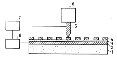
Here, Fig. 3 shows simply an example of the
recording medium preparation method by use of the
lithographic method. First, a thin film of an
15 electroconductive material which becomes the counter-
electrode 2 is formed on the substrate 1 (Fig. 3A).
On the counter-electrode 2 is formed an organic
recording layer 3 having the electrical memory effect
(Fig. 3B), and a thin film of an electroconductive
20 material which becomes the fine lone electrode 4 is
formed thereon over the whole surface (Fig. 3C).
Next, as shown in Fig. 3D, the voltage is applied with
the power source 5 for initialization between the
counter-electrode and the electrode layer to
25 initialize the whole recording layer. Then, by use of
the lithographic technique, fine lone electrodes 4 are
~ - 33 -
2022929
1 formed to desired sizes and shapes (Fig. 3~) to
prepare a recording medium. Fig. 3F is a view of the
recording medium as seen from above.
However, according to the recording
5 preparation method as described above, there has been
employed the method in which an electroconductive
layer for fine lone electrode was formed on the whole
surface of an organic recording layer, then a voltage
is applied to effect initialization and fine lone
10 electrodes are formed by photoetching process, but it
is not necessary to limit the method to this. For
example, after formation of an organic recording
layer, fine lone electrodes may be also formed by use
of the lift-off process. However, in this case, a
15 resist is formed to a desired pattern on the organic
recording layer, and an electroconductive thin film
for fine lone electrodes is laminated thereon over the
whole surface before application of a voltage for
initialization between the counter-electrode and the
20 fine lone electrodes, followed by formation of fine
lone electrodes according to the lift-off process.
The applied voltage for initialization of the
recording has employed in the example of the present
invention a triangular wave of a wave height value of
25 + 10 V and a period of 20 sec. as shown in Fig. 4, but
the wave height value, the period and the waveform are
- 34 -
2022929
1 not limited to these, but any condition which can
perform initialization stably may be employed.
However, concerning the wave height value, + 5 V to +
15 V is preferable in characteristics of the device.
5 This is because no stable initialization can be done
at a value smaller than + 5 V, while if over + 15 V,
deterioration of the device is liable to occur. The
voltage application time, which may also depend on the
wave height value of the applied voltage, may be
10 preferably 180 sec. or shorter in view of
deterioration of the device. Concerning the waveform,
in addition to a triangular wave, a sine wave, a
rectangular wave, etc. may be employed.
Also, as to the electrode shape of the fine
15 lone electrode, a square type, a round type, etc. may
be conceivable, but these are not limitative, but any
desired shape can be chosen. Also, as to the size of
the fine lone electrode, various sizes can be adopted,
but in view of recording density, those as small as
20 possible are preferred. For example, sizes of 10000
~m2 or less, preferably 1 ~m2 or less at which the
density becomes as high as that of the optical memory,
are preferred, and the size of the electrode may be
also made smaller to the extent of the size of the
25 molecule because the recording layer itself can be
utilized as the molecular memory.
~ - 35 -
2022929
1 On the other hand, the materials of the
substrate electrode (counter-electrode) to be used in
the present invention may be one having high
electroconductivity, as exemplified by enumerous
5 materials, including typically metals such as Au, Pt,
Ag, Pb, Al, In, Sn, Pb, W and alloys thereof, further
graphite and silicide, still further electroconductive
oxides such as ITO, and these may be considered to be
applicable to the present invention. As the electrode
10 formation method by use of these materials, the thin
film formation techniques known in the art may be
satisfactory. However, the electrode material to be
formed directly on the substrate should be desirably
an electroconductive material which will not form an
15 insulating oxide on the surface during formation of LB
film, such as a noble metal or an oxide
electroconductive material such as ITO, etc.
As the material for the probe electrode, any
material which exhibits electroconductivity and can
20 apply a voltage on the recording layer through fine
lone electrodes may be available, as exemplified by
Pt, Pt-Ir, W, Au, Ag, etc. The tip end of the probe
electrode is required to be pointed so far as possible
corresponding to the size of the fine lone electrode.
25 In the present invention, the probe electrode is
prepared by controlling the tip end shape of the
- 36 -
2022929
1 needle-like electroconductive material by use of the
electro chemical polishing method, but the preparation
method and the shape of the probe electrode are not
limited to these at all.
When a device with the MIM structure as shown
in Fig. 8 is prepared by use of the materials and the
film forming method as described above, a memory
switching device exhibiting the current-voltage
characteristics (the electrical memory effect) as
10 shown in Fig. 9 and Fig. 10 is obtained, and it has
been already found that the two states ~ON state which
is the low resistance state and OFF state which is the
high resistance state) have respectively the memory
characteristics. The memory characteristic means that
15 the previous state is maintained, so long as the
voltage applied does not exceed a specific value
(threshold value). These memory switching
characteristics are realized for those with layer
thickness of 4 A to some 1000 A, but the recording
20 medium in the present invention should preferably have
a layer thickness in the range from 10 A to 1000 A~
most preferably from 50 A to 500 A. When built-up
films are formed by the LB method to form an organic
insulating film, the number of layers laminated should
25 be preferably about 1 to 50. In the laminated layers,
layer thickness as mentioned above, the resistance
2022q29
1 preferable in memory characteristics is desirably some
M Q or higher in OFF state.
In Fig. 8, 84 represents a substrate, 41 an Au
electrode, 42 an Al electrode and 43 the monomolecular
5 built-up films.
Fig. 2 illustrates schematically the device
for performing recording and reproduction onto the
recording medium of the present invention. In Fig. 2,
5 is a probe electrode for applying a voltage on the
10 recording medium, and by application of a voltage from
the probe electrode through the fine lone electrodes
onto the recording layer, recording and reproduction
are effected. 6 is a movement control mechanism in
the XYZ directions (three-dimensional fine movement
15 control mechanism), and with this, recording and
reproduction can be effected by movement of the
position of the probe electrode to the fine lone
electrode at any desired position. ~ is a pulse power
source, 8 a signal reader, performing recording by
20 application of a voltage on the recording medium from
the pulse source or performing reproduction by
detection of the current which flows through the
recording medium by the signal reader.
Fig. 5 is a block constitutional diagram
25 showing the recording and reproducing device of
another embodiment of the present invention. In Fig.
` -
- 38 -
202292~
1 5, 106 is a probe current amplifier which is also
equipped with a circuit for applying a bias voltage
for reproduction. 107 is a servo circuit for
controlling the fine movement control mechanism 108 by
5 use of a piezoelectric element so as to control the
distance between the both so that a voltage can be
applied through the fine lone electrode 103 from the
probe electrode 102 on the recording layer 101. 109
is a power source equipped with a pulse voltage
10 application circuit for recording/erazing for applying
a pulse voltage for recording and erazing through the
fine lone electrode 103 on the recording layer 101
between the probe electrode 102 and the counter-
electrode 104.
110 is an XY scanning driving circuit for
controlling movement of the probe electrode 102 in the
XY direction (recording layer surface direction).
111 and 112 are rough movement control
mechanisms for approaching previously the distance
20 between the probe electrode 102 and the recording
medium 1 on the substrate 105.
115 is an XY stage for rough movement in the
XY direction.
These respective instruments are all
25 controlled centrally by a microcomputer 113. 114
represents a display instrument.
- 3g -
202292~
1 Fig. 6A shows a schematic illustration of a
fine movement control mechanism 108, a probe electrode
102, and the recording medium. The fine movement
control mechanism 108 has electrodes for applying
5 voltages for fine movement control in the directions
of X, Y and Z, respectively, and, for example, as
shown in Fig. 6B, it can scan in the X direction by
application of voltages at + X and - X.
- 40 -
2022q29
1 Referring now to Examples, the present
invention is described.
~xample 1
An optically polished glass substrate
5 (substrate) was washed with a neutral detergent and
Triclene ~Trichloroethylene), then Cr was deposited as
the subbing layer by vacuum vapor deposition
(resistance heating) method to a thickness of 50 A,
and further Au was vapor deposited by the same method
10 to 400 A, to form a counter-electrode.
Next, a chloroform solution containing
squarilium-bis-6-octylazulene (hereinafter abbreviated
as SOAZ.) dissolved therein at a concentration of 0.2
mg/ml was spread onto the aqueous phase of 20 C to
15 form a monomolecular film on the water surface. After
evaporation of the solvent, the surface pressure of
such monomolecular film was enhanced to 20 mN/m, and
further the above electrode sub~trate was dipped
gently at a speed of 5 mm/min. so as to cross the
20 water surface while maintaining constantly the surface
pressure, and further drawn up, thereby building up a
Y-type monomolecular film of two layers. By repeating
this operation for appropriate times, built-up films
of 8 layers were formed on the above counter-electrode
25 to provide a recording layer 3.
Then, on the recording layer composed of the
202292~
1 SOAZ-LB film, a plurality of Al electrodes with a
thickness of 500 A and a size of 50 ~m square were
formed as the fine lone electrodes 4 by the vacuum
mask vapor deposition (resistance heating) method,
5 thereby preparing a recording medium of the present
invention.
Next, on the recording medium prepared
according to the method as described above, the
experiments of recording, reproduction and erazing
10 were carried out by use of the recording and
reproducing device shown in Fig. 2. However, as the
probe electrode 5, a probe electrode made of
platinum/rhodium prepared according to the electro
chemical polishing method is used, and the probe
15 electrode 5 is controlled in its distance (Z) by a
piezoelectric element so that a voltage can be applied
on the recording medium through the fine lone
electrodes 4 on the recording layer 3. Further, the
movement control mechanism 6 is designed so that the
20 movement control can be done in the interplanar (X,Y)
directions. Hence, by the movement control mechanism
6, recording, reproduction and erazing of the fine
lone electrode at any desired position can be effected
by the probe electrode 5.
The recording medium having the recording
layer 3 with 8 built-up SOAZ layers was set on the
~ - 42 -
2022929
1 recording and reproducing device, and first the
position of the probe 5 was determined by visual
observation and fixed firmly. Next, the position of
the probe electrode 5 was controlled by the movement
5 control mechanism 6 so that a voltage can be applied
between the Au electrode 2 and Al electrodes 4 which
become the fine lone electrodes. By application of a
voltage for reading of 1.5 V from the probe electrode
5 which is a voltage not exceeding the threshold
10 value of voltage which causes the memory effect to
occur between the Al electrode and the Au electrode,
the current value was measured by the signal reader 8.
As the result, OFF state was exhibited under ~A or
less. Next, after application of a triangular wave
15 pulse voltage having a waveform shown in Fig. 7 which
is the voltage of the threshold value Vth_ON which
cau~es ON state to occur or more from the pulse power
source 7, the current was measured by applying again a
voltage of 1.5 V between the electrodes. As the
20 result, a current of about 0.7 mA flowed, indicating
that the state became ON state. That is, ON state was
recorded.
Next, after application of a triangular wave
pulse voltage with a peak voltage of 5 V which is the
25 threshold Vth_OFF changing from ON state to OFF state
or more and a pulse width of 1 ~sec., a voltage of 1.5
~ - 43 -
2022q2~
1 V was again applied, whereby the current value was ~A
or less to confirm returning to OFF state.
Next, when the experiments of recording,
reproducing and erazing as previously described were
5 conducted with movement of the position of the probe
electrode 5 to another fine lone electrode different
from the above electrode by the movement control
mechanism 6, entirely the same results were obtained,
whereby it was confirmed that the recording medium of
10 the present invention was effective.
After ON state and OFF state were prepared
according to the methods as described above,
photoirradiation was effected on the recording medium
of the present invention and reproduction was
15 performed by applying again a voltage of 1.5 V at the
site recorded, whereby a current of sub-mA order
flowed even after photoirradiation at the portion
where ON state was exhibited before photoirradiation,
while only a current of ~A or less flowed at the
20 portion of OFF state without recognition of change in
recorded information by photoirradiation. Thus, light
fastness, namely stability was found to be excellent.
Also, both the states of ON state and OFF state could
be stored for a long term of 3 months.
Separately from the above experiment, 7 kinds
of recording media were prepared with recording layers
- 44 -
2022929
1 of 2, 4, 12, 20, 30, 40 and 60, and also for these
recording media, the same recording and reproducing
experiment as described previously was conducted. The
evaluation results are shown in Table 1.
~valuation was made by overall judgement by
goodness of recordability and erasability after
application of a recording writing pulse and an
erasing voltage, further by comparison of the current
values under recorded state and erased state~ON/OFF
10 ratio), and stability. Particularly good one is
represented by ~ , good one O , and one slightly
lower in evaluation as compared with others ~ .
The thickness per one SOAZ layer was
determined by the small angle X-ray diffraction method
15 to be about 15 A .
~xample 2
The same recording medium as in ~xample 1 was
prepared except for using a polyimide in place of the
SOAZ recording layer used in ~xample 1. Also for this
20 recording medium, the experiments of recording,
reproduction and erasing were conducted in the same
manner as in ~xample 1. The results of recordability,
ON/OFF ratio and erasability were summarized in Table
1. Similarly as SOAZ, when a polyimide was employed
25 for the recording layer, recording and reproduction of
data signals could be done without change in data
~ - 45 -
2022929
1 signals by photoirradiation being recognized, whereby
a recording medium with excellent light fastness could
be provided.
The method forming the polyimide film is as
5 described below.
A dimethylacetamide solution containing a
polyamic acid (molecular weight about 200,000)
dissolved at a concentration of 1 x 10 3 % (g/g) was
spread on the aqueous phase of pure water of a water
10 temperature of 20 C to form a monomolecular film on
the water surface. The surface pressure of the
monomolecular film was enhanced to 25 mN/m, and
further while maintaining constantly the surface
pressure, the above substrate was dipped and drawn up
15 by movement at 5 mm/min. so as to cross the water
surface, to build up Y-type monomolecular films. By
repeating such operations, 7 kinds of built-up films
with 12, 18, 24, 30, 36, 42 and 60 layers were
prepared. Further, these films were heated at 300 C
20 for 10 minutes into polyimides.
The thickness per one polyimide layer was
determined by ellipsometry to be about 4 A.
~ - 46 -
202292~
1 Table 1
Organic Built-up Recorda- ON/OFF ~rasa- Light
compound number bility ratio bility fastness
4 0
SOAZ 8
12
40 0
12 0
18
Polyimide24
36
42 0
20 ~xample 3
Experiments were carried out in the same
manner as in Example 1 except for using t-butyl
derivative of lutetium diphthalocyanine tLUH(Pc)2] in
place of the SOAZ layer used in Example 1. However,
25 the layer numbers of the recording layers were made 8
kinds of 2, 4, 8, 12, 20, 30, 40 and 60 layers
202292~
1 similarly as the SOAZ recording layers.
The results of the recordability, ON/OFF
ratio, erasability and light fastness were entirely
the same as in the case of SOAZ recording film, and
5 similarly as SOAZ, recording and reproduction of data
signals could be done also in t-butyl derivative of
lutetium diphthalocyanine ~LuH(Pc)2], without
recognition of change in data signals by
photoirradiation. Thus, light fastness was found to
10 be excellent.
The built-up conditions of t-butyl derivative
of LuH-(Pc)2 are as follows.
Solvent: chloroform/trimethylbenzene/acetone
(1/1/2~
Concentration: 0.5 mg/ml
Aqueous phase: pure water, water temperature
20 C
Surface pressure: 20 mN/m
Substrate vertical movement speed: 3 mm/min.
Examples 4 - 6
By use of a polyimide as the recording layer,
recording media were prepared by use of the electrode
materials shown in Table 2 and the same experiments as
25 in Example 1 were carried out, whereby the results
shown in Table 2 were obtained. As shown by the mark
~ - 48 - 2022929
1 ~ in the Table, concerning all of the recording
media, sufficient recording and reproducing
characteristics and light fastness were obtained.
The layer number of the polyimide LB films was
5 24 in all the Examples. Au electrode was vacuum
deposited by use of the resistance heating method, Pt
electrode by the EB method and IT0 by the sputtering
method.
10 Table 2
Exam- Counter- Recording Fine lone ~ecording Light
ple electrode layer electrode reproduc- fastness
tion
4 Pt Polyimide Al
IT0 Polyimide Al
6 Pt Polyimide Au
Example ~
A recording medium was prepared in the order
shown in Fig. 3.
First, an optically polished glass substrate
(substrate 1) was washed with a neutral detergent and
Triclene, then Cr was deposited to a thickness of 50 A
25 as the subbing layer by the vacuum deposition
(resistance heating~ method, and further Au was vapor
- 49 - 2 0 2 29 2 9
1 deposited to 400 A by the same method, to form a
counter-electrode.
Next, by use of the LB method, 24 built-up
layers of a polyimide monomolecular film were formed
5 to provide a recording layer 3.
On such polyimide recording layer 3 Al was
formed to 1000 A according to the vacuum vapor
deposition (resistance heating) method. Then, by use
of a power source 5 for initialization as shown in
10 Fig. 3D, and by applying a triangular wave with a wave
height value of + 10 V and a period of 20 sec. as
shown in Fig. 4 as the voltage for initialization of
the recording layer between the Au electrode which is
the counter-electrode and the Al electrode previously
15 formed, initialization of the whole recording layer
was effected.
Next, on the Al electrode was spinner coated a
posi-type resist material (trade name: OMR-83) to a
film thickness of 1.2 ~m, followed by exposure,
20 developing and post baking. Then, Al was etched in
lattice shape to a pattern size of 2 ~m square with 2
~m intervals with a solution of H3P04:HN03:CH3COOH:H20
= 16:1:2:1. Such substrate was subjected to acetone
ultrasonic cleaning, dimethylformamide (DMF)
25 ultrasonic cleaning, pure water washing to peel off
the resist, followed by baking, to form plural fine
~ - 50 -
202292~
1 lone electrodes 4 with sizes of 2 ~m square (see Fig.
3F).
Next, on the recording medium prepared
according to the method as described above, the
5 experiments of recording, reproduction and erasing
were conducted by use of the recording and reproducing
device shown in Fig. 2. However, as the probe
electrode 5, a probe electrode made of
platinum/rhodium prepared by the electro chemical
10 polishing method was employed, and the probe 5 was
controlled in its distance (Z) by a piezoelectric
element so that a voltage could be applied through the
fine lone electrodes 4 on the recording layer 3 onto
the recording medium. Further, the movement control
15 mechanism 6 was designed so as to be controllable also
in the interplanar (X, Y) directions, while having the
above-mentioned function. Hence, by the movement
control mechanism 6, recording, reproduction and
erasing of the fine lone electrode at any desired
20 position can be effected by the probe electrode 5.
The recording medium having a recording layer
3 with 24 built-up layers of polyimide was set on the
recording and reproducing device, and first the
position of the probe 5 was determined by visual
25 observation to be firmly fixed. Next, the position of
the probe electrode 5 was adjusted by the movement
2022929
1 control mechanism 6 so that a voltage could be applied
between the Au electrode and the Al electrode which
becomes the fine lone electrode. When the current
value was measured by the signal reader 8 by applying
5 a voltage for reading of 1.5 V which is a voltage
(bias voltage) not exceeding the threshold value
voltage which causes the electrical memory effect to
occur between the Al electrode and the Au electrode
from the probe electrode 5, a current of sub-~A order
10 flowed to indicate OFF state, whrereby the recording
layer was found to be initialized. Next, after
application of a triangular pulse voltage having a
wave he.ight value of the threshold value voltage Vth
ON which gives rise to ON state or higher from the
15 pulse power source 7, the current was measured by
applying again a voltage of 1.5 V (bias voltage)
between the electrodes, a current of about 0.7 mA
flowed, thus indicating establishment of ON state.
That is, ON state was recorded.
Next, after application of a triangular pulse
voltage with a peak voltage of 5 V and a pulse width
of 1 ~sec which is a voltage of the threshold value of
voltage Vth_OFF or more at which the change from ON
state to OFF state occurs, a voltage of 1.5 V (bias
25 voltage) was applied again, whereby the current value
at this time was found to be sub-~A order and
~ - 52 - 2022929
1 confirmed to be returned to OFF state.
Also, both ON state and OFF state could be
stored for a long term of 3 months.
Next, the experiments of recording,
5 reproduction and erasing as described previously were
conducted with movement of the position of the probe
electrode 5 by the movement control mechanism 6 to a
plurality of fine lone electrodes separate from those
as mentioned above, the recording layer was
10 initialized in every fine lone electrode to give the
same results for all of recording, reproduction and
erasing, whereby the recording medium of the present
invention was confirmed to be effective. That is,
according to the recording medium preparation method,
15 it has been found that the size of 1 bit can be made 2
~m square, whereby a high density recording medium
comparable with an optical memory can be provided.
Also, separately from the above, 6 kinds of
recording media with layers of 12, 18, 30, 36, 42 and
20 60 were prepared, and for these recording media, the
same recording and reproduction experiments as
described previously were conducted. The evaluation
results are shown in Table 3.
~valuation was made by overall judgement by
25 goodness of recordability and erasability after
application of a recording writing pulse and an
2022929
1 erasing voltage, further by comparison of the current
values under recorded state and erased state (ON/OFF
ratio), and stability. Particularly good one is
represented by ~ , good one O , and one ~lightly
5 lower in evaluation as compared with others ~ .
The thickness per one layer of polyimide was
determined by the ellipsometry method to be about 4 A.
Table 3
Organic Built-up Record- ON/OFF Erasa-
compound number ability ratio bility
12
18
24
Polyimide 30
36
42 O
Example 8
According to the same method as in Example 7,
a counter-electrode of Au and recording layers of
polyimide (24 layers) were formed on a glass
25 substrate.
On such polyimide recording layers were
- 54 -
2022929
1 spinner coated a nega-type resist material ~trade
name: RD-2000N-10), followed by pre-baking. The film
thickness at this time was made 0.7 ~m. Subsequently,
exposure, development, post-baking were performed to
5 prepare a resist pattern so that fine lone electrodes
with a size of 2 ~m square could be formed in lattice
shape with intervals of 2 ~m.
On such substrate, Au which becomes the fine
lone electrodes was deposited over the whole surface
10 to 1000 A by the vacuum vapor deposition method.
Then, by application of the same voltage for
initialization as in Example 7 between the counter-
electrode and the Au electrode on the resist,
initialization of the polyimide recording layer was
15 effected.
Next, such substrate was subjected to acetone
ultrasonic cleaning, DMF ultrasonic cleaning, pure
water washing and baking, a plurality of fine lone
electrodes with a size of 2 ~m square were formed by
20 lift-off to prepare a recording medium.
Also, for this recording medium, the same
experiments as in Example 7 were conducted, whereby
every fine lone electrode was found to be initialized,
and also the same results as in Example 7 were
25 obtained for all of recording, reproduction and
erasing.
~ - 55 - 2022929
1 Also, the same recording medium as described
above was prepared with polyimide recording layers of
12, 18, 30, 36, 42 and 60. As the result, entirely
the quite similar results as in Example 7 were
5 obtained, whereby it could be understood that the
recording media were effective.
Examples 9 - 11
By use of the same lift-off as in Example 8 as
the method for forming fine lone electrodes, recording
10 media were prepared by use of the electrode materials
shown in Table 4 and the same experiments as in
Example 8 were conducted to give the results shown in
Table 4. As shown by the mark ~ in the Table,
concerning all the recording media, initialization of
15 the whole surface of the recording portion could be
effected at one time, and yet sufficient recording and
reproduction characteristics could be obtained.
The layers of the polyimide LB film are all 24
layers. Au electrode was formed by the resistance
20 heating method, Pt electrode by the EB method and IT0
by the sputtering method, respectively.
-
~ - 56 -
2022929
1 Table 4
Exam- Counter- Recording Fine lone Initial- Recording,
ple electrode layer electrode ization reproduc-
tion
9Pt Polyimide Al
10IT0 Polyimide Al
11Au Polyimide Pt ~ ~
In the ~xamples as described above, the LB
method was employed for formation of the organic
compound recording layers, but a film forming method
which can prepare a film very thinly can be used
without limitation to the LB method, and as such
15 method, film forming methods such as MBE, CVD methods,etc. may be specifically mentioned.
Also, concerning the formation method of the
counter-electrode and the fine lone electrodes, as
already mentioned, a film forming method which can
20 prepare a uniform film can be used, and the vacuum
vapor deposition method is not limitative.
Further, the substrate materials and shapes
thereof are not limited at all in the present
invention.
As described above, according to the recording
medium of the present invention, the following effects
~ - 57 -
2022929
1 can be obtained.
~ 1) As compared with optical recording, a
recording medium with very excellent environmental
resistance, particularly light fastness could be
5 obtained.
(2) Since the recording layer is formed of
built-up monomolecular films, film thickness control
on the order of molecular size (several A to several
10 A) could be easily realized. AlsOr due to
10 excellent controllability, reproducibility is high in
forming the recording layer.
(3) Since the recording layer may be thin,
productivity is rich and an inexpensive recording
medium can be provided.
(4) Since one information is recorded per one
fine lone electrode, by miniaturization of the
electrode, a recording and reproducing device with
higher density than optical memory device can be
provided in the future.
(5) Since initialization of the whole
recording medium can be done at one time, the time and
labor for initialization could be made minimum.
(6) Since initialization of the recording
medium can be done in the recording medium preparation
25 steps, the device for initialization can be omitted
from the recording reproducing device, whereby the
2022929
1 recording and reproducing device can be made simpler.
(7~ Since recording, reproduction and erasing
can be done by contact of a probe electrode with fine
lone electrodes previously provided, fine control of
5 the distance between the probe and the recording
medium surface becomes unnecessary, whereby
stabilization of recording and reproduction and access
to the recording site become easier.
(8) Since the system of recording information
10 per one fine lone electrode is adopted, by arranging
previously the fine lone electrodes regularly as
desired, it also becomes possible to perform tracking
with the recording bits, namely the fine lone
electrode themselves. By this, no guide groove is
15 required to be formed.