Note: Descriptions are shown in the official language in which they were submitted.
C'~r,~
P~TENT APPLICATION IN C~NADA
Attorney Docket No. 680~Xx
TITLE: "HAND-HELD DATA CAPTURE SYSTEM
WITH INTERCHANGEABLE MO~ULES"
BACXGROUND OF THE INVENTION
This inYention generally relates to data collection
systems whersin a hand-held unit is operated from battery
power and functions to collect and process data by a
seguence of automated and manual operatio~s. ~ typical
automated process is the non-cc,ntact scanning ~f b~r code
data by means-of a cyclically deflected laser beam or with
the use of an image photosensor of the CCD type. Once a
valid bar code reading has been obtained, a keyboard ~ay be
manually operated to indicate an associated ~uantity. The
user may then manually initiate a further operat;on, or
example, the on--line transmission of the data to a remote
host computer e.g. via a radio frequency communications
link.
The presently known data capture d~vices which include
a user interface such as a keyboard and display, and a non-
contact automatic reader function have tended to be highly
specialized, bulky and expensive. Tn a prior art device
having the desired functions, it may be necessary to
completely invert the device after a bar code reading, in
order to view the display, and/or to actllate the keyboard.
Devices which essentially add a keyboard and display
to an existing scanner design may be particularly awkward
to use, for example because the keyboard and display are
applied at the forward end of the scanner where they are
not conveniently accessible and where manual forces applied
to thc keyboard are tedious to counteract with the
supporting handle which is much closer to the user's body.
It would be desirable to have a basic data capture
terminal which is light weight and compact, and which could
be readily con~erted for on-line wireless communications
,
.
- . : :
. ~ -, ,
'
, ~ . , , '
.
--2~ r~
and bar code scanning as needed. Such a versatile data
capture system would be particularly suitable for small
scale operations where low cost i~ a ~aljor objective, and
versatility vf the terminal unit is especially
advantageous. Furthermore, in order to realize the
benefits of mass production, it is clesirable from the
manu~acturer's standpoint if a basic computerized terminal
configuration can be readil~ adapted to the needs of
diverse end users by the selective addition of low cost
~odules.
SUMMARY OF TE~E INVENTI ON
In accordance with an important aspect of the present
invention, a light weight low cost basic terminal can be
adapted for on-line RF communication with a host computer
and selectively accommodate high throughput bar code
scanners of the in~tant type such as CCD bar code scanners
and deflected laser beam scanners, while essentially
avoiding the deficiencies in the prior art devices.
It is highly desirable that the data capture sy~tem be
compatible with existing peripheral equipment e~g. for
downloading data to the terminal and where applicable
recharging the terminal batteries. In a particularly
advantageous embodiment a basic terminal unit has one end
with external contacts compatibIe with existing
communicating and recharging docking apparatus and an
opposite end adapted to selectively receive various modular
adaptor end caps. ~esides a compatibility end cap
providing standard overall dimensions and a standard
electrical connector arrangement compatible with an
existing printer docking receptacle, the terminal may be
coupled with an automatic bar code scanner or other desired
peripheral device. The basic terminal may receive an RF
module adapting the terminal for on-line RF communications.
In accordance with preferred features, the ~F module
can be removed and replaced with another similar module
without requiring any tuning adjustments. Further such
module interchange can most preferably be carried out in
C'~ ~ ;ri ~
--3--
the field by the end user. secause of such capability the
useful life of the basic terminal ma~ be extended without
service interruptions for return to the factory or service
center, and the ter~inal is readily upgraded and adapted to
new operating require~ents. For example different
operating frequencies can be selected simply by replacing
the RF module. This is achieved by stocking only the
desired ~odules which are of low cost in comparison to the
total sy~tem. Si~ilarly, the laser scanni~g ~omponent may
be a6sociated with the basic terminal only as needed, the
basic terminal alone being used where vnly thi~ ty~pe of
capability is required.
An object of the invention is to provide a basic
terminal configuration of compact light weight construction
but which is readil~ adapted to wireless data communication
with other components of a data capture system such as a
host computer, and which preferably retains a capability
for coupling with a non-contact self scanning type bar code
reader or other highly efficient data capt~re co~ponent.
Another object is to provide such a basic terminal
configuration which can be quickly and easily associated
with a wireless transceiver module without requiring
special tools.
A further object of the invention resides in the
provision of a basic terminal configuration with modular
means for providing RF communications capability or the
like. Preferably the RF- module can be replaced in the
field without requiring any tuning adjustment.
Still another object of the invention relates to the
provision of a hand-held type data capture system wherein a
basic low cost light weight terminal unit can selectively
receive various modules such as an RF module, but such
system retaining the option of co~patibility with existing
communicating and /or recharging docking receptacles ~e.g.
o a portable printer or the like~.
In an illustrated embodiment, an RF adaptor module is
electrically coupled with a co~trol microprocessor of the
~ , ,
'.': ', . "' " ' ' ' '' ~
-4-
basic ter~inal configuration. The control microprocessor
~ay be installed on a peripheral circuit carrying member or
control board within the terminal, and the peripheral
control board in turn may have pin and socket type coupling
with a host printed circuit board mounting a main computer
processor. The RF adaptor module may have a standard
external connector fitting and may contain electrical
connector means therefor which automatically engage with
mating electrical connector means on the péripheral control
board as the end cap module is mechanically applied t~ the
terminal. Radio frequency and~or scanner cabling from the
peripheral control board may pass through a slot in the end
wall of the terminal and may be manually connected with the
receive/transmit or scanner circuits and/or external
connector of the RF module prior to fastening of the module
to the terminal, or automatic coupling means may be
provided for the ~F and/or scanner circuits as well as for
the standard external connector fitting.
The mating parts of the terminal are modular in the
sense that they can be readily disconnected from each
other. One modular part can be disconnected, removed as a
unit, and replaced with a part of the same or different
configuration. For example, a wireless communication
module is readily disconnected from the terminal, removed
as a unit, and replaced. Further in preferred form each
~odular part has only ~uick disconnect type signal coupling
with the other parts, and most preferably the parts are
self-guided so that the couplings are achieved as the
automatic result of correct mechanical interfittinq of the
parts, as the parts are pressed together. In the preferred
embodiment, the wireless communication module has definable
performance characteristics which permit it to be tested
and adjusted as a separate unit. Then the various wireless
communication ~odules can be interchanged without requiring
any further tuning or adjustment. In an embodiment within
the scope of the present invention, a terminal may receive
diferent types of modules selectively e.g. a wireless
J ~
communication module or a eombined wireless cnmmunioation
and automatic reader module. In one such terminal, the
basic terminal parts may comprise a use~ interface top
layer and a battery-containing layer underlying
approxi~ately one half of the interf,ace layer. The
communication module or the combined communication and
reader module may be selectively interfitted with the basic
terminal p~rts to form a highly compact light weight
terminal which is particularly comfortably gripped e~ g. in
the vicinity of the battery containing layer.
In existing prior art units, electrostatic discharge
protection is afforded by use of conductive ~etallic
enclosures or by use of metallic sheathing applied to the
inner walls of the enclosure of the devices, such sheathing
or metallic enclosures being electricall~ connected to
ground terminals of external devices when interconnection
of hand held data entry terrninals with such external
devlces is effected. Such m~thods of electrostatic
discharge protection are susceptible to transient signals
coming into the data entry terminals over interconnection
circuitry from the external devices, though affording
reasonable protection from transient signals created by
electrostatic discharge arising on the exterior of the
unit.
A preferred data entry terminal according to the
present invention is provided with a plurality of
electrically conductive pads generally coplanar with the
external surace of the terminal housing and fixed thereto.
Such surface contact pads may be interconnected by internal
circuitry to respective connector elements of a D-type
connector mo~nted upon a housing end cap such that recharge
power and data communication pathwa~s may be made through
either or both of such contact means. The surface contact
pads are positioned such that they ma~ be engaged with
mating elements of an external device, the mating elements
having sufficient resilience to ensure reliable electrical
contact with the conductive pads. This results in a
~' ' ~ , -.
.
6- ~c~7~9
particularly rugged and facile means for interconnectlng
the terminal with peripheral devices.
The preferred data entry terminal is pro~ided with
integrated electrostatic discharge protection associated
with the incoming signal paths of the device. ~ecause of
this, the housing of the data entry terminal may be
constructed of lighter materials and molded from pol~meric
materials into an a~sthetically pleasing and comfortably
held form. The expensive application of métallic sheathing
i~ avoided while isolation of sensitive circuit components
from electrostatic discharge transients is achieved. Th~s
an object of the invention is to provide a hand--held data
entry terminal having advantageous electrostatic discharge
characteristics, even where the terminal has an array of
unshielded surface contact. pads embedded in a terminal
casing of nonconductive material.
The electrostatic discharge ~ESD) protection for the
preferred terminal may be provided exclusively through
transient suppressing circuit techni~ues and board ~ounted
transient suppression devices arranged in such a manner as
to protect the entire electronic circuitry of the terminal
from the potentially harmful effects of transient signal
phenomena, including that introduced to the ter~inal
through any external connectors. The elimination of
shielding devices commonly used to provide protection f rom
transient signal phenomena on previous types of portable
computer terminals may enable lighter, molded pol~meric
materials to be used in the ~anufacturing process of
certain components.
The preferred terminal contains a central processing
means, and control circuitry associated with the processing
means and including signal carrying pathways leading from
the surface contact pads, the circuitry having transient
suppressing circuit elements associated with the signal
carrying pathways.
Other objects, features and advantages will be
appar~nt from the following detailed description, taken in
.
- . ,
:, . , ,: '
~ . .
? rJ~
connection with the accompanying drawings, and rom the
individual features and relationships o the respective
appended claims.
BRI13F DESCRIPTION OP T~lE DRAWINGS
FIG. 1 i~ a somewhat diagrammatic frontal perspective
view sho~ing a hand-held data capture terminal which may be
modified as shown ;n FIGS. 6-10 and FIGS. 11-19, to orm
embodiments of the present invention. ,
FIG. 2 is a somewhat diagrammatic exploded view of the
hand held terminal illustrated in FIG. 1.
FIGS. 3 and 4 are schematic diagrams showing the major
electronic circuits and components contained within the
ter~inal of FIGS. 1 and 2 and the interconnections between
them, FIG. 4 showing preferred circuit details for the
power control components of FIG. 3.
FIG. S is a plan view show;ng the interior of the end
cap of the terminal shown in FIGS. 1-4.
FIG. 6 is a perspective view of an embodiment
incl~ding the basic terminal of FIGS. 1-5 and further
including provision for on-line radio frequency
communications capability.
FIG. 7 is an exploded perspective view of the modular
adaptor end cap of the embodiment of FIG. 6.
FIG. 8 is an exploded perspective view of the
embodiment of FIG. 6.
FIG. 9 is a block schematic diagram showing the
electronic system components o the embodiment of FIG. 6.
FIG. 10 is a block schematic diagram similar to FTG.
9, but showing an i~proved circuit arrangement for
facilitating interchangeability of the RF end cap module
and in particular avoiding the need for any tuning
adjustments when an RF end cap module is applied to the
basic terminal in the field.
FIG. 11 is a somewhat diagrammatic perspective view
showing a modular hand-held data capture device in
accordance with the present invention.
:
' . .
-8~ J
FIG~ 12 is a side ele~ational view showing a RF data
terminal in solid lines, and indicating with dash lines a
scanner module ~hich is mated there~ith~ to form the
unitary hand-held data capture device of FX~. 11.
FIG. 13 is a top plan view of the scanner module which
forms part of the data capture device of FI~. 11.
FIG. 14 is a side ele~ational view of the scanner
modul~ of FIG. 13, showing the handle detached ~ut in
vertical alignment with its attachment,~ position, and
showing locating studs on the handle which fit into the
scanner body during assembly therewith.
FIG. 15 is a bottom plan view of the scanner body,
showing the sealed slots which serve to locate ~ handle
therewith.
FIG. 16 ifi a front end elevation~l view o~ the data
capture device of FIG. 11.
FIG. 17 is a rear end elevational view of the data
capture device of FIG. 11.
FIG. 18 is a somewhat diagrammatic side elevational
view, similar to FIG. 12, but illustrating with dash lines
a modification wherein the scanner module is provided with
contacts at a rear end thereof for engagement with the
external set of contacts of the terminal unit.
FIG. 19 i~ a diagrammatic view indicating an exemplary
lay out of parts within the scanner module of FIGS. 11-17
or FIG. 18.
FIG. 20 is a somewhat diagrammatic exploded view o~
the basic terminal of FIGS. 1-8, but with a memory card
controller board substituted for the peripheral controller
board of FIG. 2.
FIG. 21 is a somewhat diagrammatic exploded view of
the top end vf the terminal of FIG. 20 showing the memory
card electrlcal connector/receptacle, and also showing a
back-up lithium battery with an associated mylar insula~ing
strip which may be present in any of the illustrated
embodiments.
~ ~ . ' . .
~ ' .. ' .
.
~ . ~
-, , . '
Fig. 22 shows exemplary transient suppressing
circuitry which may be associated with the surface contact
pads of the preferred basic ter~inal of FIGS. 1-8 and 11.
DETAILED DESCRIPTION C1F FIGS. 1--10
FIG. 1 shows a portable hand-held data capture
terminal 10 embodying aspects of the present invention.
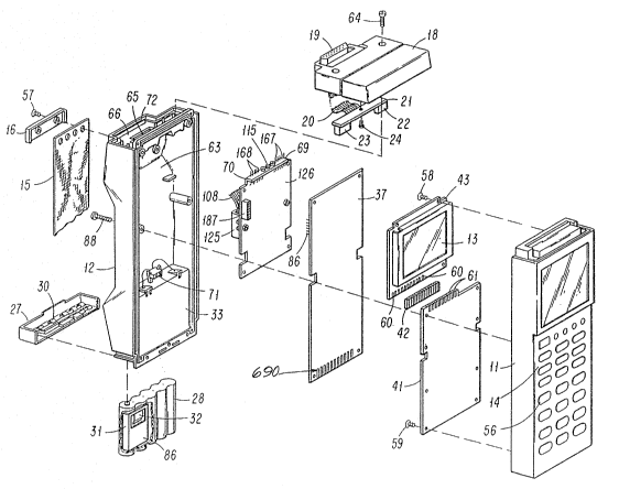
The te~minal 10 has an elonqated housing formed of parts 11
and 12, the back housing part 12 of which is formed in a
manner s~ as to e~able a user to hold the device
comfortably in one hand for extended periods of time.
In the preferred embodiment of the invention, ter~ninal
10 may be powered by a rechargeable nickel~cadmium battery
pack 28 (FIG. 2) or a plurality of ~ size batteries.
Enclosed within the terminal housing 11, lZ are four
permanently mounted printed circuit boards 26, 37, 41, and
43, (FIG. 2), namely a host printed eircuit board 37, a
display printed circuit board 43, a keypad printed circuit
board 41, and a peripheral controller printed circuit board
26. Interconnections betwee~ the circuit boards are
acco~plished through a plurality of pin and socket type
connectors including pin type connectors 86 and mating
receptacle type connectors 87. An exception is the
interconnection between displa~ board 43 and keypad board
41 which is accomplished throuqh a resilient conductive pad
42. When assembled, front housing part 11 and back housing
part 12 are joined together by a plurality of screws 88.
The front housing part 11 of the terminal 10 provides
a mounting platform for a display 13 (FIG. 2) which m~y
provide a visual indication of various types of
information. In the preferred embodiment of the invention,
display 13 is of a liquid crystal display (LC~ variety
: providing sixteen lines, with twent~ characters per line,
of di~play area. Optionally, the display 13 may be of a
four line type. The displa~ 13 may be mounted upon a
display printed circuit board 43 which is then mounted or
secured to front housing part 11 by a plurality of screws
.
' ' '
- 1 0 - F~ J,
58. In addition, the front housing part 11 may provide a
mounting platorm for a keypad 14 (FIG. 1), having a
plurality of ~eys 56 thereon. In the preferred embodiment
of the invention, keypad 14 is provided with either twenty-
three or forty keys. The control and interface circuitry
for keypad }4 may be contained on keypad printed circuit
board 41 (~IG. 2) which is mounted or secured to front
housing part 11 by a plurality of screws 59.
Electrical interconnections betweén the display
printed circuit board 43 and keypad printed circuit board
41 may be accomplished through a resilient, conductive pad
42, which may be located bet~een overlapping portions of
the aforementioned circuit bcards and retained in this
location by means of the pressure exerted upon it when the
respective circuit boards are mounted in the housing part
11. Conductive pad 42 may contain a plurality of generally
parallel, spaced apart conductive elements embedded within
it. The overlapping portions of display printed circuit
board 43 and keypad printed circuit board 41 each contain a
plurality of coplanar, generally parallel, and evenly
~paced apart connector elements 60 and ~1, respectively.
The respective conductive elements of conductive pad 42,
when conductive pad 42 is mounted between the overlapping
portions of keypad printed circuit board 41 and display
printed circuit board 43, are in positive contact with
corresponding aligned connector elements 60 and 61, and
provide respective paths for the transfer of electrical
signals therebetween. Alternatively, the required
electrical interconnections between display printed circuit
board 43 and keypad printed circuit board 41 may he
accomplished through a flexible multi-conductor ribbon type
cahle.
The back housing part 12 of the terminal 10 may
provide a mounting platform for a removable, elastic type
flexible strap 15 (FIG. ~). Flexible strap 15 may allow
the u~er of the terminal 10 to relax the user's grip on the
terminal 10 for short periods of time, without actually
~ t 5
removing the terminal 10 from the user's hand. The
flexible strap 15 may be secured to the bottom of housing
part 12 by means of two ret~ining cla~ps such as 16 (~IG.
2). Retaining cl~mps 16 are secured to housing part 12
through the use of screws such as 57, with two screws 57
securing each retaining clamp. In the preferred embodiment
of the invention, retaining clamps 16 may be re~oved with
simple hand tools, allowing the flexible strap 15 to be
easily replaced. seneath the flexible strap 15 and
generally between retaining clamps 16, the bottom of
housing part 12 is contoured in ~uch a wa~ that, when the
terminal 10 is being held by the user, the user's hand is
placed on a recessed area 62 ~FIG. 1) in housing part 12
and beneath flexible strap 15.
Referring to FIG. 2, the top end of the terminal 10
may be enclosed with a removable end cap 18. End cap 18 is
attached with two screws 64 to housing part 12. When
installed on terminal 10, end cap 18 overlies and encloses
cavity 63. Located on, and p~rt of the end cap 18 may be a
multiple pin D-sub type connector 19, which may in turn be
direct or hard wired via a flexible multi-conductor ribbon
type cable 20 to a connector platform 21, on which may be
mounted two connector receptacles 22 and 23. Cable 20,
connector platform 21 and connector receptacles 22 and 23
may also be mounted on and be part of end cap 18. Screws
such as 24, FIG. 2, may secure parts 21, 22, 23 in a
precise locat.ion with only connectors 22, 23 projecting
beyond the confines of the end cap housing~ The multiple
p;n D-~ub connector 19 may provide a communi~atiQnfi pnrt
capable of the two-way transfer of data with other
compatible de~ices according to the ~S-232C standard as
defined by the Electronic Industries Association. When end
cap 18 is installed on terminal 10, receptacles 22 and ?.3
automatically mate with a plurality of pins 67 and 68 which
protrude through connector blocks 69 and 70. Pins 67 and
6~, and connector blocks 69 and 70 are each attached or
connected to peripheral controller board 26. In a
preferred e~bodiment of the invention, the end cap 18 may
be removable using common hand tools. Alternatively, a
plain type of end cap housing which does not contain a D-
s~b connactor 19 or any of its associated components such
as 20-23, may be used in place of end cap 18. In addition,
peripheral controller board 26 provides the electronic
circuitry required to interface the two-way data transfer
which may occur through D-sub connector 19. In a preferred
embodi~ent, eontroller board 26 may be a peripheral type
device which may be exchanged or otherwise config~ed to
enable the ~se of vari~us types of end cap devices. I~hese
various end cap devices ~ay enable terminal 10 to perform a
wide variety of functions not currently possible with
existing hand held data capture devices including, but ;n
no way limited to, the two-way transfer of data throu~h
space using radio frequenc~ waves as the data carrying
medium, the two-way transfer of data over telephonic
communication links, and the two-w~y transfer of data
between the terminal and a bar code reading device.
Referring again to FIG. 2, the cavity of the housin~
part 12 receiving the battery pack 28 may be enclosed by a
battery compartment hatch 27. The battery compartment
hatch 27 may have attached to its surface a plurality of
conductive metallic type contacts 30. Metallic contacts
30, in conjunction with a plurality of metallic springs
located in the battery compartment, may complete the
electrical path of the batteries enclosed in the battery
compartment. When the battery compartment hatch 27 is
properly installed on the terminal 10 t it comes in contact
with a conductive metallic rod which extends the length of
the battery compartment and is hard wired to battery supply
~onn~ctor 71, ~IG. 2, and compl~t~ th~ ground or negative
potential path for the batteries. The enclosed batteries
are arranged in the battery compartment in a series type
configuration to provide the required voltage. The
positive potential of the battery path is completed by the
hard wiring of a metallic spring to battery supply
'
.
connector 71. ~attery supply connector 71 contains a
plural~ty of receptacles whic~ mate wit:h host board 37 to
provide the battery power to the terminal 10~ sattery
compartment hatch 27 attaches to the bott:o~ housing part 12
of terminal 10 through the interlocking and meshing of
railings on both the battery compartment hatch 27 and
bottom housing part 12. The battery co~part~ent is formed
by a cavity within terminal 10, with a somewhat rectangular
opening on which three corners are rounded and one corner
is somewhat squared.
sattery pack 28 may be constructed of a plurality of
nickel-cadmium batter~ cells, arranged in such a way as to
provide approximately six volts of direct current
electrical power. In addition, battery pack 28 may contain
a formed metallic plate 31 which may be attached to the
nickel-cadmium batteries in such a way as to orm a
somewhat squared edge on one corner 86 of the battery pack
28. The so~ewhat squared corner 86 (FIG. 2) of the battery
pack 28 may correspond with the previously described
somewhat squared corner on the rectangular opening of the
battery compartment, and ma~ prevent the improper insert;on
of battery pack 28 into the battery compartment. In
addition, metallic plate 31 may be further formed to create
a conductive metallic shunt 32 (FIG. 2~. When battery pack
28 is installed in computer terminal 10, metallic shunt 32
engages probes to create an electrically conductive path or
short circuit between the probes. The probes may form part
of the battery charging circuit of the terminal ~0 and may
disable this circuit when not electrically shorted
to~ether, thereby preventing the inadvertent and possibly
hazardous application of recharging electrical power to
non-rechargeable (e.g. alkaline) batteries.
In place of the battery arrangement 28, the batteries
can be mounted in an enclosed drawer part with square and
rounded edges, which slides endwise into a receiving
compartment. External contacts on the drawer may be
substituted for the array of external contacts as shown at
.
- ~ ' '' ~ .
.
322, FIG. 11. The rear e~ternal contacts at the drawer
external wall may be connected with respecti~e spring
contacts at the forward end of the dr~wer which spring
contacts engage with fixed contacts in the roof of the
battery compartment as the drawer is fully inserted.
coin operated latch may be rotatable through a give~
angular amount in one direction to lock the battery drawe~
in place, and may be rotatable in the opposite direction to
unlock the battery drawer.
Descrip~ion of FIG._
Referring now to FIG. 3, the terminal functional block
diagram is illustrated. A cen~ral processor unit (CPU) 74
may cont~in program storage and reside on the host printed
circuit board. CPU 74 controls all terminal functions,
executes machine instructions in proper sequence, and
supervises data communication with devices inside and
outside the terminal 10. However, it may allow an optional
auxiliary processor unit on the peripheral controller board
26 to control some external access (e.g. reading from
and/or writing to an auxiliary memor~ card). The CPU 74
may abort all- communications throughout ter~inal 10 should
power available from the main batteries (e.g. nickel-
cadmium battery pack 28) drop below a predetermined level.
All access to static RAM 75, the real time clock 76, the
keypad 14 and keypad circuit board 41, and display 13 and
display circuit board 43 are accomplished through CPU 74.
The CPU 74 also controls the charging current applied to
battery pack 28 by control of CHGON line 46, FIG. 4, an~
generates a signal on MEMON line 50 to initiate a sleep
mode of the terminal. In addition, CPU 74 allows
activation of the 485 circuit and watchdog timer component
77, RS232 level converter 78, and the backlight of display
13.
The memory in static RAM 75 is decoded in the decode
circuit 7~. MEMDIS line 83 is coupled with this circuit
and will inhibit access to static R~M 75 in the event the
.
..
- ..
.
. . . .
-15- ~3~
five volt regulator 80 has dropped out of regulation,
indicating the installed batteries (e.g. nickel-cadmium
battery pack 28) are no longer providing the neces~ary
voltage. In the preferred e~bodiment of the invention,
memory in tha ~tatic RAM 75 may be selectively configured
in one of varying sizes.
The terminal 10 may be equipped with a battery/charge
monitor circuit 81 as well as a battery charge circuit 82.
The battery/charge monitor circuit 81 m~nitors the main
battery and provides a signal on the ~owsATT line if
battery voltage drops below a certain value. The signal on
the LowsATT line in~orms the CPU 74 that battery power i~
getting low, and CPU ?~ in turn will notify the user
through the display 130 The terminal 10 will continue to
operate normally as long as the Lows~TT line rem~ins in a
high logical state. If the LOW~TT line goes low, the
terminal 10 will switch to its inactive (sleep) state, but
will be allowed to become active if a key 56 (FIG. 1) is
pressed. ~ further output of the monitor component 81 is
the DDEC line. The DDEC line pro~ides a true indication if
the five volt regulator 80 begins to drop out of
regulation. When the DDEC line goes low, the terminal 10
switches to sleep ~ode promptly, saving all dat~ in the
~tatic RAM 75, which will have backup power in the event
that the main batteries are re~oved. ~inally, when the
output of the main batteries (through five volt regulator
80) drops to a predefined level, the MEMDIS line 83 will
carry a low logical signal, causing the static RAM 75 to be
disablecl, the CPIJ 74 to be reset and the transi~or ~
~FIG. 4),located in the power isolation circuit 84, to
switch to nonconducting mode. The CPU 74 is equipped with
an analog input port which allows it to monitor several
other battery/charge conditions. The signals available at
this port may provide information regarding the charge
level, for example. Another signal which may be monitored
here is an extended duration signal emanating from the
KEYINT line 85. The controller board 26 may also provide
~16-
an inter~upt signal on P~RINT line 86, which is made
available to the CPU 74 on this analog port.
The charge circuit 82 is disabled unless a sho~ting
mechanism (conductive metallic plate 32, FIGS. 2 and 4)
which is located on and part of the nickel-cadmium battery
pack 28, is present and properly installed in the battery
co~partment as described previously. Charging of an
installed nickel-cadmium battery pack 28 occurs
automatically when a charge voltage of !a predeter~ined
value is present on CHARGE line 87. Charging of the
installed nickel-cadmium battery pack 2a may occur
selectively at a rate of approximately twenty milliamps or
a rate of approximately seventy-five ~illiamps, and is
determined by the ter~inal software through CPU 74. The
CPV 74 also mon~tors the a~bient air temperature and, if
below a predeter~ined level, preferably approximately five
degrees Celsius, the CPU 74 causes the LOWTEMP line 88 to
provide a signal, which causes constant current charge to
default to the lvwer charge (twenty milliamps) rate. When
terminal 10 is first attached or otherwise connected to a
charger, the C~GDET line 89 goes active for approximately
four milliseconds, then returns to its inactive state. Thi~
causes NMI generator 90 to generate a pulse to wake the
terminal lO from its sleep mode and signal that a charger
is present.
A charger must be attached to terminal 10 far the 485
circuit and watchdog component 77 to function, as this
circuit is powered by the charger. The 485 circuit and
watchdog circuitry 77 may provide the terminal 10 with a
communications port capable of synchronous two-way data
co~unication with other compatible devices, transferring
data at a rate not greater than five hundred thousand bits
per second, according to the predominate RS485 standard as
defined by the Electronic Industries Association. When CPU
74 detects the presence of a charger, it activates the 485
circuit and watchdos through ~50N line 91. Data may then
be transmitted and received by terminal 10 on RS485 DATA-
~
.' ~' , .
.
,
- ' ' '
-17-
line 92 and RS485 DATA-line 93, these lines being connected
to a pair of a number of coplanar, gene:rally parallel and
evenly spaced conductive metallic pad~s 322 (FIG. 11~.
Received data is applied to the CPU 74 from the 485 circuit
and ~atchdog circuit 77 on 485RXD line 9~, while
transmitted data is applied to the 485 ciccuit and watchdog
circuit 77, from CPU 74, on 485TXD line 96.
Five volt regulator 80 may operate from either the
main battery supply or an attached charger. If both are
present, the output voltage of the charger will e higher
than the battery voltage, causilng five volt regulator 80 to
choo~e current from the charger supply rather than the
batteries. This is accomplished through "O~" wiring of
diodes 97 and 98.
Ter~inal 10 has been designed to be in an inactive
state ~sleep mode) for the majority of time to conserve
battery power. As described previousl~, NMI line 55 must
be pulsed for terminal 10 to wake up and begin program
execution. The pulse on NMI line 55 is generated by the
NMI generator 90 and may be generated by a pulse on ~EYINT
line from the keypad 14, a pulse on RTCINT line from the
real time clock 76, simultaneous pulses on LOWsATT line and
DDEC line, a pulse on C~GDET line 89, a pulse on PERINT
line 86 from peripheral controller board 26, or a pulse on
the PWRUP line ~from the 5v regulator 80).
Power is applied to the peripheral controller board 26
under the control of CPU 74. Once the controller board
power is stable and the contro].ler board microprocessor
(212, FIGS. 9 and 10) is stable, the controller board
microproces~or begins a hand shaking sequence with CPU 74
to establish a communication link. This link has some
~oftware support to monitor data integrity throughout the
transfer of data~ The co~troller board 26 is equipped with
a pair of analog switches which isolate the data bus on the
contrvller board 26 from the memory data bus on the host
printed circuit board 37. This i.solation prevents
inadvertent data bus interference dur.ing the power up
routine of the peripheral controller board microprocessor.
, .
- ~ :
-18- ~ s 7 ~
Description of FIG. 4
Referring to FIG. 4, unique battery charging and
terminal sleep mode circuits are illustrated. When
terminal 10 is attached or otherwise connected to a
compatible recharging device, a charging ~oltage may be
introduced on the C~RGX line ~FIG. 4~. The charging
voltage on C~RGX line 43 may then be applied to a voltage
regulating deYice 44 e.g. type LP 2951 ACM. The regulated
charging volta~e output of regulating device 44 may be
applied to a transi~tor switch 45 through a resistor R73.
Transistor switch 45 may be soft~are controlled, and ~a~ be
activated or turned on when the signal on CHGON line 46
changes its logical state, which may cause field effect
transistor 47 to change state which then ma~ cause
transistor switch 45 to change state. Transistor switch 45
may provide a constant charging current through a diode
CR3, to the installed battery pack 2~, for a predetermlned
length of time. The charging current may be applied to
installed battery pack 28 through metallic terminals in the
battery compartment shorted by ~etallic shunt 32 on the
battery pack, FIG. 2.
The sleep mode circuitry of terminal 10 monitors the
input aotivity of the terminal 10 and, when no activity is
detected for a predetermined length of time, may cause the
terminal 10 to shift to a stand-by or sleep mode to
conserve the power supplied by the installed batteries.
When in the inactive state, the memory array and real time
clock circuits of terminal 10 require less power than when
in an active state. In operation, when the ter~ina] 1n h~s
been inactive (e.g. no keys 56 are pressed on ke~pad 14)
for a predetermined amount of time, MEMON line 50 ~ay
pulse. This pulse may be sensed on the CLR input of flip-
flop integrated circuit 51, which may cause its Q output to
switch levels. Resistor R140 and capacitor C96 may ensure
that no false signals are received by flip-flop 51. ~he Q
output of flip-flop 51 is designated MEMS~ line 52. The
state of MEMSW line 52 may cause field effect transistor 53
--1 9 Ç'D ~ b,~
to change state. MEMSW line 52 may be ~iltered by resistor
R88 and capacitor C93. When field effect transistor S~
changes states, it greatly reduces thle amount of current
flowing through the base of transistor 54 by causing
resistor R59 to be placed in series with resistor R60. The
greatly reduced current flow through the b~se of transistor
54 allows the regulated supply of the terminal 10, provided
by the power of the installed batteries applied through a
voltase regulating device, to provide l~ss current, thus
increasing the active life of the installed batteries.
When term~nal 10 again becomes active (e.g. a key 56
is depressed on keypad 14) N'MI line 55 may pulse. The
pulse on NMI line 55 may be sensed by flip-flop 51, FIG. 4,
at its CLR input, and may then cause the Q output of flip-
flop 51 to change state. The state of MEMSW line 52, FIG.
4, at the Q output of flip-flop 51 may now cause field
effect transistor 53 to reset to its former state,
returning current flow through the base of transistor 54 to
its active level.
The ter~inal 10 may operate exclusively from the power
supplied through a regulating device by the installed
batteries (e.g. battery pack 28, FIG. 2~ until the MEMDIS
line 83, FIG. 4~ changes state. The MEMDIS line ~ay change
state when the installed batteries or attached charger do
not provide suficient voltage to operate the terminal.
When the MEMDIS line changes state, it may change the state
of field effect transistor Q15. The MEMDIS line may be
filtered by resistor R141 and capacitor, C94. When field
effect transistor Q15 changes state it may cause
interruption of current flow through the base of transistor
54, effectively removing the regulated supply of terminal
10 from the ~emory array. When this occurs, a standby
lithium battery or a charged capacitor may supply the
memory array and real time clock circuits until such time
that the main power supply is returned to the level
required to power the terminal 10~ ~ charged capacitor may
provide short term back up power for the terminal 10, with
,, . . ., . . . . ............................................. :
,
,: : . .
. . . ' . ~ , .
-20- ~ ;~,'J;`fll
the lithium battery providing power when the stored charge
of the capacitor is depleted. The lithium battery may
provide long term back-up power. When the mai~ power of
terminal 10 is restored to an operational level, the MEMDIS
line 83, FIG. 4, may return to its form~er state which may
restore normal current flow through the base of t{ansist~r
54.
Pescription of FIG. 5
FIG. 5 is a view looking into the interior o~ end cap
18. Three screws such as 24 secure the connector pla~form
21 at the correct position within the end cap 18. Two
guide parts 38 and 39 are precisely located so as to
project into the open end 72 of housing part 11 and
interfit with cooperating surface~ at the end 72 so as to
in~ure that the connector receptacles 22, 23 are correctly
aligned with pins 67, 68 as the end cap 18 is applied to
the terminal. This type of mechanical guidance could also
be provided for the automatic electrical interconnection of
all of the various modules herein which are t~ be
mechanically joined with each other.
Description ~f FIGS. 6 thrvugh 10
Referring to FIGS. 6-10, an embodiment of the
invention is disclosed for providing wire]ess data
communication with a remote receiver. In FIG. 6, it can be
seen that terminal 110 includes the basic housing parts 11
and 12 of FIGS. 1-5, and is further provided with a modular
adaptor end cap 118. Antenna 104 and external connector
fitting 119 are attached to the end cap 11~
(Corresponding reference numerals have been applied to
identical parts in FIGS. 1-5 and 6-10 and such parts need
not ~e further described). ~eys 56 are depressed by the
user to enter data and to control the functions of terminal
110, including causing terminal 110 to transmit or recei~e
data by radio transmission means. Display 13 provides
visual information concerning RF transmissions received by
the terminal.
.
,
: , . . .
: ~ .
--2 1-- ,~ J Q ~
From FIG. 8, it can be understood that end cap 118 may
be readily removabl~ mounted on housing parts 11 and 12.
External connector fitting 119 provides for interconnection
to optional peripheral devices and is electrically
connected through wiring 120 to connectors 122 and 123
which are mounted to connector platfor~ 121. Connectors
122 and 123 engage ~ith the pins of mating connectors 67
and 68 (FIG. 2) of peripheral controller card 26 when end
cap 118 applied to housing parts 11 and 12..
Radio module 106 mounts within end cap 118 by suitable
mountin~ means such as indicted b~ screw 107 (FIG. 8), and
is electrically coupled to peripheral controller card 26 by
ribbon cable lOB. Ribbon cable 108 is detachably connected
to radio module 106 by a connector 109 affixed to the end
of c~ble 108, and enters housin~ part 11 through opening 65
in wall 66. Ribbon cable 108 connects at 25, FIG. 2, with
the peripheral controller card 26, and serves to inter-
connect radio module 106 and peripheral controller card 26.
Adjusting elements 114 (FIG. 8) are provided on radio
module 106 for frequency tuning and signal level adjustment
purposes.
Referring now to FIG. 7, it can be seen that end cap
118 comprises housing members 116 and 117 which may be
separated when end cap 118 is removed from housing parts 11
and 12 in order to provide access to adjusting elements 114
o~ radio module 106.
Referring to the block diagram of FIG. 9, it can be
appreciated that radio module 106 houses transmitter 202
which is coupled to antenna 104. Transmitter 202 ;.
coupled to transmit level adjust circuitry 204~ Receiver
206 is coupled to antenna 104 and to receive level adjust
circuitry 208. Dashed line A separates the components
located on radio module 105 from components located on
peripheral controller card 26. Control microprocessor 212
communicates with main microprocessor 74, FIG. 3 r of
housing part 11 through coupling means 214 which is
provided by connectors 86, 87, FIG. 2. Control
' ' ` ' : ':
. ' ',.
-22~
microprocessor 212 is coupled to transmitter 202 and
receiver 206 by coupling means 216 along which are
communicated radio control signals. Data to be tran~mitted
is received from processing unit 74, FIG. 3, and is
forwarded by eontrol microprocessor 212 over TX data line
218 to modulation generator and limiter component 220.
Modulation generator and limiter component 220 is coupled
to first low pass filter 222. Data received by antenna 104
is delivered to control microprocessor 212,on RX data line
223 which couples control microprocessor 212 to data
recovery element 224 which is coupled to a second low pass
filter 226~ Lines 108a and 108b and also lines 216 are
part of ribbon cable 108 and serve to couple the circuitry
of peripheral controller card 26 to radio module 106.
External connector fitting 119 is coupled to control
microprocessor 212 by scanning interface signal lines 22
associated with connectors 67, 68, FI~. 2, and 122, 123,
FIG. 8, and wiring 120, FIG. 8.
Peripheral control adjustment elements 115 are mounted
to peripheral controller card 26 such that these adjustment
elements 115 are accessible to the user through opening 65,
thereby obviating the necessity of any disassembly of
housing parts 11 and 12 in order to effectuate adjustments
to the peripheral controller card 26.
In operation, the user may remove mvdular adaptor end
cap 118 from housing parts 11 and 12 when adjustment of
radio components is desired. ~djusting elements 114 ~FI~.
8~ may be accessed by the separation of housing members 116
and 117 (FIG. 7) while radio module 106 continues to be
electrioally connected with peripheral controller
components on card 26 through ribbon cable 108. In
addition, peripheral control adjustment elements 115 (FIG~
8) of peripheral controller card 26 (FIG. 2) may be
accessed when end cap 118 is removed from housing parts 11
and 12. The user may communicate with a remote host
computer in i'real time" by operation of keyboard 14 which
provides signals to main microprocessor 74 (FI~. 9). Main
.
' ~
~,
-23- fA~v ~
microprocessor 74 processes the signals and communicates
them to control microprocessor 212 of peripheral controller
card 26. Control microprocessor 212 iand its associated
circuitry on peripheral controller card 26 processes the
signals to sllperimpose them upon radio transmission
frequencies, and communicates the processed signals to
transmitter 202 which is coupled to antenna 104 and which
thereby causes their transmission through space from
antenna 104 by electromagnetic radiation, A remote host
computer responding to terminal 110 transmits radio
frequency signals which are received by receiver 206
through antenna 104. Received signals are processed on
peripheral controller card 26 ~nd are provided to control
microprocessor 212 which communicates the processed signals
to main microprocessor 74. Microprocessor 74 displa~s the
received information upon display 13 so that it can be
observed by the user.
FIG. 10 shows a modification of the embodiment of FIG~
9 which enables the replacement of the RF adaptor module
without requiring a tuning ad~ustment of the module. In
this embodiment the control microprocessor 212 is on the
peripheral controller card, while components 220, 222, 22A
and 226 are included in the radio module 106-1 forming part
of the RF modular adaptor end cap ll~-1. This results in a
digital interface at 250 between the peripheral controller
card of the basic terminal and the radio module of the RF
adaptor end cap.
Since the signals transmitted across the digital
interface are at standardized logic levels, there is no
need for tuning ad}ustment of the RF module to adapt it to
a particular basic terminal. The lines 216, 218 and 223
~ay form part of a ribbon cable corresponding to cable 108
with a connector corresponding to connector 109 for plug-in
coupling with a mating connector of radio module 106-1
Multiconductor line 228 ma~ be implemented via mating
connectors such as 67, 22 and 68, 23 (FIG~2) as in the
previous embodiments~ In e~ch embodiment, power from the
.. . . .
., . . ' , :
.
. . : , -, .
:' - . . . .
.
-24-
battery pack 28 may be supplied to the circuitry of th~ RF
end cap under the control of a ra~io on/off switch 252, the
power supply path 254l FIG. 10, being comprised by
conductors of a ribbon cable such as 108, for example The
control microprocessor 212 is coupled with switch component
~52 as indicated at 2S6, so that all power to the RF end
cap can be s~itched on and off as required to minimize
battery drain.
.Since the peripheral circuit means including 212, FIG
10, only transmits standardized digital signals and battery
power to the Modular adaptor end cap, the end cap circuits
can be pre-adjusted at the factory and adjustments by the
end user in assembling the modular adaptor end cap with the
terminal can be avoided. The peripheral circuit board 26
(FIG. 2) and end cap 18 can be replaced by peripheral
controller board 126, FIG. lO, and the end cap 118-1 with
radio module 106-1, without re~uiring any other hardware
changes in the terminal. Then the end cap with radio
module 106~1 can be replaced with a new identical end cap
as needed without re~uiring any adjustments in the di~ital
outputs from the peripheral controller board, and without
requiring any tuning adjustments of the modular adaptor end
cap.
To replace the modular adaptor end cap 118-1 with the
RF module 106-1, the end cap is removed as in FIG. 8, and
the RF section 106-1 separated at connector 109, ~IG. 8.
new end cap is then coupled with ribbon cable 108 by means
of connector corresponding to 109. This completes the new
digital signal paths which are as represented at 216, 218,
223, 254, FIG. 10.
Exam le Accordin~ To FIG. 10
P
In an exemplar~ embodiment according to FIG. 10, the
basic hand-held terminal configuration formed from housing
parts 11 and 12, FIG. 2, has peripheral adaptor circuit
means 126, FIG. 10, connected therewith via peripheral
connector means similar to 108, 109 (FIG. 8), accessible at
. ' ~ ' ,' ,
-25-
the upper end of the terminal configuration (see FIG. 8).
The basic ter~inal selectively receives a compatibility end
cap (e.g. 18, FIG. 2~ for enclosing the upper ~nd and
providing a resultant hand-held terminal of dimensions
compatible with an e~isting terminal recept~cle e.g. of a
portable printer. In the portable printer the receptacle
for the terminal has an electrical connector at one end for
mating with connector 19, FIG. 1, and a spring-urged
retainer at an opposite end for retaining the termina:L in
operative relation to the printer receptacle.
Where it is anticipated that the terminal
configuration is to be later adapted to provide an RF link
to an external transceiver, the basic terminal
configuration may be provided with peripheral adapter
circuit means such as represented at 126, FIG. 10. The
peripheral input/output means at digital interface 250,
FIG. 10, may be embodied in a cable and connector (such as
108, 109, FIG. 8) which is pas~ively contained within a
compatibility end cap module such as 18, FIG. 1, but is
ready for plug-in connection with ~F module 106-1, FIG. 10,
of a modular adaptor end cap 118-1, FIG. lO.
DESCRIPTION OF FIGS. 11 T~TROUGH 19
In the illustrated embodiment of FIGS 11-19, a unitary
hand-held data capture device 310 comprises housing parts
11 and 12 forming a data terminal body 311, a RF module 312
(corresponding to module ll~, PIG. 9, or 118-1~ FIG lO), a
scanner module body 313 and a handle 31~. The data
terminal formed by components 311 and 312 has a frnntal
face 316 with user-device input and/or output interface
means such as a manual data entry keyboard 14 and a display
means at 13. The frontal face may have an indentation
pattern at 320 for assisting in the aiming of the device in
relation to a data souFCe such as a bar code label on a
product container or the like.
In ~ preferred construction, the terminal body 311 has
a set of e~ternal contacts 322 for coupling of power and
-26~
data signals of various types. The RF module 312 may
~nclude a stub antenna 104 projecting in a longitudinal
direction, and the scanner bod~ 313 may include a scanner
extension part 326 which serves to direct scanner energy
(e.g. optical energy) obliquely to the general plane of the
frontal operating panel 316A This serves to insure that
under normal scanning conditions, the frontal panel 316
will be facing the user during scanning operation so that
for example, the user can verify the scanner data as it
appears on the display 13.
FIG. 12 shows the device 3:10 as having a rubber bumper
331, 332 extending about the exterior sides of the teFrninal
bQdy 311 and the RF module 312 to protect the device 310
against lateral impact.
A connector 334 corresponding to connector 119, FIG.
8, e.g. a standard 15-pin D subminiature connector, may
face longitudinally in a forward direction fro~ a section
335 of the RF module 312. The connector 334 may correspond
in its pin assignments with the connector commonly present
on RF terminals such as the model 2210 RF terminal of
Norand Corporation, Cedar Rapids, Iowa. The connector has
pins assigned to the transmission of scanner signals, RS-
232 signals, charge potential, and power out, for example.
In the illustrated embodiment, the terminal body 311 may
contain rechargeable batteries in a battery compartment at
section 337, and batter~ power may be supplied from the
batteries to the RF module by a direct connection and via
connector 334 to the scanner module.
As shown in FIG. 13, the scanner module body 313 ;s
provided with a connector 340 which is mated with terminal
connector 334 during the assembly of the terminal parts 311
and 312 with the scanner module. A forward recess 343 of
the scanner module body 313 receives terminal housing
sections 335, 33~, while a rearward recess 344 accommodate.s
a transverse rib 345, FIG. 12, on the terminal body 311.
The scanne{ module may have six align~ent ~oles 351-356,
and four screw holes 357-360 or use in securing the
terminal body 311 therewith.
-27~ 3
FIG. 14 shows locating lug~ 361, 362 on the handle 314
which i~terfit with sealed slots 371-374, FIG~ 15, at the
undersurface 375 of the scanner module 313. Four contacts
380 on the handle 314 mate with respective cooperating
contacts 381-384 at undersurace 375, so that for example
the handle 314 may optionally contain batteries and supply
battery power to scanner module 313. The handle is secured
to the terminal by means of an integral internally threaded
nut 38S at the undersurface 375 which likewise is sealed
off from the interior of the scanner module. Thus elements
371-374 and 385 all present blind holes, so that handle 314
may be omitted without the introduction of any exposed
apertures leading to the interior of the scanner module.
As a ~odification, batteries may be removed rom the
terminal body 311, and all operating power for the scanner
and for the terminal keyboard and display and for the RF
components may be supplied from batteries in the handle
31~.
A slide-off battery cap 386 provides access to the
battery compartment within handle 314.
The handle may have a trigger 390 for initiating a
scan operation, and two of contacts 380 may serve as part
of the scan trigger circuit.
As a modification which may be taken to be illustrated
in FIGS. 14 and 15~ the terminal batteries may supply all
operating power to the RF module 3l2 and to the scanner
module 313, and in this case handle 31~ may be omitted to
provide a more compact unitary hand-held data capture
device.
When handle 314 is omitted, scan trigger actuators may
be located at each side of the RF module 312 as indicated
at 391, 3g2, FIG. 16. With this palm supported
arrangement, the device may be held in either the right or
left hand, and the convenient one of the trigger buttons
391, 392 actuated.
FIG. 15 shows a soft rubber guard 401 surrounding a
sca~ner window 402 which may for example serve as an exit
., , ' :
--28-- 3 ~ ? ~ ?~
window for scan energy (e.g. light energy) and as an
entrance window for return scan energy (e.g. modulated
reflected light produced by an incide~t deflected ligh~
beam, or a simultaneous reflected light image where the
incident light substantiall~ simultaneously covers the
entire data source line or lines such as a complete bar
code sy~bol representing complete product information or
the like).
In FIG. 18, center lines 410 and 411 indicate the axes
of elements 351-353, 357, 358 and 354-356, 359, 360, FIG.
13, and center line 412 sho~s the axis of the handle
attachment screw which engages nut 3~5, FIG. 15, to secure
the handle 314 in place.
In FIG. 18, the scanner module may omit connector 340
or leave it unconnected electrically. Instead, th~ scanner
module body is provided with an upstanding end part
420having a set of spring fingers 421 which engage with the
respective external contacts 322, FIG. 11, on the adjoining
end of the terminal. Again the connections may suppl~
terminal battery power to the scanner module, or handle
battery power to the terminal, as well as transmitting the
same scanner signals between the scanner ~odule and the
terminal as in present types of cable connections between
RF terminals and scanners.
As a further alternative scanner power may be supplied
by batteries located in a compartment in section ~25 of the
scanner module.
With batteries in the handle, the center of gravity of
the data capture device 310' of FIG. 1~ and of data capture
device 310 of FIGS. 11-17 may be substantially as indicated
at 427, FIG. 18.
sy way o example, FIG. 19 illustrates a layout of
parts for the case of a scanner module which illuminates a
bar code label or other data source simultaneously over its
entire extent, the reflected light image being stored in an
image sensor array such as a CCD image sensor array for
electronic conversion into a scanner data signal. For
' `, .' ' '
,'. '
-29~ "~
example, respective elements of the reflected light image
may control the generation of charge in respective senso~
elements, the charge states being simultaneously
transferred to a shift register for readout as a serial
scanner data signal.
A scanner o the reflected light image - image senso~
type is shown in U.S. Patent 4,877,949 issued oct. 31,
1989.
The followinq tabulation identifies various components
shown in FIG. 19 and indicates parenthetically the related
reference numerals from the first and third figures of the
incorporated U.S. Patent 4,877,949:
Illuminator 440 (15, first figure; 35, third figure)
Illumination Voltage Generator 441 ~17, first figure)
Automatic Reading Distance Adaptation Means 442 (20,
first figure; 103, 105, 102, 101, 90, third figure)
Image sensor means 443 (ll, first figure) with
photosensor 444 (13, first and third figures)
Control and Processing Means 445 (10, first figure)
FI~. 19 departs from the showing in the third figure
of the referenced U.S. patent 4,877,949 in having the
reflected image follow a single tier longitudinal p~th 450
in the relatively thin layer-like scanner module body 313.
In thi~ way, the thickness of the scanner module body 313
may be substantially less than the thickness of the RF data
terminal, for example. The reflected image path is altered
by a first mirror 451 and a second mirror 452 so that the
image path 450 has a single tier path segment 450A within
extension 326 and a single tier path segment 450s within
the main section of the scanner module.
To further indicate an exemplary layout of parts, a
flex cable 460 may extend from a main circuit board 461 to
the illu~ination voltage gen~rator 441. ~ sensor driver
circuits component 463 may be located adjacent photosensor
443. Control and processing means ~5 may comprise sensor
control circuits 465, signal detection and shaping circuits
466 and control, communication, and decoding circuits 467.
: - . . .
; :
: . . . . .
., . , ,, . - . . , ,, ,: , ' . , . ', ',: ': .
Component 467 may include host I/O buffer means and host
connection means (components 121 and 122 of th~ first
figure of U.S. Patent 4,877,949). Label guide indicator
means (21, first figure), and intensity sensing means (14,
first figure) are indicated at 471, 472 irl FIG. l9.
As represented in FIG. 19, and as disclosed in the
referenced U.S. Patent 4,877,949, a bar code label or other
data ~ource ~ay be read while it is clear of contact with
guard means 401 and e~g. at a variable distance therefrom.
This is al~o true with cyclically deflected laser ~eam
~canning systems which may also be contained in scanner
modules of the essential configuration of scanner module
313.
In place of the flash tube of the U.S. Patent
4,877,949, a series of bright LED light sources collld be
used. Illuminator 440, FIG. 19, may comprise one or more
flash tubes or one or more series of LED sources.
Where the extension 326 is omitted, or where the
exten~ion 326 extends axially of beam path 450~, the mirror
451 i6 of course o~itted. With use of fiber optics or the
like in extension 326, the extension 326 co~ld be
adjustable e.g. fro~ the orientation shown in FIB~ 19 to an
in-line orientation aligned with path 950B. ~ flexible
extension 326 could be manually adjusted to any desired
position over a range of positions e.g. from the in-line
position twith path 450A in alignment with path 450B) to a
sharply angled position (e.g. with path 450A forming an
angle of one hundred and fifty degrees relative to path
450B).
The Preferred RF Data Terminal-Scanner Configuration of
FIGS. 10-19
The RF data terminal 311, 312 as shown in FIGS. 10, 11
and 12 generally may provide the features disclosed in U.S.
Patent 4,910,794 issued March 20, 1990 and European
Puhlished Patent Application EP/0353759/A2 dated February
7, I990. The terminal will run application programs
, ............................... .
.
'"~J '~ ? 7 ~ .
-31-
downloaded to it, or permanently stored in it, or
combinations of both.
When the radio module 312, FIG. 1l, i~ added to the
terminal 311, com~unication is expanded from direct-wired
telecommunication hookups to include real time on-line
communication with a host (e.g. a shared data base,
applications, etc.). Where the peripheral control card
126, FIG. 10, is used for terminal 311, the radio module
itself in the preferred embodiment contains not only the
transmitter, receiver, associated level adjusts and the
scanner connector 334 direct wired back to the control
microprocessor of terminal 311, but also the components
220, 222, 224 and 226 as illustrated in FIG. 10.
The scanner module 313 is treated as an add-on
peripheral to terminal 311, governed by the control
microprocessor 212, as indicated in FIG. 10.
The handle 314 may cortain additional batteries for
extended operation, and to lower the center of gravity o
the device 310 or 310'. ~n option would be to remove the
batteries of the terminal to further lower the center of
gravity of the device 310 or 310'.
The intensity sensing means 471, 472 (see incorporated
U.S. Patent 4/877,949) may be used with a series of bright
kED sources as illuminator, driven full on until a near
saturation of the photosensor is detected, whereupon the
LED sources could be turned off, so that they are treated
as a single shot light source.
A flex Qr rigid interface connection may extend
between terminal 311 and RF module 312 above the level of
sections 335 and 338.
The antenna 104 is offset laterally from connector 33~
(FIG. 12~ to avoid scanner/antenna electromagnetic
interference issues, and may be formed with a right angle
bend as at 324, FIG. 16. The length of antenna 104-1
beyond bend 324 may be adjusted to various desired angulae
positions besides the horizontal disposition shown in FIG.
16. For example antenna element lOA-1 may be disposed
vertically (as the data terminal is viewed in FIG. 16l.
. .
: . ' , ' ' . , ' . : . '' ,
32 ~ $
The terminal control microproces~,or 212, FIG. 10,
controls the supply of battery power to the ~F module as
represented at 118-1, FIG. 10.
The signal levels transmitted at the interface between
the low pass ilters 222, 226 of the terminal peripheral
board 26, FIG. 9, and the transmit and receive level
adjusts 204, 208 of the RF module 10~, e.g. if used for RF
module 312, FIG. 11, may be standardiæed to allow terminals
and modules to be assembled independently, and then mated
in final production, and interchanged in the field, without
re-tuning in either case.
The base-band processing circuitry could be located in
the RF module as in FXG. 10, and in this case digital
~ignals would be transmitted at the interface 250 ~etween
the terminal and the scanner module.
Exemplary scanner technologies which may be used in
the scanner modules of the present disclosure include that
of U.S. Patent 4,882,47S issued November 21, 1989 and that
of U.S. Patent 4,~77,949 issued October 31, 1989. The
di~closures of U.S. Patent~ 4,877,949 and 4,882,476 are
readily applicable to the reading of multiple line bar code
indicia. For example, a two dimensional bar code of
multiple lines can be envisioned occupying an area of 12.25
square centimeters, e.g. a square with sides of 3.5
centimeters. In accordance with an advantageous
de~elopment of one of the inventors named herein, marker
beams may delineate a field of view of square or circular
configuration (e.g. by means of marker beams e~tending at
four corners of a square cross section field o-view). The
multiline bar code or other area information can be at an~
random angular orientation within the field of view as
delineated by the marker beams, and an area image of the
field of view of proper resolution is recorded in a dlgital
image memory, whereupon the digital image may be rotated to
a normalized orientation for decoding, for example. While
a circular flash tube configuration would be of particular
advantage, it is also feasible to utilize linear flash
~ ~ 7~ &~
tubes or series of pulse light sources arranged above and
below a reader window of suitable configuration, e.g. a
rectangular window capable of reading a single line bar
code of a length such as five centimeters directly at the
reading window, and because of the divergence of the
marginal lines (and marker beams) defining the field of
view, also capable of reading a single line bar code at any
random angle providing the bar code is at a suitable
dlstance from the reader window. The same area reader
apparatus would then register a substantial number of line
s~g~ents of a single bar code as a digital image made up of
multiple image lines, or would provide the resolution in
orthogonal directions so as to read a multiple line stacked
or high density area type bar code pattern of any desired
density. A particular advantage of the concepts of modular
automatic reader units and modular automatic wireless
communication units resides in the abilit~ to adapt these
units readily to ever more advanced technological
developments, and to adapt the data terminal embod~ing such
modules to a wide diversity of users or applications. For
example, modules adapted to different size hands and to
left-handed and right-handed users are conceivable~ Also
various user handicaps could be accommodated.
DETAILED DESCRIPTION OF E'IGS. 20 -- 21
As shown in FI~. 20, a memory card 524 may insertable
into a peripheral device connector 525 o a memory card
controller board 526 which replaces peripheral board 126,
FIG. 2. The memory card ma~ be used to increase the
embedded memory of a basic terminal formed of housing parts
11, 12, e.g. by up to five hundred-twelve kilobytes of data
8torage capacity and/or may also store various application
programs which may be run on the terminal. In a preferred
embodiment memory card 524 may contain up to four megabytes
of available memory or progr~mming and still be compatible
with a basic computer terminal such as shown in FIGS. 1
through 8. The memory card may bc easily i~stalled in or
;
. ~
,
5~ ~ s~ '? ~ ;r~,
removed from ter~inal by removal of end cap 18. with end
cap 18 removed, memory card 24 may be inserted in or
removed from peripheral device connector 525 which is shown
in ~ore detail in PIG. 21 as being mounted on and
electrically connected to the memory card controller board
526. When memory card 524 is installed in the peripheral
device connector 525, it occupies an area of cavity 63 and
extends through the opening 65 in wall 66 50 as to be
manually accessible when the end cap 18 has been removed.
~ emory card controller board 526 may contain the
electronic co~ponents and circuitry necessary to control
the operation of memory card 524 as well as to interface
the operation of me~ory card 524 with that of the terminal.
In addition, memory card controller board 526 provides the
electronic circuitr~ required to interface the two-way data
transfer which may occur through D-sub connector 19. In a
preferred embodiment, memory card controller board 52fi may
be a peripheral type device which may be exchanged or
otherwise configured with other peripheral device
controller boards such as 126, FIG. 2, to enable the use of
various types of end cap devices. These various end cap
devices may enable terminal to perform a wide variety of
functions not currently possible with existing hand held
data capture devices including, but in no way limited to,
the two-way transfer of data through space using radio
frequency waves as the data carrying medium, the two-way
transfer of data over telephonic communication links, and
the two-way transfer of data between the terminal and a bar
code reading device.
Other parts shown in FIG. 20 have already been
described with reference to FIG. 2 and have been given
corresponding reference numerals.
Referring to FIG. 21, a lithium t~pe battery 536 may
be mounted upon the host printed circuit board 37 and
retained in position by a non-conductive type of moun~ing
pod 572. When installed, battery 536 ma~ provide stand-by
electrical power to ensure any data stored in the memor~
-35-
circuits is retained should the primary power supply drop
below a predetermined level, and may further maintain the
operation and memory of an integrated circuit type of real-
time clock during the same conditions. The lithium battery
536 may be provided with a electrically non-conductive
(e.g. mylar) strip 538, which when installed between the
battery 536 and an electrically conductive battery
retaining clip 539, may prevent activation of the stand-by
battery power during the aforementioned,conditions until
such a time as the non-conductive strip 538 is removed by
the user. For ease of removal, non-conductive strip 538
may protrude through an opening 40, which may be located on
the top end of computer terminal 10 and under the end cap
18 which may be attached thereto so as to be manually
accessible when the end cap has bcen removed.
Electrostatic discharge (ESD) protection ma~ be
provided exclusively through circuit techniques and board
mounted devices ~rranged in such a manner as to protect the
entire electronic circuitry of terminal 10 from the
potentially harmful effects of transient signal phenomena,
including that introduced to the terminal through any
external connectors such as shown at 322, FIG. 11. The
elimination of shielding devices commonly used to provide
protection from said transient ~ignal phenomena on previous
types of portable data capture terminals may enable
lighter, molded polymeric materials to be used in the
manufacturing process of certain components.
Further Discussion of FIGS. 3 and 4
It will be apparent to those skilled in the art that the
diagrams of FI~S. 3 and 4 are for the purpose of illustration
of selected circuit features, Certain simplifications have
been made. For example, standard parts such as data bus and
address bus components are omitted to avoid cluttering the
.
..
`
.
-36-
drawings with too many lines; further, e.g. in an actual
circuit according to FIG. 4, pin 4 of the regulator 44 is
actually connected to ground through a parallel circuit
comprised of two zener diodes type TMPZ5240 each of a ten volt
value. Thus circuit point 585 is connected with the cathodes
of the two zener diodes, and the anodes of the twc zener
diodes are connected to ground. The shunt cbnductor indicated
at 32 in FIG. 4 may be taken as representing the shunt
conductor 32 of FIG. 20. The below listed components were
given the indicated circuit values in an implementati~n of
FIG. 4:
~53 17.4 ohms .125 watt 1%
R64 61.9 ohms .125 watt 1%
~61 475 ohms .125 watt 1%
R58 one megohm .125 watt 1%
Transistors 45 and 47 were implemented as follows:
Transistor 45 type M~BT 3 9 0 6
Transistor 47 type ZVN 3306
Descri~tion of FIG. 22
-
FIG. 20 shows host printed circuit board 37 with twelve
conductive pads generally designated 690 in FIGS. 2 and 20, and
specifically designated J1-1 through J1-12 in FIGS. 22. The
surface contacts 32~, FIG. 11, may be formed as a free leg of a
U-shaped part. The U-shaped part embraces a grooved edge of end
wall 311~, FIG. 11, e.g. with a tongue part tending to retain the
U-shaped part engaged with the end wall 311~. A free end part
e~tending from the other leq of the U-shaped part includes a
deflectable contact part for pressure engagement with a
respective pad 690 of pri~ted circuit board 37.
~ header is indicated at 86, FIG. 20, on the host printed
circuit board 37, for ~onnecting with a receptacle 5~7 on the
peripheral device circuit board 526. One of such headers may be
associated with lines 701-706, FIG. 22, and the header positions
may bear the desiqnations as follows:
Associated Header Position
Line, FIG. 22 _ Designation
701 DTR
7Q2 DS~
703 TXD
704 RTS
705 CTS .
706 RXD
It is found that a D t~pe connector such as 19, FIG. 20, does
not require the same electrostatic discharge protection as the
surface contacts 322, FIG. 11, since when a potential source
exceeding about 4000 volts is brought into proximity to the
connector 19, an arc is produced to the grounded conductive shell
of the D connector~ even with a probe disposed at the center of
the connector.
Surge protector component 710, FIG. 22, is located closely
adjacent contact pads 690, and is electrically connected with pads
J1-4 through J1-9 as illustrated in FIG. 22, the individual surge
protection eleme~ts being designated SPl-1 through SP1-6 in FIG.
22. The interposed series resistors are designated 22-R4, 22-R6,
22-R8, 22-R15, 22-R16 and 22-R17, and each may have a value of one
kilohm, .125 watt, 1%.
The exemplary electrostatic discharge protection for external
surface contacts 322, FIG. 11, as shown in FIG. 22 provides
protection to level converter 78, FIG. 3, (e.g. type MAX 236~ up
to 20,000 volts~ for example at the following listed ports.
.
.
,
,, . : .
- : .
~ 3 8 ~ r~ ~
Port of Communications
Signal Co~ponent Ty~e MAX 236
Line, FIG. 22 Designation ~~ De~gn~
-
701 DTR 24 T~ OUT
702 DSR 16 R3IN
703 TXD 2 T1 OUT
704 RTS 3 T2 OUT
705 CTS 23 R2 IN
706 RXD 4 Rl IN
Reference numerals 701-706 have correspondingly been applied to
the lines connected with these ports of component 78 in FIG. 3.
The CH~G input from contact J1-12 is connected with C~RGX
line 43, FIGS. 4 and 22, via a conductor 717 having a shunt
zener diode 22-T~l, type sMsG2o~o~ twenty volts. ~n inductance
22-L1, 270 microhenries, could be introduced in series between
conductors 717 and 43 by severing the shunt conductor 718.
The circuitry associated with pads J1-10 and J1-3, and
lines 720 and 721 (designated 485+ and 485~) may comprise a
differential bus transceiver type 75176B: sufficient
electrostatic discharge protection is prov;.ded b~ series
resistance and shunt capacitance networks connected in lines 720
and 721.
In FIG. 11 only dielectric material of end wall 311~, is in
the vicinity of the surface con-tacts 322 at the exterior of the
terminals. Thus there is no external conductive shield in the
vicinity of the surface contacts comparable to the metal shiel~
of the ~-connector 19, FIG. 1. The external surfaces of the
housings are free of such grounded shields over distances about
each surface conductor which are lar~e in comparison to the
spacing between such surface conductors.
It will be apparent that many modi.fications and variations
, ,: ~ -,', , : .
.
-,
: . . , :
-39-
may be effected without departinq f~om the scope of the novel
teachings and concepts of the p~esent disclosure.
.
' ', ' ' :