Note: Descriptions are shown in the official language in which they were submitted.
2~23~9~
The present invention relates to a television
receiver and, more particularly, to a multi-screen
high-definition television receiver for inserting
current television signals in a high-definition screen
and displaying a high-definition image and an image
produced from the current television signals.
Digital integrated circuits have recently
progressed in performance and, in particular, a memory
whose access speed is high and manufacturing cost is
low has been developed. The use of the memory enables
digital processing of video signals. A television
receiver having an image memory for carrying out func-
tions of displaying still pictures and intermittently
and slowly displaying pictures and a PIP ~picture in
picture) function of simultaneously displaying images
on two screens, is commercialized.
The television market needs a high-definition
television receiver having a large-sized screen. An
EDTV (Extended Definition Television) for digitally
processing television signals between frames or fields
and converting interlaced scanning signals into sequen-
tial scanning signals, is developed to display current
television signals with higher quality. The EDTV is
disclosed in IEEE TRANSACTIONS O~ COMMUNICATIONS, VOL.
COM-32, NO.8, AUGUST 198~, "Extended Definition TV Fully
Compatible with Existing Standards" by Fikinuki et al.
On the other hand, a new type high-definition
2023~9~
-- 2 --
television receiver is going to be put into practice.
A high-definition television signal has 1125
scanning lines, interlace scanning of 2:1, a field
frequency of 60.00 Hz, and an aspect ratio of 16:9.
The high-definition television signal enables a wider
screen and twice or more times as high definition in
the longitudinal and lateral directions of the screen
as the current television signal does. The current
television signal has 525 scanning lines and whose
interlace scanning is 2:1, field frequency is 59.94 Hz,
and aspect ratio is 4:3. It is thus possible to enjoy
TV programs with the real ambience. As the high-
definition television receiver, a MUSE ~Multiple
Sub-Nyquist Sampling Encoding) system is used which is
disclosed in INTERNA~IONAL BROADCASTING SYMPOSIUM ON
RADIO AND TELEVISION ENGINEERING, 1985, SESSION 2-(7),
"Transmission of HDTV by MUSE system" by Yuichi NINOMIYA
et al.
When high-definition television receivers are
commercialized in the near future under the condition
mentioned above, the functions of the current television
receivers, especially the PIP function will be certainly
required in the high-definition television receivers.
It is accordingly an object of the present
invention to provide a multi-screen high-definition
television receiver for inserting current television
signals in a high-definition screen and displaying
2 0 2 .~
-- 3 --
a high-definition image and an image produced from the
current television signals.
To attain the above object, there is provided
a multi-screen high-definition television receiver
comprising: first means for receiving and demodulating
a first interlaced scanning television signal; second
means for receiving and demodulating a second interlaced
scanning television signal whose scanning lines are
about twice as many as that of the first interlaced
scanning television signal; sequential scanning conver-
sion means for converting the first interlaced scanning
television signal output from said first means into a
sequential scanning television signal; memory means for
synchronizing the sequential scanning television signal
output from said sequential scanning conversion means
with a field :Erequency of the second interlaced scanning
television signal, time-compressing the sequential
scanning television signal and, converting the sequen-
tial scanning television signal into a third interlaced
scanning television signal in accordance with even and
odd fields of the second interlaced scanning television
signal; and means for selectively producing a fourth
interlaced scanning television signal output from
said memory means and the second interlaced scanning
television signal. According to the above-described
multi-screen high~definition television receiver of the
present invention, sequential scanning signals into
2~23~
which current television signals are converted are
supplied to memory sections, and the sequential
scanning signals are read out from the memory sections
as interlaced scanning signals in accordance with even
and odd fields on the large screen. It is thus possible
to insert a small screen represented by the current
television signal which degrades no image quality, in
the large screen represented by the high-definition
television signal.
This invention can be more fully understood from
the following detailed description when taken in con-
junction with the accompanying drawings, in which:
Fig. 1 is a block diagram showing a multi-screen
high-definition television receiver according to an
embodiment of the present invention;
Fig. 2 is a view illustrative of a state of
multi-screen display;
Fig. 3 is a block diagram showing a sequential
scanning converter of the multi-screen high-definition
television receiver shown in Fig. 1
Fig. 4 is a block diagram specifically showing
a memory circuit of the multi-screen high-definition
television receiver shown in Fig. l;
Fig. 5 is a timing chart showing the operation
timing of the memory circuit shown in Fig. 4;
Fig. 6 is a block diagram showing another example
of the memory circuit shown in Fig. 4;
2023~
-- 5
Fig. 7 is a circuit diagram specifically showlng a
passing detector of the memory circuit shown in Fig. 6;
and
Fig. 8 is a timing chart showing the operations of
the memory circuit shown in Fig. 6 and the passing
detector shown in Fig. 7.
An embodiment of the present invention will be
described with reference to the accompanying drawings.
Fig. 1 is a block diagram showing a multi-screen
high-definition television receiver according to an
embodiment of the present invention.
Fig. 2 is a view illustrative of a current
television screen (small screen) which is inserted into
a high-definition television screen (large screen). In
Fig. 2, reference numeral 201 denotes an area of the
large screen and 202 indicates an area of the small
screen. Since a high-definition television signal and
a current television signal originally differ in the
number of scanning lines, the difference is effectively
utilized in the present invention. The current televi-
sion signal is used as a signal for the small screen
without reducing the number of the scanning lines and,
in other words, without degrading any vertical defini-
tion.
In the large and small screens illustrated in
Fig. 2, the ratio of the length of the small screen to
that of the large screen is 525 to 1125, and thus the
2023~9~
-- 6
width of the small screen is 35 percent (= 525/1125 x
3/4 x loo) of that of the large screen. Accordingly,
the area of the small screen is about 16 percent
(= 525/1125 x 525/1125 x 3/4 x 100) of that of the
large screen.
The arrangement of the multi-screen high-definition
television receiver shown in Fig. 1 will be described.
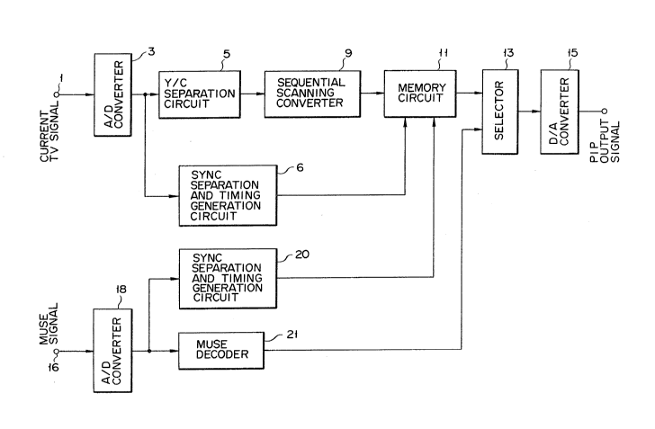
A current-type composite video signal is supplied to
input terminal 1 and then sent to analog-to-digital
(hereinafter referred to as A/D) converter 3. In A/D
converter 3, a current television signal is digitalized
by the clock frequency ~hereinafter referred to as 4fsc)
which is four times as high as the frequency of a color
subcarrier, and the digitalized signal is input to
luminance signal/chrominance signal circuit (hereinafter
referred to as Y/C separation circuit) 5 and sync signal
separation/timing signal generation circuit ~. In Y/C
separation circuit 5, a luminance signal and a chromi-
nance signal are separated from each other and the
chrominance signal is color-demodulated. The separated
luminance signal and chrominance signal are input to
sequential scanning converter 9. In Fig. 1, only a
luminance signal line is shown.
An interlaced scanning signal is converted into a
sequential scanning signal, and then the sequential
scanning signal is input to memory circuit 11.
Memory circuit 11 is designed to adapt the
2023~
-- 7
sequential scanning signal (conversion signal) to a
television signal of a MUSE system. Memory circuit 11
time-compresses the conversion signal to be output as a
signal for the small screen formed by the conversion
signal so that the small screen can be included in
area 202 shown in Fig. 2.
The signal for the small screen is supplied to
one of input terminals of selector 13. The other input
terminal is supplied with a high-definition television
signal from MUSE decoder 21 as a signal for the large
screen. Selector 13 selects the signal for the large
screen during the large screen display period and
selects the signal for the small screen during the small
screen display period. The large screen display period
and the small screen display period correspond to areas
201 and 202 shown in Fig. 2, respectively. An output
signal of selector 13 is supplied to D/A converter 15,
and converted into an analog television signal and
output as a PIP signal.
Memory circuit 11 is supplied with signals of
horizontal sync pulse H and vertical sync pulse V from
sync signal separation/timing signal generation circuit
6 and signals of horizontal sync pulse, filed pulse and
frame pulse from sync signal separation/timing signal
generation circuit 20. Sync signal separation/timing
signal generation circuit 20 separates a sync signal
from a digital MUSE signal output from A/D converter 18
2~23~9~
and generates timing signals of various types. A/D
converter 18 converts a baseband MUSE signal input to
terminal 16 into a digital signal. The digital MUSE
signal output from A/D converter 18 is also supplied to
MUSE decoder 21. The MUSE decoder is described in the
foregoing INTERNATIONAL BROADCASTING SYMPOSIUM ON RADIO
AND TELEVISION ENGINEERING.
Fig. 3 shows the arrangement for processing bright-
ness signals in sequential scanning converter circuit 9
which is a motion adjustable type.
An interlaced scanning signal supplied to terminal
301 is input to field memory 302. An output signal of
field memory 302 is supplied to field memory 303. The
interlaced scanning signal is also input to lH delay
circuit 304, adder 305, speed change circuit 309 and
motion detector 306. lH delay circuit 304 has an amount
of delay corresponding to one horizontal period. Motion
detector 306 carries out an operation corresponding to a
difference in frame between an output signal of field
memory 303 and an input signal of terminal 301 to pro-
duce a motion detection signal. The motion detection
signal is supplied to a control terminal of mixture
circuit 307, and mixture circuit 307 controls the
mixture ratio of two signals input thereto.
Adder 305 adds an input signal and an output signal
of lH delay circuit 304 to produce an average signal.
The average signal is supplied to one of input terminals
2~23~
g
of mixture circuit 307. The other input terminal of
mixture circuit 307 is supplied with an output of field
memory 302 which is a signal before one field. The two
input signals are mixed in mixture circuit 307 in the
ratio according to the motion detectisn signal, and an
output signal (interpolation signal) of the mixture
circuit is input to speed change circuit 308.
Speed change circuits 308 and 309 include memories.
In the memories, the read frequency (clock frequency
8fsc) is twice as high as the write frequency (clock
frequency 4fsc). The period of lH of the current-type
video signal is half compressed. Output signals of
speed change circuits 308 and 309 are supplied to
selector 312. Selector 312 selects the output signals
of speed change circuits 308 and 309 at a half cycle of
lH of the current-type video signal. Thus sequential
scanning video signals (525/1:1) can be produced from
output terminal 313.
Fig. 4 shows the arrangement for processing
brightness signals in memory circuit 11. A sequential
scanning signal input to terminal 401 is sub;ected to
a sampling processing, i.e., a low-band filtering
processing in sub-sampling circuit 402. The number of
samples of lH is reduced from 910 to 455 and therefore
the clock frequency of a signal output from sub-sampling
circuit 402 is reduced from 8fsc to 4fsc.
The conversion signal is input to frame
20~3!~
- 10 --
synchronizing memory 404 capable of asynchronously per-
forming writing and reading operations. Memory 404 is
controlled by memory controller 410. Memory controller
410 is supplied with a small-screen type timing signal
from terminal 414 and supplied with a high-definition
type timing signal from clock generation circuit 416.
Terminal 414 is supplied with a timing signal from sync
signal separation/timing signal generation circuit 6.
Clock generation circuit 416 is supplied with a timing
signal from terminal 415. Terminal 415 is supplied with
a timing signal from sync signal separation/timing
signal generation circuit 20.
A write control signal supplied to memory 404
contains a clock signal (4fsc) and a field reset signal
(59.94 Hz), and a read control signal contains a clock
signal (4fsc = 455 x 525 x 60Hz) and a field reset
signal (60.00 Hz).
A signal output from frame synchronizing memory 404
is thus synchronized with the frame frequency of a high-
definition television signal.
The output signal of memory 404 is supplied totime-compressing memory 406 at the next stage of memory
404. Memory 406 also enables writing and reading to be
asynchronously performed. Although a signal input to
~5 memory 406 is synchronized with the frame frequency of
the high-definition television signal representing the
large screen, it is a sequential scanning signal of 525
2~23~
11 -
scanning lines. In memory 406, time is compressed to
form the small screen as shown in Fig. 2. More specifi-
cally, one of even and odd lines is written in memory
406 by the clock frequency of 4fsc (since an input or
output signal of memory 406 is synchronized with the
frame frequency of the high-definition television
signal, it is known beforehand whether the field of the
large screen is odd or even directly before and after
the signal is input or output), only the available
period of the small screen is read out from the memory
by the clock frequency (44.55 MHz = 1320 sample/H x
1125 x 30) of the high-definition television signal.
This clock frequency will be described later.
Since the number of lH samples of the small screen
is 445, the horizontal period of the small screen with
respect to the large screen is 455/1320 = 0.345 and it
is virtually equal to horizontal period 0.35 shown in
Fig. 2, which hardly causes any problem of distortion of
images with respect to roundness. Memory controller ~13
receives a timing signal generated by clock generation
circuit 416 and a high-definition type timing signal and
supplies write and read control signals.
The signal of Fig. 5(A) is a field reset signal
(59.94 Hz) representing write timing of memory circuit
11 and the signal of Fig. 5(B) is a field reset signal
(60.00 Hz) representing read timing of memory circuit
11. Since memory 404 allows writing and reading
2a~3~
- 12 -
operations to be asynchronously performed, sequential
signals can easily be synchronized with the frame fre-
quency of the high-definition television signal (even
field E and odd field 0) indicative of the large screen.
The signal read out from frame synchronizing memory 404
is input to memory 406. Memory 406 also allows writing
and reading operations to be asynchronously performed.
While the field frequency of the sigr.al output from
memory 404 is converted into 60.00 Hz, the signal has
525 scanning lines and it is a sequential scanning
signal of 1:1. In the odd field period of the high-
definition television signal, only the signal indicative
of an odd line of the signal read out from memory 404 is
written in memory 406. The clock frequency of the writ-
ten signal is the same as that of the signal read out
from memory 404. In the even field period of the high-
definition signal, only the signal indicative of an even
line of the signal read out from memory 404 is written
in memory 406.
The signal stored in memory 406 is read out by
the clock frequency t44.55 MHz) of the high-definition
television signal.
While sequential scanning signals are stored in
memory 404, signals of odd lines or even lines are
selected from the signals read out from memory 404 and
are stored in memory 406. A half of the capacity of
memory 404 is will be sufficient for the capacity of
2023~
- 13 -
memory 406. Fig. 5(C) represents a field reset signal
of memory 406, and Fig. 5(D) shows read timing of memory
406. In Fig. 5(D), a signal for a screen is read out
during the time period represented by oblique lines.
The present invention is not llmited to the above
embodiment.
Fig. 6 illustrates another embodiment of memory
circuit 11. A sequential scanning signal input to
terminal 601 is supplied to field memories 602, 603 and
604 each having a capacity of 1 Mbit (= 455 x 525/2 x
8 bit). A current television type timing signal is
supplied to terminal 606 and a high-definition televi-
sion type timing signal is supplied to terminal 607, and
these signals are input to passing detector 605 and
memory controller 613. Passing detector 605 compares a
field pulse of the current television type timing signal
and that of the high-definition television type timing
signal to detect a field in which the high-definition
television signal representing the large screen passes
the current television signal representing the small
screen and then to supply a passing detection signal to
memory controller 613.
Further, passing detector 605 outputs a discrimina-
tion signal for discriminating between odd and even
fields of the high-definition television signal and
supplies the discrimination signal to memory controller
613.
2~2~
- 14 -
Memory controller 613 outputs a control signal for
controlling the write and read timing of field memories
602, 603 and 604 using the field pulses of the current
television type timing signal and the high-definition
television type timing signal, the passing detection
signal, and the discrimination signal.
Fig. 7 is a block diagram showing passing detector
605, and Fig. 8 is a timing chart showing waveforms of
operation timing of passing detector circuit 605.
In Fig. 7, a high-definition television type
frame pulse is supplied to terminal 701 and then sent
to even/odd field pulse generator 702. A field iden-
tification signal output from circuit 702 is represented
in Fig. 8(A). The identification signal is supplied to
data input terminals of flip-flop circuits 706, 707 and
708, as illustrated in Fig. 7.
on the other hand, a current television type field
pulse is input to frequency divider 704 through terminal
703 and its frequency is divided into halves. An output
of the divided frequency, as shown in Fig. 8(B), is
supplied to flip-flop circuit 707 as a clock signal, and
it is inverted in inverter 709 and supplied to flip-flop
circuit 706 as a ciock signal.
The outputs of flip-flop circuits 706 and 707,
which are shown in Figs. 8(D) and 8(C), are input to
exclusive NOR circuit 714. The output of exclusive NOR
circuit 714 is thus represented in Fig. 8~E). More
2Q23~
- 15 -
specifically, when the high-definition television signal
passes the current television signal, circuit 714 out-
puts a pulse which corresponds to the aforementioned
field detection signal.
Flip-flop circuit 708 receives a frame pulse as a
clock signal and supplies to terminal 716 an even/odd
field discrimination signal, shown in Fig. 8(F), for
discriminating the field of a sequential scanning
signal.
Memory controller 613 is supplied with the current
television type field pulse, high-definition television
type frame pulse, passing detection signal, and even/odd
field discrimination signal.
Memory controller 613 outputs a control signal for
controlling the write and read timing of field memories
602, 603 and 604. Field memories 602, 603 and 604
are controlled the writing and reading operations so
that the cycles of the writing and reading operations do
not overlap each other. Since the field frequency of
the high-definition television signal is 60.00 Hz and
that of the current television signal is 59.94 Hz, the
former signal always passes the latter signal.
When the high-definition television signal passes
the current television signal, if a signal is read out
two times from the field of the current television
signal, the frames of the high-definition television
signal and the current television signal are
2Q23~
- 16 -
synchronized with each other.
Usually, even or odd lines of input sequential
scanning lines are written in field memories 602, 603
and 604. In a passing field period, however, the even
and odd lines are separately written in two of the three
field memories and all the sequential signals are there-
fore written therein. Whether the next field of the
high-definition television signal is an odd field or an
even field, signals of both the odd and even fields are
prepared as signals for the small screen.
The memory circuit shown in Fig. 6 will be further
described with reference to Fig. 8. Fig. 8(G) shows a
pulse for informing the start of picture-in-picture
(PIP). This pulse causes memory controller 613 to
output signals shown in Figs. 8(H), 8(I) and 8(J) and
representing write fields corresponding to memories 602,
603 and 604. As shown in Fig. 8, the writing to the
three memories is performed (wl to w5) in a field period
other than the passing field period. The lines (odd and
even lines) written in the field memories depend on the
even/odd field discrimination signal (Fig. 8(F)) output
from passing detector 605. In Fig. 8 (F), when the
even/odd field discrimination signal represents an odd
field, an odd line is written in the memory and, when
the signal represents an ~ven field, an even line is
written.
When a detection signal indicative of the passing
2~23~
field is produced, as illustrated in Fig. 8(E), the
even/odd field discrimination signal is inverted and
written (w6) in memory 604 (Fig. 8 (J)). Further,
memory 602 (Fig. 8 (H)), which originally writes the
signals in the next field, is so controlled as to
perform the writing operation (w7) in the same frame
as that of writing operation (w6).
In the field next to (w6) and (w7), memory 603
(Fig~ 8 (I)), which originally performs the writing
operation in the next field, performs the writing
operation (w8) in accordance with the even/odd field
discrimination signal. In the further next field,
memory 604 writes a signal in accordance with the
even/odd field discrimination signal (w9). These three
field memories thus perform their writing operations in
the preceding fields. From the field next to tne field
of writing operation (w9), the field memories repeat
normal operations (w10 to w12).
On the other hand, the reading cperations of three
field memories 602, 603 and 604 are carried out at the
same clock rate (44. 55 MHZ) as that of the above embodi-
ment in synchronism with the high-definition television
signal during the available period of the small screen
(Fig. 8 (k)).
Comparing (H) to (J) with (K~ in Fig. 8, it turns
out that the writing time hardly overlaps the reading
time and the signals are processed in the memories.
2Q23~
- 18 -
The signals output from the memories in this manner
form two screens in which a current-type television
image is inserted into a high-definition television
image.
As described above, the current television signals
are converted into sequential signal by motion adaptive
sequential scanning line conversion and read out in
accordance with the even and odd fields stored in the
memories. It is thus possible to insert a small screen
image, whose vertical definition is not degraded at all
with respect to the current television signal, into the
high-definition television image.
As has been described, the present invention
allows a current television screen to be inserted into
a high-definition television screen.
In the above embodiments, A/D converter 3, Y/C
separation circuit 5, sequential scanning convertor 9
and sync separation circuit 6 are used exclusively to
generate signals representative of the small screen.
However, the arrangement of these circuits is an
arrangement of an EDTV circuit which is essential to
a system for receiving MUSE signals which are not
compatible with current television signals. In the
present invention, there~ore, the EDTV circuit is
utilized more effectively.