Note: Descriptions are shown in the official language in which they were submitted.
2023~10
The present invention relates to a method for
manufacturing a diffraction grating and to a single wavelength
oscillating semiconductor laser and, more particularly, to a
method for manufacturing a diffraction grating, by which
diffraction gratings having two kinds of cycles are formed at
the same time, and to a single wavelength oscillating
semiconductor laser having highly linear beam output with
respect to the injection current and highly stable single
wavelength oscillation.
Various aspects of the prior art and embodiments of
the invention will now be discussed, by way of example, with
reference to the accompanying drawings, in which:
Figures l(a), l(b), l(d) and l(e) are cross-
sectional views showing the manufacturing steps of a
diffraction grating in accordance with a first embodiment of
the present invention and Figure l(c) is a diagram showing
exposure intensity distribution;
Figure 2 is a cross-sectional view showing a single
wavelength oscillating semiconductor laser device in
accordance with an embodiment of the present invention:
Figures 3(a), 3(b), 3(d) and 3(e) are cross-
sectional views showing manufacturing steps of a diffraction
grating in accordance with a third embodiment of the present
invention and Figure 3(e) is a diagram showing exposure
intensity distribution;
Figure 4 is a cross-sectional view showing a
semiconductor laser having a primary diffraction grating in
the neighbourhood of resonator facets and a secondary
diffraction grating in the center of a resonator;
Figure 5 is a diagram showing the relationship
between exposure intensity and developing speed of an image
reversible resist after it is baked at a temperature of 110
to 120 C;
Figure 6 is a diagram showing the distribution of
exposure intensities by an interference exposure method;
Figure 7 is a view showing an interference exposure
. ''
. ~:
" 2023~10
apparatus for manufacturing a conventional diffraction
grating;
Figures 8(a), 8(b), 8(d), and 8(e) are cross-
sectional views showing manufacturing steps of a diffraction
grating by a conventional interference exposure method and
Figure 8(c) is a diagram showing exposure intensity
distribution; and
Figure g is a sectional view showing a conventional
single wavelength oscillating semiconductor laser device.
Referring firstly to Figure 7, a laser beam 17a is
output from a laser beam source 4. The laser beam 17a is
divided into laser beams 17b and 17c by a half mirror 5 and
the laser beams 17b and 17c are reflected by mirrors 6a and
6b, respectively and then applied to a resist 2 on a apparatus
used for manufacturing a conventional diffraction grating.
Referring to Figure 7, a laser beam 17a is outputted from a
laser beam source 4. The laser beam 17a is divided into laser
beams 17b and 17c by a half mirror 5 and the laser beams 17b
and 17c are reflected by mirrors 6a and 6b, respectively and
then applied to a resist 2 on a substrate 1.
Figure 8 are cross-sectional views showing
conventional manufacturing steps of the diffraction grating
by an interference exposure method and a diagram showing
distribution of exposure intensity.
Next, the conventional manufacturing steps of the
diffraction grating will be described in reference to Figure
8.
First, referring to Figure 8(a), a resist 92 is
applied onto a substrate 91. Then, referring to Figure 8(b~,
the resist 92 is periodically exposed by a two-beam
interference exposure method. Referring to Figure 8(c),
exposure intensity of a laser beam applied to the resist 42
cyclically varies. Then, referring to Figure 8(d), when the
exposed resist 92 is developed, the resist 92 is patterned and
a diffraction grating 93a is formed. Thereafter, referring
to Figure 8(e), the substrate 91 is etched away using the
.. . .
2023510
patterned resist 92 as a mask and a diffraction grating 93b
is formed.
A principle of the interference exposure method used
for manufacturing the conventional diffraction grating will
be described in reference to Figure 7.
According to the device shown in Figure 7, the laser
beam 17a outputted from the laser beam source 4 is divided
into two directions by the half mirror 5. The now separate
beams are reflected by thé mirrors 6a and 6b respectively and
meet again on the substrate 1. At this time, the intensity of
the beam on the substrate has cyclic distribution A because
of the interference of the laser beams. The cycle A is
represented by:
2 sin ~ (Equation 1)
where ~ is the wavelength of the laser beam and ~ is the
incident angle of the laser beam on the substrate.
Conventional diffraction gratings are formed using
the above principle, in which the resist applied to the
substrate is exposed at a pitch of the cycle A. The resist
is then developed and the substrate is etched away using the
patterned resist as a mask.
Figure 9 i6 a sectional view showing a conventional
single wavelength semiconductor laser device disclosed in, for
example Technical Magazine Optics Vol. 15, No 2, pp.ll5 - 121.
In Figure 9, an n type InGaAsP guide layer 107, an InGaAsP
active layer 108 and a p type InP clad layer 109 are
sequentially formed on an n type InP substrate 101 in which
a diffraction grating 102 having a phase shift region in the
center thereof i~ formed. An n side electrode 110 is provided
on a back surface of the substrate 101 and a p side electrode
111 is provided on the p type InP layer 109. In addition, a
non-reflective aoating film 113 is provided on each end
surface 114 of the laser.
Next, operation thereof will be described. In the
semiconductor laser device, electrons in the n type InP
2023~10
substrate 101 and holes in the p type InP layer 109 are both
injected into the InGaAsP active layer 108 and emission
recombination occurs. In a distributed feedback (DFB) laser
device having the diffraction grating 102 having the phase
shift region in an active region, the light generated by the
emission recombination is reflected by the diffraction grating
102 and goes and returns to the element, whereby the laser is
oscillated.
Since the diffraction grating 102 effectively
reflects a beam having a wavelength ~ where ~ = 2 ncff ~/n (n
is the equivalent refractive index, A is the a pitch interval
of the diffraction grating and n is an integer), an
oscillation wavelength is a wavelength whose gain is largest
in the active region among wavelengths represented by 2 n
~/n. As for the oscillation wavelength ~, when n = 1, the
diffraction grating is called a primary diffraction grating
and when n = 2, the diffraction grating is called a secondary
diffraction grating~
According to the single wavelength oscillating
semiconductor laser device having a structure as shown in
Figure 9, since the beam is reflected only by the diffraction
grating 102 in the active region and then confined in the
element, beam density in the center of the elements is
increased. As a result, hole burning or similar phenomenon
will reduce both the linearity of the beam output with respect
to the injection current and the stability of the single
wavelength oscillation.
As described above, according to conventional
methods of manufacturing a diffraction grating, it is not
possible to form a diffraction grating having a cycle which
is half or less than that of the wavelength ~ of the laser
beam source 4.
In addition, according to conventional single
wavelength oscillating semiconductor lasers, hole burning or
similar phenomenon will reduce both the linearity of the beam
2023510
output with respect to the injection current and the stability
of single wavelength oscillation.
The present invention is directed to solve the above
problems and has as an ob~ect providing a method for
manufacturing a diffraction grating with a cycle half or less
than that of the laser beam source.
It is another object of the present invention to
provide a single wavelength oscillating semiconductor laser
device having highly linear beam output with respect to the
injection current and stable single wavelength oscillation.
It is a further object of the present invention to
provide a method for manufacturing a diffraction grating, by
which diffraction gratings having two different cycles can be
formed simultaneously on the same plane by one interference
exposure.
Other objects and advantages of the present
invention will become apparent from the detailed description
given hereinafter. It should be understood, however, that the
detailed description and specific embodiments presented herein
are given by way of illustration only, since various changes
and modifications within the spirit and scope of the invention
will become apparent to those skilled in the art from this
detailed description.
one embodiment of a method of manufacturing a
diffraction grating according to the present invention,
comprises the steps of: applying to a substrate in which a
diffraction grating is to be formed a film of a light
sensitive resist having a developing rate that varies with the
intensity of light to which the resiet ie exposed, the resist
exhibiting a minimum developing rate upon exposure to a first
inteneity of light and higher developing rates upon exposure
to light inteneities exceeding and lese than the first
intensity; expoeing the reeist film to light incident on the
film in a pattern of interference fringes having a period, the
pattern including light intensities exceeding and less than
the first inteneity; developing the resist film; and etching
2~23~10
the substrate using the developed resist film as a ma~k to
produce a diffraction grating having a period smaller than the
period of the pattern of interference fringes.
In addition, according to a single wavelength
oscillating semiconductor laser device of the present
invention, the order of a diffraction grating in the center
of an element is higher than that of a diffraction grating in
the neighbourhood of resonator facets. Therefore, beam
density can be prevented from being increased in the center
of the element and both excellent linearity of beam output
with respect to the injection current and highly stable single
wavelength oscillation can be obtained.
A further embodiment of the present invention
provides a method of manufacturing a diffraction grating which
comprises the steps of: applying to a substrate in which a
diffraction grating is to be formed a film of a light-
sensitive resist having a developing rate that varies with the
intensity of light to which the resist is exposed, the resist
exhibiting a maximum developing rate upon exposure to a first
intensity of light and lower developing rates upon exposure
to light intensities exceeding and less than the first
intensity; exposing the resist film to light incident on the
film in a pattern of interference fringes having a period, the
pattern including light intensities exceeding, equal to, and
less than the first intensity; developing the resist film; and
etching the substrate using the developed resist film as a
mask to produce a diffraction grating having a period smaller
than the period of the pattern of interference fringes.
A yet further embodiment of the present invention
provides a method of manufacturing a diffraction grating which
comprises the steps of: applying to a substrate in which a
diffraction grating is to be formed a film of a light-
sensitive resist having a developing rate that varies with the
intensity of light to which the resist is exposed, the resist
exhibiting a minimum developing rate upon exposure to a first
intensity of light and higher developing rates upon exposure
-- 6 --
2023510
to light intensities exceeding and less than the first
intensity; covering at least one part of the resist film with
a semi-transparent mask that attenuates incident light,
leaving at least one part of the resi6t film uncovered;
exposing the resist film to light incident an the film in a
pattern of interference fringes having a period, the pattern
incident on the part of the resist film not covered by the
semi- transparent mask having light intensities exceeding,
equal to, and less than the first intensity; removing the
semi-transparent mask; developing the resist film; and e~g
the substrate using the developed resist film as a ma~k to
produce a diffraction grating including at least one part
having a period smaller than the period of the pattern of
interference fringes and at least one part having a period
substantially the same as the period of the pattern of
interference fringes.
A yet further method of manufacturing a diffraction
grating comprises the steps of: applying to a substrate in
which a diffraction grating is to be formed a film of a light-
sensitive resist having a developing rate that varies with theintensity of light to which the resist is exposed, the resist
exhibiting a maximum developing rate upon exposure to a first
intensity of light and lower developing rates upon exposure
to light intensities exceeding and less than the first
intensity; covering at least one part of the resist film with
a semi-transparent mask that attenuates incident light,
leaving at least one part of the resist film uncovered;
exposing the resist film to light incident on the film in a
pattern of interference fringes having a period, the pattern
incident on the part of the resist film not covered by the
semi- transparent mask having light intensities exceeding,
equal to, and less than the first intensity; removing the
semi-transparent mask; developing the resist film; and e~g
the substrate using the developed resist film as a mask to
produce a diffraction grating including at least one part
having a period smaller than the period of the pattern of
-- 7 --
2023~o
interference fringes and at least one part having a period
substantially the same as the period of the pattern of the
interference fringes.
A method for manufacturing a diffraction grating in
accordance with the present invention will be desaribed in
detail hsreinafter with reference to the drawings.
Figures l(a), l(b), l(d) and l(e) are cross-
sectional views showing manufacturing steps of a diffraction
grating in accordance with a first embodiment of the present
lo invention and Figure l(c) is a diagram showing the
distribution of the beam intensity. In Figure 1, a resist
(image reversible resist) 12, of which the developing speed
has a minimum value with respect to a predetermined exposure
intensity, is applied to a substrate 1.
Next, the manufacturing steps of the diffraction
grating in accordance with this embodiment will be described
in detail hereinafter.
First, referring to Figure l(a), the resist (image
reversible resist) 12, which is baked at a temperature of 110
to 120 C before exposure so that the developing speed has the
minimum value with respect to a predetermined exposure
intensity, is applied to the substrate 1 where the diffraction
grating is to be formed. It is then, baked at a temperature
of 110 to 120 C for five minutes. Referring to Figure l(b~,
the resi~t 12 is then exposed by a two-beam interference
exposure method with an exposure intensity in which the
maximum and minimum values are on both sides of the
predetermined intensity at which the developing speed is at
the minimum value. Figure l(c) is a diagram showing the
distribution of the beam intensities at this time. Referring
to now Figure l(d), the resist 12 i8 developed so that
portions exposed with the predetermined beam intensity which
provides the minimum developing speed are left and patterned
to form a diffraction grating 23a. Referring to Figure l(e),
using the patterned resist 12 as a mask, the substrate 1 is
then etched away with an appropriate etchant such as an
- 8 -
. ,
, . . .
~ ~ .
2023~10
HBr/~N03/H20 mixed solution, HBr/HN03/CH30H mixed solution or
a Br2/CH30H mixed solution to form a diffraction grating 23b.
Next, operation of the variable speed resist (image
reversible resist) in which the developing speed has a minimum
S value with respect to a predetermined exposure intensity will
be described hereinafter.
It is known that when the image reversible variable
speed resist is baked at a temperature of 110 to 120 c
before exposure, the developing speed has the minimum value
with respect to an exposure intensity of a, as is shown in
Figure 5 (referring to "Electron Material", June, 1986).
As shown in Figure 6, the exposure intensity of the
interference exposure method has a cyclic distribution. The
cycle of the distribution is ~ in the above equation (1).
Therefore, when the resist is exposed so that the
maximum exposure intensity of the interference exposure is
more than the developing speed minimum value point (point of
a in Figure S) and the minimum exposure intensity is less than
the point of a, the resist can be developed so that the
portions of the resist exposed the minimum developing speed
intensity value are left. Therefore, after etching, a
diffraction grating is formed which has a cycle which is one
half of the cycle of an interference fringe obtained by the
interference exposure method.
Although, in the above embodiment, a description has
been given of a resist in which developing speed has a
minimum value with respect to a predetermined exposure
intensity, the same effect can be attained in a resist in
which the developing speed has a maximum value with respect
to a predetermined exposure intensity.
Next, a single wavelength oscillating semiconductor
laser device in accordance with the present invention will be
described in detail with reference to the drawings.
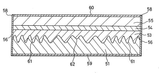
Figure 2 is a cross-sectional view showing a single
wavelength oscillating semiconductor laser device in
accordance with a second embodiment of the present invention.
:
2023~10
In Figure 2, an n type InGaAsP guide layer 53, an InGaAsP
active layer 54 and a p type InP clad layer 55 are
sequentially formed on an n type InP substrate 51 where a
primary diffraction grating 61 and a secondary diffraction
grating 62 are formed, the latter having a phase shift region
62a in the center thereof, An n side electrode 59 is provided
on a back surface of the substrate 51 and a p side electrode
60 is provided on the p type InP layer 55. A nonreflective
coating film 58 is provided on both facets of the laser.
Next, operation of the single wavelength oscillating
semiconductor laser in accordance with this embodiment will
be described.
A beam is more effectively reflected by a low
ordered diffraction grating. Therefore, as shown in Figure
2, when the order of the diffraction grating 62 located in the
center of the element is higher than that of the diffraction
grating 61 in the neighbourhood of resonator facets, the
reflection intensity of the beam in the center of the element
is less than that in the neighbourhood of the resonator
facets. As a result, the beam generated at the active layer
54 is not confined only in the center of the element and most
beams will advance to the neighbourhood of the resonator
facets and then be reflected by the diffraction grating 61.
Therefore, the beam density is not high only in the center of
the element and is uniform over the whole element, with the
result that hole burning is not likely to occur and as a
result it is possible to provide a single wavelength
oscillating semiconductor laser device having highly linear
beam output with respect to the injection current, and highly
stable single wavelength oscillation. In addition, the laser
beam can be outputted in the vertical direction to the
substrate by the secondary diffraction grating 62 in this
laser device.
Meanwhile, according to the conventional method for
manufacturing the diffraction grating shown in Figure 8, since
a diffraction grating having the same cycle is formed over the
-- 10 --
.
2023510
whole surface of the substrate, it is not possible to form a
semiconductor laser having the primary and secondary
diffraction gratings shown in Figure 2.
According to a method for manufacturing a
diffraction grating in accordance with the present invention,
a diffraction grating having two different cycles can be
formed at the same time on the same planar surface by one
interference exposure.
This method for manufacturing the diffraction
grating in accordance with the third embodiment of the present
invention will be described hereinafter with reference to
Figures 3(a) to 3(e).
Figures 3(a), 3(b), 3(d) and 3(e) are cross-
sectional views showing the manufacturing steps of a
diffraction grating in accordance with a third embodiment of
the present invention and Figure 3(c) is a diagram showing
distribution of beam intensity.
The manufacturing steps of the diffraction grating
in accordance with the embodiment will be described
hereinafter.
First, referring to Figure 3(a), the variable speed
resist (image reversible resist) 42, is applied to the
substrate 31 where the diffraction grating is to be formed,
is then, baked at a temperature of llO to 120 C for five
minutes so that the developing speed will have the minimum
value with respect to a predetermined exposure intensity.
Referring to Figure 3~b), the semi-transparent mask 43 is then
partially arranged on the resist 42 and then by a two-beam
interference exposure method, the resist 42 is exposed with
exposure intensity in which the maximum and minimum values of
the exposure intensity are on both sides of the predetermined
intensity which causes the minimum developing speed. The
portion which is not covered with the semi-transparent mask
43 and exposed with exposure intensity in which the maximum
value of the exposure intensity is less than the intensity
which makes the developing speed to be the minimum value in
-- 11 --
2023~10
a portion covered with the semi-transparent mask 43. Figure
3(c) is a diagram showing distribution of the beam intensity
at this time. Then, referring to Figure 3(d), the resist 42
is developed so that the portions of the resist 42 exposed to
S the beam intensity which causes the minimum developing speed
are left and patterned to form a diffraction grating 45a.
Then, referring to Figure 3(e), the substrate 31 is etched
away with an appropriate etchant such as a HBr/HNO3/H2O mixed
solution, a HBr/HNO3/CH3OH mixed solution or a Br2/CH3OH mixed
solution using the patterned resist 42 as a mask to form a
diffraction grating 45b.
As described above, when the image reversible resist
is exposed so that the maximum value of the exposure intensity
by the interference exposure is more than the point at which
the developing speed has the minimum value (value ~ in Figure
5) and the minimum value of the exposure intensity is less
than the value ~, the resist can be developed so that the
resist at portions exposed with the intensity which causes the
developing speed to be the minimum value are left. As a
result, after etching, it is possible to form a diffraction
grating having a cycle which is a half of the cycle of an
interference fringe obtained by the interference exposure
method. Meanwhile, when the maximum value of the exposure
intensity by the interference exposure is less than the
minimum value point ~ of the exposure intensity is more than
the value ~, the resist i8 left in a cycle of an interference
fringe obtained by the interference exposure, whereby a
diffraction grating having the cycle of the interference
fringe is formed.
Therefore, in cases where a portion of the substrate
is covered with the semi-transparent mask, when the maximum
value of the exposure intensity in the portion which is not
covered with the mask i8 greater than the value a and the
minimum value thereof i6 less than the value ~ and, the
maximum value of the exposure intensity in the portions
covered with the mask is less than point ~, diffraction
- 12 -
., ~
, .: ,, ~ .
2023~10
gratings having cycles of ~ and A/2 by one interference
exposure at the same time are possible.
Next, a description will be given of the
manufacturing steps of a semiconductor laser device shown in
Figure 4, which has primary and secondary diffraction gratings
like the semiconductor laser device shown in Figure 2 by using
the method for manufacturing the diffraction grating in
accordance with this embodiment.
Similar to the semiconductor laser shown in Figure
2, the semiconductor laser shown in Figure 4 comprises primary
and secondary diffraction gratings 76 and 75 formed on a
substrate 71, in which a phase shiPt region is not formed in
the center of the secondary diffraction grating 76. Referring
to Figure 4, a p type InGaAsP guide layer 72, an InGaAsP
active layer 73 and an n type InP clad layer 74 are
sequentially formed on a p type InP substrate 71 where the
primary and secondary diffraction gratings 76 and 75 are
formed. The electrodes and coatings on the facets are not
shown.
The diffraction gratings are manufactured on the p
type InP substrate 71 instead of the substrate 31 shown in
Figure 3 in accordance with the process shown in Figure 3.
More specifically, first, referring to Figure 3(a), the resist
(image reversible resist), is applied to the substrate, and
is then baked at a temperature of 110 to 120 C. Referring
next to Figure 3(b), the substrate i8 partially covered with
a semi-transparent mask 43 and then the resist i8 exposed by
the interference exposure method with an exposure intensity
in which the maximum and minimum values are on both sides of
the predetermined minimum developing speed (~) intensity which
makes the portion which is not covered with the semi-
transparent mask 43 and exposed with exposure intensity in
which the maximum value of the exposure intensity is less than
the predetermined minimum developing speed intensity in the
portion covered with the semi-transparent mask 43. In this
embodiment, the width of the semi-transparent ma~ks 43 and
- 13 -
.
i,, ,,, ~
~02~510
distance between them are approximately 300 microns.
Thereafter, the substrate is etched away using an appropriate
etchant to form the diffraction gratings 75 and 76. Then, the
InGaAsP guide layer 72 having a composition ratio of which
permits the layer to have a band gap corresponding to a
wavelength of 1.15 microns, the InGaAsP active layer 73 having
a composition ratio of which permits the layer to have a band
gap corresponding to a wavelength of 1. 3 microns, and the n
type InP clad layer 74 are sequentially formed and then
divided into a chip in the center of the primary diffraction
grating by cleavage. Thus, a DFB laser shown in Figure 4 is
completed.
Although a semiconductor laser having no phase shift
region was described in the above embodiment, when a phase
shift plate is introduced into the interference exposure
apparatus, the phase shift region can be formed in the center
of the element in accordance with the manufacturing method of
the diffraction gratings in accordance with the present
invention. As a result, the semiconductor laser device shown
in Figure 2 can be manufactured.
In addition, although the diffraction grating with
a cycle of ~ i8 formed in the portion covered with the semi-
transparent mask and the diffraction grating with a cycle of
A/2 is formed in the portion not covered with the semi-
transparent mask in the above embodiment, the same effect canbe attained even if the whole surface of the resist on the
substrate is exposed before or after the interference exposure
so that the maximum value of the exposure intensity is more
than the value ~ and the minimum value thereof is less than
value ~ in the portion covered with the semi-transparent mask
and the minimum value of the exposure intensity is more than
the value ~ in the portion which i8 not covered with the mask.
As described above, according to the present
invention, the method for manufacturing the diffraction
grating comprises the steps of applying a resist, of which
developing speed has the extreme value with respect to certain
- 14 -
2023510
exposure intensity, to a substrate where the diffraction
grating is to be formed, performing interference exposure with
beam intensity in which the maximum and minimum values of the
exposure intensity may be on both sides of intensity which
makes the developing speed to be the extreme value and etching
the sub~trate using a pattern, which is obtained by developing
the resist, as a mask. Thus, a diffraction grating pattern
having a cycle which is a half of an interference fringe
obtained by an interference exposure method can be formed.
In addition, according to the present invention,
since the order of the diffraction grating in the center of
an element is higher than that of the diffraction grating in
the neighbourhood of resonator facets in a semiconductor laser
device having the diffraction grating in an active region,
beam density is prevented from being increased in the center
of the element and very linear beam output with respect to
injection current and highly stable single wavelength
oscillation can be obtained.
In addition, according to the present invention, the
method for manufacturing the diffraction gratings comprises
the steps of applying a resist, of which developing speed has
the extreme value with respect to certain exposure intensity,
to a substrate where the diffraction grating is to be formed,
partially covering the resist with a semi-transparent mask,
performing an interference exposure with beam intensity in
which the maximum and minimum values of the exposure intensity
are on both sides of intensity which makes the developing
speed to be the extreme value in either a portion covered with
the semi-transparent mask or another portion and etching the
substrate using a pattern, which is obtained by developing the
resist, as a mask. As a result, two kinds of diffraction
gratings having different cycles are formed by one
interference exposure at the same time and the semiconductor
laser having the primary and secondary diffraction gratings
can be easily formed.
- 15 -
`:
,, j,...
2023sla
Although the present invention has been described
and illustrated in detail, it is clearly understood that the
same is by way of illustration and example only and is not to
be taken by way of limitation, the spirit and scope of the
present invention being limited only by the terms of the
appended claims.
- 16 -
~:.