Note: Descriptions are shown in the official language in which they were submitted.
~. ~ 1 2023605
PROTECTION CIRCUIT PROTECTED FROM
OVERVOLTAGE OR OVERCURRENT
The present invention relates to a circuit for protectirlg a
semiconductor circuit or a telephone line from a lightning surge and overvoltageor overcurrent. In particular, it relates to a circuit using a surge absorber for
protecting the semiconductor circuit or the telephone line from a lightning surge,
5 as well as from continuous overvoltage or overcurrent which may be generated
by a short-circuit in an alternating-current electric source or other power source.
Protection circuits have been used for protecting equipment such
as a communication line, e.g. a telephone line for a telephone and telecopier,
and a line for cable television and cable radio and the like, from a lightning
10 surge and overvoltage or overcurrent. The protection circuit includes a fuse or
a low-melting-point metallic wire in combination with an element for absorbing
a surge from, for instance, an arrestor or a varistor. When a surge caused by,
for example, lightning is generated, protection of the semiconductor circuit is
attained by maintaining a level of voltage below a response voltage of the
15 surge-absorbing element. This corresponds to a voltage for starting electrical
discharge in a case where the element is formed by the arrestor, and to a
varistor voltage in a case where the element is formed by the varistor.
For an overvoltage or overcurrent, a fuse is provided which is
broken by an electric current generated in the fuse itself or by heat generated
20 by the surge-absorbing element. The circuit is opened and thereby protected.
For an overvoltage or overcurrent, neither the surge-absorbing
element nor the fuse can operate in the case where the value of the voltage is
lower than the response voltage value of the element and where the value of
the electric current is lower than the breaking current value of the fuse,
25 respectively. Thus the circuit stays closed, and the protection of the circuit
cannot be realized.
In the case of recent semiconductor circuits, a Zener diode has
been connected in parallel to the circuit in order to attain protection thereof. In
this case, all of any overcurrent generated is directed into the Zener diode, and
2023605
the surge-absorbing element does not operate properly. This causes the Zener
diode to become overheated by an electric current below that creating a melting
temperature.
In other words, heretofore, protective networks for protecting
5 equipment from overvoltages have employed a spark-gap surge-absorbing
element to shunt overvoltage and excessive currents from the input conductor
to ground, and have further employed a series-connected fuse for disconnecting
or open-circuiting the source of overvoltage or current from the equipment to beprotected. Such a protective network is described in U.S. Patent Nos.
3,448,341 and 3,795,846, and in NASA Tech. Brief No. 69-10490, October,
1969.
Further, there have been published in laid-open Japanese Patent
Publication Nos. 63-99725, 63-205026/1988 and 64-77426/1989 measures to
resolve the case in which a short-circuit occurs in a source, such as for instance
15 an alternating current source of 600 volts. Each publication discloses a
respective method of preventing overheating and burning of a surge-absorbing
element. They involve opening of a circuit by melting of a fuse, or by contact
between a low-melting-point metal wire and the surface of a microgap surge-
absorbing element in which heat generated by an overvoltage or overcurrent
20 charge in the surge-absorbing element melts the low-melting-point wire, thereby
opening the circuit.
In the above-mentioned methods, because a fuse is fused or a
low-melting-point metal wire is melted, a telephone or a cable television is notable to be used after the short-circuit condition ends. The fuse or low-melting-
25 point metal wire must be replaced, and the microgap surge-absorbing element
may also need to be replaced.
Many attempts have been made to resolve these problems in a
protection circuit for protecting a communication line, telephone switchboard and
similar equipment from a lightning surge and overvoltage or overcurrent, i.e.
30 protecting without needing to replace the element(s) after the circuit is opened.
C-
2023605
With the foregoing considerations in mind, the present invention
contemplates the provision of an improved protection circuit.
It is an object of the present invention to provide a circuit for
protecting a semiconductor circuit or a telephone line from a surge such as a
5 lightning surge and overvoltage or overcurrent.
It is another object of the present invention to provide a protection
circuit which can protect without opening the circuit when a telephone line is
charged with overvoltage or overcurrent, for example, by contacting an electric
source.
It is a further object of the present invention to provide a protection
circuit which will generate neither burning nor overheating at the microgap
surge-absorbing element, even when the line to be protected is charged with
overvoltage or overcurrent, i.e. through a short-circuit with the electric source.
Figure 1 shows schematically a prior art protection circuit for
experimenting with a short-circuit in an electric source.
Figure 2 shows schematically a protection circuit according to the
present invention, which comprises a microgap surge-absorbing element
arranged in parallel with a telephone, and a positive-resistance-temperature-
coefficient thermistor in series with the telephone.
Figure 3 shows schematically a structure for experimenting with a
short-circuit of the protection circuit of the present invention, the structure having
a source with a controlling resistor.
Figures 4 and 5 show other embodiments of the protection circuit
in accordance with the present invention.
In accordance with the present invention, a protection circuit for
protecting communication equipment or a semiconductor circuit has an electrical
source connected to the equipment or circuit for supplying current to the
equipment or the circuit. It also has a surge-absorbing device arranged in
parallel with the equipment or the circuit, for absorbing a surge from said
electrical source to the equipment or the circuit. It further has a positive
thermistor having a high positive-resistance-temperature coefficient, arranged
4 2023605
in series with the equipment or the circuit, at a position between the electric
source and the surge-absorbing means, and a resistor connected in series with
the semiconductor circuit or the line, at a position between the thermistor and
the electric source.
Preferably, the thermistor used has a switching temperature of
between 65C and 165C. Also preferably, the thermistor has a nominal zero-
changing resistance value at a value lower than 1 kilo-ohm.
In accordance with the present invention, the current flowing
through the protection circuit can be restricted, without the circuit being opened
by the melting of a fuse or a low-melting-point metal wire as in the prior art
protection circuit.
A surge-absorbing element is arranged in parallel with the
equipment to be protected, and a positive thermistor is connected in series to
both that equipment and the surge-absorbing element, forming a protection
circuit. Therefore, the protection circuit can be opened without any fuse and
without melting (irreversible dissolution) of a fuse or a low-melting-point metal
wire when overvoltage or overcurrent is applied to the equipment. In other
words, the electric current flowing through the protection circuit (the microgapsurge-absorbing element) can be suppressed by operating the positive
thermistor so as to avoid overheating and firing of the circuit and the substrate.
The combination of the microgap surge-absorbing element and the
thermistor allows correct control of the circuit.
A positive thermistor for the invented protection circuit is a thermo-
sensing element capable of increasing drastically the resistance value with an
increase in the circumstantial temperature, i.e. a thermistor having positive-
temperature-resistance-coefficient characteristics.
When the temperature of the element is raised, the resistance of
the element is increased, and then the element has a switching property.
Excessive current flowing through the positive thermistor heats it to increase
drastically the resistance value thereof. The inventive protection circuit utilizes
this feature of the positive thermistor.
1 ~
20236n5
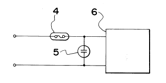
The protection circuit of the present invention has the structure
shown in Figure 2. A surge-absorbing element 5 is arranged in parallel with a
telephone 6, and a positive thermistor 4 is connected in series with the
telephone 6. When an overvoltage of AC 600 V is connected to the terminals
3 of the circuit, the microgap surge-absorbing element 5 is discharged and the
overvoltage current simultaneously flows through the positive thermistor 4. The
overvoltage current flowing through the positive thermistor 4 drastically raisesthe resistance value of the positive thermistor, and then the current flowing
through the microgap surge-absorbing element decreases below the current
value that generates overheating, thereby avoiding such overheating and
burning of the surge-absorbing element.
Such a positive thermistor preferably has a switching temperature
of between 60C and 165C. When the switching temperature is below 65C,
the protection circuit operates at the usual temperature of the equipment being
protected. If the switching temperature exceeds 165C, the heat generated can
affect the resin of the substrate, and the circuit substrate can be damaged.
Such a positive thermistor preferably has a nominal zero-change
resistance value lower than 1 kilo-ohm. When the nominal zero-change
resistance value exceeds one kilo-ohm, excessive energy loss can occur and
the circuit and the equipment can be affected.
The present invention is further illustrated by the following
examples, which illustrate the inventive circuit and a short-circuit condition. The
examples should not, however, be interpreted to limit the invention.
EXAMPLE 1
Figure 3 shows an embodiment of the protection circuit of the
invention, and an experimental structure for creating a short-circuit using an
electrical source with a controlled resistor.
A microgap surge-absorbing element 5 with a direct-current
discharging voltage of 400 V is arranged in parallel with a telephone set 6, anda positive thermistor 4 with nominal zero-changing resistance of 8 ohms and a
~C
2023605
switching temperature of 80C is arranged in series with the telephone set 6
and the surge-absorbing element 5.
Connectors 3 shown in Figure 3 are arranged to connect an AC
source (AC 600 V) 1 through a controlling resistor (15 ohms) 2 with the
5 protection circuit to be tested.
As a comparison circuit, a protection circuit as shown in Figure 1
using a surge-absorbing element 15 was tested in a similar configuration to thatshown in Figure 3. This comparison circuit comprises a microgap surge-
absorbing element 15 having a direct-current discharging voltage of 400 V
10 adjacently provided with a low-melting-point melt wire 14 with a melting point of
410C. The source 11 with a controlling resistor 12 of 15 ohms provides an
alternating current with 600 V maximum voltage.
The above-mentioned two species of protection circuit were tested
by using a charging overvoltage of 600 V. The result is described below.
In the protection circuit shown in Figure 1 the low-melting-point
wire fused 35 milliseconds after charging with overvoltage (being connected to
the source 11); the circuit was opened without burning of the surge-absorbing
element.
In the inventive protection circuit shown in Figure 3, the current
20 value flowing through the microgap surge-absorbing element decreased
drastically from 1.7 A to 0.01 mA at about 20 milliseconds after charging with
overvoltage (i.e. after connecting with the source), and then the charging
continued for 10 minutes, but no overheating or burning was found in the circuitstructure. Further, after the charging was discontinued, the protection functions
25 of the positive thermistor and the microgap surge-absorbing element were
recovered, and their operative characteristics were not changed.
EXAMPLE 2
Figure 3 shows an embodiment of the protection circuit of the
invention, and an experimental structure for creating a short-circuit using an
30 electrical source with a controlled resistor.
7 2023605
A microgap surge-absorbing element 5 with a direct-current
discharging voltage of 400 V is arranged in parallel with a telephone set 6, anda positive thermistor 4 with nominal zero-changing resistance of 8 ohms and a
switching temperature of 80C is arranged in series with the telephone set 6
5 and the surge-absorbing element 5.
Connectors 3 shown in Figure 3 are arranged to connect an AC
source (AC 600 V) 1 through a controlling resistor (275 ohms) 2 with the
protection circuit to be tested.
As a comparison circuit, a protection circuit as shown in Figure 1
10 using a surge-absorbing element 15 was tested in a similar configuration to that
shown in Figure 3. This comparison circuit comprises a microgap surge-
absorbing element 15 having a direct-current discharging voltage of 400 V
adjacently provided with a low-melting-point melt wire 14 with a melting point of
410C. The source 11 with a controlling resistor 12 of 275 ohms provides an
15 alternating current with 600 V maximum voltage.
The above-mentioned two species of protection circuit were again
tested by using a charging overvoltage of 600 V. The result is described below.
In the protection circuit shown in Figure 1 the low-melting-point
wire fused 2 to 3 seconds after applying the overvoltage (i.e. after connecting
20 to the source 11 ); the circuit was opened without burning of the surge-absorbing
element.
In the inventive protection circuit shown in Figure 3, the current
value flowing through the microgap surge-absorbing element decreased
drastically from 1.8 A to 0.005 mA about 0.5 seconds after applying the
25 overvoltage (i.e. after connecting with the source), and then the charging
continued for 10 minutes, but no overheating or burning was found in the circuitstructure. Further, after the application had continued for 30 minutes and was
then discontinued, the protection functions of the positive thermistor and the
microgap surge-absorbing element were recovered, and their operative
30 characteristics were not changed.
-'
8 20236~)5
EXAMPLE 3
Figure 3 shows an embodiment of the protection circuit of the
invention, and an experimental structure for creating a short-circuit using an
electrical source with a controlled resistor.
A microgap surge-absorbing element 5 with a direct-current
discharging voltage of 400 V is arranged in parallel with a telephone set 6, anda positive thermistor 4 with nominal zero-changing resistance of 8 ohms and a
switching temperature of 80C is arranged in series with the telephone set 6
and the surge-absorbing element 5.
Connectors 3 shown in Figure 3 are arranged to connect an AC
source (AC 600 V) 1 through a controlling resistor (15 ohms) 2 with the
protection circuit to be tested.
As a comparison circuit, a protection circuit as shown in Figure 1
using a surge-absorbing element 15 was tested in a similar configuration to thatshown in Figure 3. This comparison circuit comprises a microgap surge-
absorbing element 15 having a direct-current discharging voltage of 400 V
adjacently provided with a low-melting-point melt wire 14 with a melting point of
410C. The source 11 with a controlling resistor 12 of 15 ohms provides an
alternating current with 600 V maximum voltage.
In the protection circuit shown in Figure 1 the low-melting-point
wire fused 35 milliseconds after charging the overvoltage (i.e. after connectingto the source 1 1 ); the circuit was opened without burning of the surge-absorbing
element.
In the inventive protection circuit shown in Figure 3, the current
value flowing through the microgap surge-absorbing element decreased
drastically from 1.7 A to 0.01 mA about 30 milliseconds after charging the
overvoltage (i.e. after connecting with the source), and then the charging
continued for 10 minutes, but no overheating or burning was found in the circuitstructure. Further, after the charging had continued for 10 minutes and was
then discontinued, the protection functions of the positive thermistor and the
C
9 2023605
microgap surge-absorbing element were recovered, and their operative
characteristics were not changed.
EXAMPLE 4
Figure 4 shows another embodiment of the protection circuit of the
invention.
The protection circuit shown in Figure 4 is connected to an AC
source (AC 600 V) 1 through a controlling resistor (15 ohms) 2.
The overvoltage currents applied to the circuit can flow separately
through each of the thermistors 4 and through discharging paths to the surge-
absorbing element 5 to the ground, so as to protect the equipment 6. The
overcurrent flows through the central electrode of the two-electrode surge-
absorbing element 5.
Further, after the charging was discontinued, the protection
functions of the positive thermistor and the microgap surge-absorbing element
were recovered, and their operative characteristics were not changed.
EXAMPLE 5
Figure 5 shows a still further embodiment of the protection circuit
of the invention.
In this protection circuit, the overvoltage currents applied to the
circuit can flow respectively through each of the thermistors 4 and the surge-
absorbing elements 5 to the ground.
The inventive protection circuit for protecting a communication line
from both a lightning surge and overvoltage or overcurrent provides the
following significant effects:
Firstly, it can restrict the overvoltage current to similar values to
the prior art protection circuit against the overvoltage and overcurrent appliedto the microgap surge-absorbing element.
Secondly, it can avoid burning and overheating of the surge-
absorbing element, and can also avoid burning of communication equipment.
.~
2023605
Thirdly, the protection circuit protects the equipment without
opening the circuit, and the equipment can then be used immediately after the
overvoltage discontinues.
Further, the circuit can be repeatedly used without any
5 replacement of parts, thereby providing a practical and inexpensive protection circuit.
The advantage of the protection circuit of the present invention is
that it provides both personal and equipment protection from overvoltage and
overcurrent which exceeds the fuse-rating or the destructive voltage rating of the
10 surge-absorbing element. Its simplicity results in a large cost reduction over
other methods. In addition, the protection circuit is passive except for the
condition of overload; therefore, it results in no need for calibration.