Note: Descriptions are shown in the official language in which they were submitted.
2023642
ELECTRICAL DOUBLE-LAYER CAPACITOR
The present invention relates to an electrical
double-layer capacitor wherein the contact resistance between
the collecting electrode and the sintered polarising electrode
has been made small.
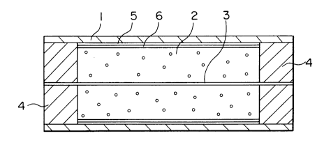
A conventional electrical double-layer capacitor
cell is shown in Fig. 4. In Fig. 4, numeral 1 denotes a
collecting electrode, 2 a sintered polarising electrode, 3 a
separator, 4 a gasket, and A the contact part of the collector
electrode 1 and the sintered polarising electrode 2.
For the collector electrode 1, a conductive rubber
sheet can be used and for the gasket 4 a non-conductive rubber
can be used. Also a polypropylene porous film can be used for
the separator 3.
The sintered polarising electrode 2 is one which is
made of active carbon particles formed in a solid plate-like
shape and in which is impregnated an electrolytic liquid
(example, dilute sulfuric acid). A different type of
electrode 2 is known which is brought into a paste-like form
by mixing active carbon particles and the electrolytic liquid.
However, the present invention relates to an electrical
double-layer capacitor cell which uses a polarising electrode
made into a solid plate-like shape by sintering in the manner
as described above.
The gasket 4 is made in a tube-like shape, and a
separator 3 is arranged approximately centrally thereof to
separate upper and lower parts. Then, the sintered polarising
electrode 2 fills the upper and lower sides of the separator
3. A collecting electrode 1 is provided in such a manner as
to cover the upper and lower surfaces of the sintered
polarising electrode 2 and the gasket 4.
The gasket 4 is adhered to the collecting electrode
1 and the separator 3, and the collecting electrode 1 is made
to contact the surface of the sintered polarising electrode 2.
The above-described adhesion is carried out by the use of an
adhesive agent or the use of a heat melting process.
'~
202364;~
-
Such an electrical double-layer capacitor cell is
known, for example, from Japanese Patent Application Laid-Open
No. 8753/1974 and No. 292612/1987.
However, a problem associated with the electrical
double-layer capacitor cell using the above-described sintered
polarising electrode 2 is that the contact resistance at the
contact part A of the collecting electrode 1 and the sintered
polarising electrode 2 is relatively high.
When the surface of the sintered polarising
electrode 2 is seen at a microscopic level, it is uneven and
active carbon particles are protruding at various points. On
the other hand, the collecting electrode 1 is a rubber sheet
wherein conductive particles are contained therein.
When both surfaces are brought into contact, the
electrical resistance becomes small at the position where the
protruding parts of the active carbon particles of the
sintered polarising electrode 2 make contact with the
conductive particles of the collecting electrode 1. However,
at other regions where such contact does not happen, the
electrical resistance becomes large. Due to this fact, the
contact resistance of the whole contact part A cannot be made
small at any rate.
The present invention has the object of solving the
problem described above.
The object of the present invention is to diminish
the resistance of the contact part of the collecting electrode
and the sintered polarising electrode in an electrical double-
layer capacitor cell.
In order to attain the above-described object, in
the present invention, there is provided an electrical double-
layer capacitor cell, in which the collecting electrode and
the sintered polarising electrode are contacted via conductive
metallic evaporated films formed on respective surfaces.
These and other objects of the invention will become
more apparent in the detailed description and the following
figures in which:
2023642
Fig. 1 is a diagram showing the electrical double-
layer capacitor cell according to an
embodiment of the present invention;
Fig. 2 is a diagram showing the collecting
electrode evaporated with a conductive
metal;
Fig. 3 is a diagram showing a sintered polarising
electrode evaporated with a conductive
metal; and
Fig. 4 is a diagram showing a conventional
electrical double-layer capacitor cell.
Fig. 1 shows an electrical double-layer capacitor
cell according to an embodiment of the present invention. The
reference numerals correspond to those of Fig. 4. Numeral 5
denotes a conductive metallic evaporated film formed on the
surface of the collecting electrode 1, and numeral 6 denotes a
conductive metallic evaporated film formed on the surface of
the sintered polarising electrode 2.
The conductive metal to be evaporated can be any one
of the following metals: gold (Au), silver (Ag), platinum
(Pt), copper (Cu), nickel (Ni), etc. The evaporation is
carried out by use of a vacuum evaporation equipment. The
metal to be evaporated is put on an evaporating source
filament or in a boat, and evaporation is carried out in a
vacuum at an atmosphere of 5 x 10⁻⁴ to 5 x 10⁻⁵ mm Hg. The
evaporated film may be formed only on the part where the
collecting electrode 1 and the sintered polarising electrode 2
are in contact.
Since the conductive metallic evaporated film 5
firmly adheres to the active carbon particles of the surface
of the collecting electrode 1, the electrical resistance
between the active carbon particles and the conductive metal
evaporated film 5 is negligibly small. The electrical
resistance between the conductive particles on the surface of
the sintered polarising electrode 2 and the conductive metal
evaporated film 6 is similarly small. Also, the conductive
metal evaporated films 5 and 6 provide generally smooth
surfaces.
- 3 -
. ~ ,,
2023642
As a result of the fact that the conductive metal
evaporated film has been formed in the manner described above,
the collecting electrode 1 and the sintered polarising
electrode 2 have a smooth and uniformly extended conductive
metal film on the surface of the contact part thereof. Since
the contact between the collecting electrode 1 and the
sintered polarising electrode 2 is carried out using
conductive metal films, the contact resistance becomes
extremely small.
- 4 -
~,.