Note: Descriptions are shown in the official language in which they were submitted.
FIELD OF THE INVENTION
The present invention relates to an apparatus for
forming a thin film by chemical vapor deposition
(abbreviated as "CVD" hereinafter). More particularly, the
05 present invention is concerned with a chemical vapor forming
apparatus suitable for forming a thin film of diamond,
silicon, silicon dioxide, alumina, silicon carbide, silicon
nitride, boron nitride and so forth.
DESCRIPl'ION OF THE RELATED ART
In recent years, thin films of diamond, silicon and so
forth are finding increasing applications in various fields
such as semiconductors, tools, machine parts, composite
materials, nuclear plant components, and so on.
Conse~uently, the increase in applications has
necessitated the need for higher ~uality films with
dimensional stability. Many studies have been made for
development of techniques for obtaining thin films of
uniform quality and thickness.
For instance~ in case of vapor deposition of diamond,
various methods have been proposedr for example, a hot
filament CVD method disclosed in Japanese Examined Patent
Publication No. 59-27753, a plasma CVD method of substrate
heating type as disclosed in Japanese Unexamined Patent
Publication No. 58-156594, a microwave plasma CVD method as
disclosed in Japanese Examined Patent Publication No. 59--
27754, and a cooling microwave plasma CVD method disclosed
in Japanese Examined Patent Publication No. 62-21757.
2~?~3~
Meanwhile, Kaneko et al. discloses the production of
thin films by methods of hot filament typer substrate
heating type and cooling typel at pp 546-552, Applied
Surface Science Vol 33/34 (1988).
05 In the hot filament method disclosed in Japanese
Examined Patent Publication No~ 59-27753, a filament is
heated to about 2000C so as to decompose a source gas
thereby producing active species which contribute to
deposition of diamond. It is therefore necessary that a
substrate is disposed within the reach of the active
species. Usually, a hot filament is disposed at a position
which is several millimeters from the substrate, so that the
substrate receives a large quantity of heat radiated from
the filament. It is therefore extremely difficult to
maintain a given constant temperature of the substrate
surface.
The microwave plasma CVD method disclosed in Japanese -~
Examined Patent Publication No. 59-27754 has difficulty in
accurately controlling the substrate temperature, because
the substrate temperature varies due to various factors
including variations in the characteristics of plasma and
variations ln the configuration and material of the
substrate.
rrhe microwave plasma CVD method disclosed in Japanese
Unexamined Patent Publication No. 58-156594 is intended to
obviate the problems mentioned above, and employs means for
heating the substrate thereby to control the substrate
temperature. This method, relying upon positive heating of
the substrate, can effectively be applied to the microwave
plasma CVD method in which the substrate receives only a
small quantity of heat from the substrate, but is not
suitable in other methods in which the substrate receives a
05 large quantity of heat, such as the hot filament CVD method,
plasma jet method and combustion flame method.
~ apanese Examined Patent Publication No. 62-21757
proposes a CVD method in which the substrate temperature is
controlled by cooling the substrate using a coolant. This
method, however, is unsatisfactory in that the substrate
temperature is controllable only over a limited range and in
that the temperature control cannot be conducted with a good
response.
Thus, all these known CVD methods suffer from
lS disadvanta~es in that the substrate temperature is
controllable only in a limited temperature range and in that
the temperature control cannot be effected with good
response. It is understood that a t:echnique for controlling
the substrate temperature is quite an important factor in
the vapor deposition of diamond, for which no technique has
been established for satisfactorily controlling the
substrate temperature.
SUMMARY OF THE INVENTION
Accordingly, an object of the present invention is to
provide a chemical vapor deposition apparatus for forming a
thin film, capable of overcoming the above-described
problems of the prior art.
73461-16
One aspect of the present invent.ion provides an appara-
tus for forming, by chemical ~apor deposition, a thin ~ilm on
the surface of a heated substrate placed in a vessel, the
apparatus comprising:
gas supplying and exhausting means for supplying a
source gas into the vessel and exhausting the gas from the vessel;
decomposing means for decomposing the source gas;
substrate supporting means for supporting the substrate;
substrate cooling means for cooling the substrate;
substrate heating means for heating the substrate;
subskrate temperature measuring means for measuring
the temperature of the substrate; and
substrate temperature control means for controlling the
temperature of said substrate.
In one preferred embodiment of the apparatus, the
substrate heating means includes a heating electric power supply
and power supply electrodes, and the substrate supporting means
includes the power supply electrodes and the substrate cooling
means, arranged such that the substrate is supported between :.. -. l ,
the power supply electrodes and the substrate coolin~ means,
with an insulating means for insulating the. substrate cooling
means from ~h~ substrate and the power supply electrodes, where-
by the substrate is directly heated by the heat generated in the
substrate by an electric current supplied through the power supply
electrodes.
In another preferred embodiment of the apparatus, the '
- ~ : , , .
, . .
.:
73461-16
substrate heating means includes a heating electric power supply
and power supply electrodes, the power supply electrodes including
-the substrate cooling means. -
In yet another preferred embodiment of the apparatus,
the substrate temperature measuring means measures, in a non-
contacting manner, the temperature of the surface of the substrate
which is opposite to the substrate surface on which the film is
formed.
In a still preferred embodiment of the apparatus, the
thin film is made of diamond.
Arlother aspect of the present invention provides a
process for forming a thin film, comprising the steps of:
providing a substrate in a vessel;
heating the substrate;
supplying a source gas to the vessel, decomposing the
source gas, and exhausting the resultant gas ~rom the ~essel;
depositing a thin film on the substrate by chemical ~ .
vapor deposition while simultaneously heating and cooling the
substrate,
measuring a temperature of the substrate and
varying the heating in response to the temperature.
In one preferred embodiment of the process the heating
is conducted by electric power and the cooling is conducted by
water.
In another preferred embodiment of the process, during
the deposition, the temperature is maintained substantially
- 5a -
A
73~61-16
constant.
BRIEF DESCRIPTION OF THE DRA~INGS
Figure 1 is a sehematic illustration of an embodiment
of a chemical vapor deposition apparatus of the invention for
~orming a thin filmî
:: Figure 2 is a sehematic perspective view of a substrate
supporting device with a temperature eontroller, used in another
embodiment of the present invention;
~ Figure 3 is a schematle illustration of an electrie
: 10: power supply holder with a temperature controller, used in still
another embodiment of the present lnvention)
`'"
..
,~, ,,:
''
- 5b -
: . . . . . . .
~.
~ ~3 ~ ~a ~
Fig. 4 is a schematic perspective view of another
example of the power supply holder of the present invention;
and
Fig. 5 is a diagram showing the relationship between
05 the substrate temperature and the growth rate and the
quality of the diamond thin film.
DESCRIPTION OF T~E PREFERR~D EMBODIMENTS
The invention will be described in more detail with
reference to the drawings.
Fig. 1 is a schematic illustration of an embodiment of
the apparatus of the present invention, applied to a system
for forming a thin film by chemical vapor deposition
employing a hot filament.
The present inventors have discovered the following
facts in the course of a further study. Namelyr the
inventors have found that a relationship as shown in Fig.5
exists between the substrate temperature and the rate of
growth of diamond, as well as the quality of the crystal.
In Fig. 5, the quality of the crystal is expressed in
terms of a ratio Ind/Id between the pea~ intensity Ind of
non-diamond carbon as impurity and the peak intensity Id of
diamond, the peak intensities being determined through Raman
spectral analysis of the deposited diamond. Thus, a
smaller value o~ the ratio Ind/In indicates better quality
of the diamond crystal.
From Fig. 5~ it is understood that the growth rate and
the purity of the diamond can be freely controlled by
suitably setting the substrate temperature. For instance, a
$ ~
diamond of a high purity can be deposited at a low substrate
temperature TA, whereas deposition at a substrate
temperature TB enables diamond to deposit at a high growth
rate although the purity is slightly reduced. Thus, in the
05 CVD process for depositing diamond, it is necessary that the
substrate temperature is controlled over a wide range and
with good accuracy, in order to obtain a desired quality and
growth rate of crystalO
For instance~ when the substrate temperature which has
been maintained at TA during deposition is shifted to a
higher temperature for any reason~ the purity of the diamond
is seriously decreased. Conversely, when the substrate
temperature is shifted to a lower temperature from TB during
the deposition, the crystal growth rate is lowered to make
it impossible to obtain the required amount of deposition
within a given time. Thus, minimization of fluctuation of
the substrate temperature during deposition also is a very
important factor
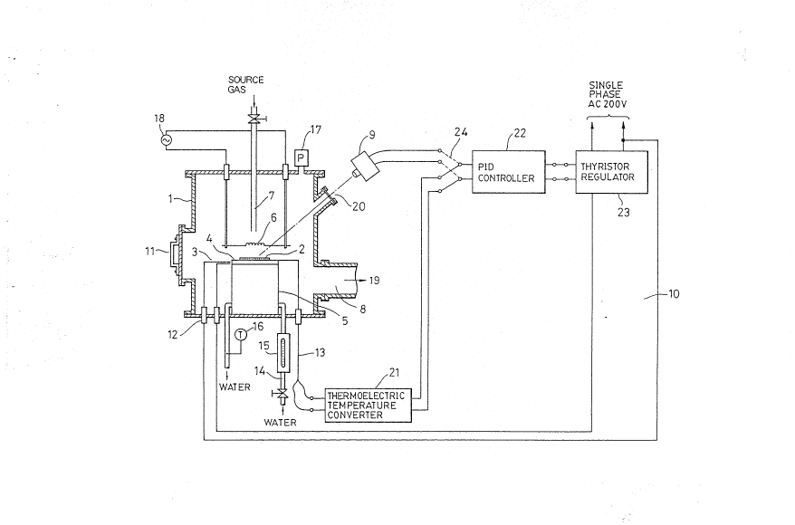
The apparatus has a reaction vessel 1 provided with a
pressure gauge 17. The reaction vessel 1 accommodates a
substrate supporting de~ice 3 for supporting a substrate 2
on which a thin film is to be formed by deposition. The
reaction vessel 1 also is provided with a work port 11
through which the substrate 2 is brought into and out of the
reaction vessel 1. The substrate supporting device 3
includes heating means 4 for heating the substrate 2 and a
cooling means 5 under the heating means 4.
2~$~
The heating means 4 includes a thermocouple 13 and is
capable of heating the substrate 2 when supplied with
electric power through power terminals 12, while the cooling
means 5 includes a cooling pipe 14 for circulating cooling
05 water~ a flowmeter 15 and a thermometer 16 for cooling
water.
The reaction vessel 1 also is provided at its upper or
lower portions with a source gas supply port 7 and a gas
exhaust port 8. A source gas such as CH4 gas diluted with
H2 gas is introduced into the reaction vessel 1 through the
source gas supply port 7 and is subjected to decompose and
the resultant gas is exhausted through the exhaust port 8 by
means of a vacuum pump 19. In order to thermally decompose
the source gas, a hot filament 6 is disposed in the reaction
vessel 1 which filament is connected to a power supply 18.
In this case, a plasma may be used in place of the
filament, as the decomposing means for decomposin~ the
source gas.
It is possible to provide a non-contact type
thermometer 9, e.g., a radiation pyrometer~ outside the
reaction vessel 1 to enable measurement of the substrate
temperature through a window 20 attached to the wall of the
reaction vessel 1.
The apparatus has temperature control means 10 which
includes, for example, a thermocouple voltage converter 21,
a PID controller 22 and a thyristor regulator 23 for
controlling the electric power supplied to the substrate
heating means 4. The temperature controller 10 controls the
2~
operation of the heating means ~ in accordance with the
substrate temperature measured by the non-contact type
thermometer 9 or the thermocouple 13, thereb~ controlling
the substrate temperature in combination with the cooling
05 means 5. A switch 24 is provided for enabling change-over
between the thermocouple 13 and the non-contact thermometer
9.
The described arrangement in the apparatus of the
present invention enables a control of the substrate
temperature over a much wider temperature range than in
known apparatuses in which the substrate temperature is
controlled solely by heating or cooling. In normal
operation of this apparatus, both the electric power and the
cooling water are simultaneously supplied and the level of
the electrical current is varied in accordance with a change
in the substrate temperature, thereby maintaining the
substrate temperature at a constant level. According to
this method, the substrate temperature can be controlled
with much higher response speed and much better accuracy
than in the case where the substrate temperature is
controlled through a control of flow rate of the cooling
water. In additionr there is no risk of boiling of the
cooling water because a certain sufficient flow rate of the
cooling water is maintained.
Another embodiment of the present invention, having a
substrate supporting device 3, heating means 4 and cooling
means 5 different from those in the first embodiment, will
~ ~ ~ 3 ~ ", !~
be described with reference to Fig. 2 which is a schematic
perspective view of this embodiment.
In this embodiment, the substrate supporting device 3
for supporting a substrate 2 is a metal bar 31 on an upper
05 portion of which is provided an RF heating coil 32 as the
heating means 4, while a cooling water pipe 14 as the
cooling means 5 is provided on a lower portion of the metal
bar 31 by silver brazing.
As a result of a study described below, the present
inventors also have considered an arrangement in which a
substrate is held by a power supply holder which also serves
as electrodes, the holder holding the substrate being placed
in a reaction vessel of a reduced pressure so that an
electric current is supplied throuyh the power supply holder
so as to heat the substrate.
Namely, the inventors prepared test pieces of silicon
substrates 50 mm long and 10 mm wide. The inventors
connected electrodes to both ends of the test piece and
supplied electric current to the test piece through these
electrodes. The test piece was not red-heated at all when
the voltage applied is still low. However, when the voltage
applied was raised to 100 V, the substrate test piece was
suddenly red-heated while drastically reducing its
resistance from several kQ to several Q or below. It was
confirmed through a measurement by a radiation pyrometer
that the substrate surface temperature can be raised up to
1300C by this methodO In addition, the substrate test
piece was uniformly red-heated over the entire portion
~3~ 'J~q~
thereof and enabled accurate measurement of the surface
temperature. It was also confirmed that the temperature
control can be done in a stable manner because the power
supply holder, which will be detailed later, can stably hold
oS the substrate without substantial change in the resistances
at the contacts between the holder and the substrate.
This apparatus will be described in detail with
reference to Fig. 3.
Referring to Fig. 3,the apparatus employs a hot
filament 6 for thermally decomposing the source gas. The
apparatus also has a heating electric power supply 43 for
supplying electric power which heats the substrate 2. A
power supply holder 41 includes a power supply electrode 42
and an insulating means 44 for insulating the cooling means
5 from the substrate 2 and the power supply electrodes. The
power supply holder 41 is capable of ho~ding the substrate 2
and supplying the substrate 2 with an electric current from
the heating electric power supply 43. The apparatus also
has cooling means 5 which is held in contact with the power
supply electrodes 42 through the insulating means 44.
Numeral 47 designates a nozzle made of quartz which
corresponds to the source gas supply port 7 and is capable
of introducing the source ~as into the zone near the surface
of the substrate ~. Numeral 9 denotes a radiation pyrometer
capable o~ measuring the substrate temperature in a non-
contact manner. These components, except the radiation
pyrometer, are encased in a reaction vessel as in the case
of the embodiment shown in Fig. 1. The substrate 2 is
disposed in the reaction vessel 1 such that its major
surfaces are held vertically. This, however, is not
exclusive and the power supply holder 41 and other
components may be arranged horizontally so that the major
05 surfaces of the substrate 2 extend substantially
horizontally as in Fig. 1.
The aforementioned radiation pyrometer g is disposed to
oppose the reverse side, i.e.,the side opposite to the thin
film depositing surface, of the substrate 2. The substrate
2, due to its high heat conductivity, exhibits almost the
same temperature at both of its surfaces. It is therefore
possible to accurately measure the temperature of the thin
film depositing surface of the substrate by the radiation
pyrometer 9 which senses the temperature of the sur~ace of
the substrate opposite to the depositing surface. If the
substrate temperature is measured directly by contacting a
thermocouple to the thin film depositing surface, a
measuring error may be caused by influence of the heat
radiated from the ~ilament 6. Such an error, however, can
be eliminated and a high accuracy of the temperature
measurement is attained since the temperature is sensed and
measured by the radiation pyrometer 9 which faces the
reverse side of the substrate 2.
In order to ensure an electrical insulation, the
insulating means 44 are interposed between the cooling means
5 such as copper chill blocks and the power supply
electrodes 42. More specifically, the arrangement is such
that substrate 2 is received in slits 46 formed in the power
12
2~3~
supply electrodes 42 and pressing screws 45 are tightened to
fix the substrate 2 between the power supply electrodes 42
and the insulating means 44. The insulating means 44 may be
formed of an insulating material such as aluminum nitride
05 plate. Although a quartz plate 2 can be used as the
material of the insulating means 44, the use of aluminum
nitride is preferred because this material exhibits a
greater insulation and higher thermal conductivity than
quartz. If the cooling means 5 is made of an insulating
; 10 material or if the surface of the cooling means 5 is
insulated, it is not necessary to interpose insulating means
between the cooling means 5 and the electrodes 42.
In view of large electrical currents supplied through
the power supply electrodes 42, each power supply electrode
42 has a large cross-sectional area so as to reduce
electrical resistance therethrough and is constructed to
tightly contact with a large surfac~e area of the substrate 2
so as to reduce the electrical and heat resistance across
the ontact between the power supply electrode 42 and the
substrate 2.
Fig.4 is a perspective view of another example of the
power supply holder.
The power supply holder employs a cooling means 5
through which cooling water is circulated. The substrate 2
is placed on the cooling means 5 such that the whole area of
one surface of the substrate 2 contacts the cooling means 5.
A pair of electrodes 42 are positioned in contact with two
spaced portions of the upper surface of the substrate 2 so
13
'
2 ~ ,
that the substrate 2 can be supplied with electric power
through these electrodes 42 from a heating electric power
supply ~3~ Thus, the substrate 2 itself functions as the
heating means by electrically heating with electric power
05 supplied thereto. When the cooling means 5 is made of an
electrically conductive material such as copper, it is
necessary that an insulating means ~4 is placed between the
substrate 2 and the cooling means 5 as illustrated.
Example l
Diamond was deposited by hot filament CYD method, using
the apparatus of the invention shown in Fig. l. In order to
attain a large density of diamond nucleation, a silicon
plate of lO mm wide, 20 mm long and 0.5 mm thickf was ground
by diamond grains of particle size of about 20 ~um, and used
as the substrate 2. A tungsten filament 6 was set at a
position about 2 mm apart from the deposition surface. At
the same time, a source gas supply nozzle for supplying a
source gas, which is a mixture of methane and hydrogen, was
set such that the end of the nozzle is about 5 mm spaced
apart from the deposition surface. The temperature of the
filament during deposition was measured by an optical
pyrometer,while the substrate temperature was measured by a
sheet-type thermocouple of 0.07 mm thick.
During the deposition, the power supply to the
substrate 2 was adjusted so as to maintain the substrate
temperature at any desired temperature between 500 and
1200C. The temperature control could be done with a very
small error of less than ~ 0.5OC. The deposition was
2 ~
conducted under the conditions of: a methane flow rate of 5
sccm, hydrogen flow rate of 50~ sccm, atmospheric pressure
of 30 Torr, filament temperature of 2100C and substrate
temperature of 850C.
05 Deposition of diamond ~ilm was confirmed by an
observation throuyh a scanning electron microscope and by
Raman spectral analysis. A section of the film was observed
by the scanning electron microscope for the measurement of
the film thickness. The film growth rate was calculated
from the film thickness to be 10 ~m/hr. ~ micro-Raman
spectral analysis was conducted on a plurality of points on
a section of the film o~ 23 ~m thick, for the measurement of
the peak intensity Id exhibited by diamond and peak
intensity Ind exhibited by non-diamond carbon. All these
measuring points exhibited the same value of the ratio
Ind/Id. The cooling was conducted by circulating cooling
water of 25C at a flow rate of 3 ~/min.
Example 2
A description will be given of the result of a test in
which diamond was formed on the substrate by CVD p~ocess
employing a co~bination of the apparatus shown in Fig. 1 and
the power supply holder of the type shown in Fig. 3. The
CVD proces was carried out by using, as the source gasl CH4
gas diluted with hydrogen gas to 1~ concentration. The
source gas was supplied from the nozzle at a rate of 2~0
sccm onto the substrate 2 placed in the reaction vessel 1 in
which an atmosphere of 30 Torr or lower pressure was
maintained. The command substrate temperature was 870C. A
2 ~ 'f~1 ~
silicon plate of lO mm wide, 20 mm long and 0.5 mm thick was
used as the substrate. In this example, the temperature of
the substrate surface could be controlled with a very small
error of ~ 0. 20C with respect to the command temperature of
05 870OC, by virtue of the heating of the substrate with
electrical current supplied to the substrate itself.
The diamond film formed by this process exhibited a
resistivity of 1013 to 1014 Qm and a hardness Hv of 8000 to
90G0 which well approximate those of natural diamonds, over
the entire area of the film.
From the foregoing description, it will be understood
that the apparatus of the present invention makes it
possible to form a thin film of uniform thickness and
quality.
Although the invention has been described through its
specific forms, it is to be understood that the described
embodiments are not exclusive. For instance, although hot
filament CVD method is used in the first and second
embodiments, the apparatus of the present invention can
equally be applied to other CVD processes such as plasma-
assisted CVD and to PVD (physical vapor deposition)
processes such as sputtering P~D, and thin films of superior
quaIity can be obtained also in such applications.
16