Note: Descriptions are shown in the official language in which they were submitted.
2 ~
[OT-972]
Description
CAPACITIV~ 8EN8IN~, 80 ~D 8TATB~TOUC~ BUTTON 8Y8T~M
Technical Fiel~
5The present invention relates to touch buttons
typically used to activate or deactivate or otherwise
control some electrical or electronic function, such as
signaling, when touched typically by a human operator
touching or "pushing" on the button with a finger. The
invention more particularly relates to a solid state
touch button system with no moving parts operated by
capacitive sensing, which can be used in many different
applications, including, for example, as a touch or push
button for elevator car calling or control.
~ackground Art
There is a need for a reliable button that does
not use or need moving parts or mechanical contacts, to
be used in, for example, elevator applications. It is
desirable that such a button be aesthetically pleasing in
appearance and use, highly reliable, low in cost and not
be activated by extreme environmental changes.
It is known that the human body has some amount
o~ capacitance to ground. A basic, previously known
concept or approach i8 to monitor a button face for
capacitance to ground, and, if a certain amount (or
greater) capacitance is present, to activate the button.
In the present invention, this monitoring of the
button surface is accomplished by monitoring the phase
shift of a signal applied to the face of the button.
30However, due to the residual impedance of the
button and the presence of external influences, the
steady state phase shift of the button can fluctuate.
Such external influences include, for example, tempera-
ture changes, cleaner residue build-up and other deposits
,
- ~ ~ 2 ~
or extreme environmental changes, etc. This fluctuation
has the potential to falsely activate a button~ which is
based on the monitoring of phase shift, although in fact
no human operator is touching the button.
A distinguishing characteristic of such exemplary
fluctuation is that it would occur slowly over a period
of time relative to a phase shift induced by the presence
of a person. To avoid this problem, in a first "auto-
balancing" embodiment of the invention the steady state
phase shift fluctuation is compensated for by 810wly auto
balancing to all phase shifts. The rate of auto balance
is set to be faster than the rate of change of the steady
state phase shift. The rate of change of phase shifts
induced by a person is faster than the auto balance rate,
which allows the button to be operated. In a second,
"constant pressure" embodiment, another way to compensate
for the exemplary fluctuations is to simply set a
threshold for activation higher than any normal fluctua-
tions.
A second potential source of false activation~ of
such a button are phase shifts induced by transient
noise. These potential transients include, for example,
electromagnetic interference (EMI) and radio frequency
interference (RFI).
A distinguishing characteristic used in the
invention to help prevent false activations caused by
transient noise is that such noise would not last for a
long period of time relative to the interaction time with
a person. Activations due to transient noise thus are
avoided in the invention by delaying the activation of
the button for a certain minimum period of time.
Di~clo9ure o~ Invention
Thus the present invention is directed to a
reliable button that does not need, and preferably does
,' , ~ '-
. . '
. : : , '. ;
:'~ .' . ' '
2~2~
not use, any moving parts or mechanical contacts and can
be used in, for example, elevator applications.
Additionally, the present invention i8 directed
to a button that is aesthetically plea~ing in appearance
and use, highly reliable, is low in cost and is not acti-
vated by extreme environmental changes.
Finally and most importantly, the present inven-
tion is directed to a phase shift monitoring, capacitive
sensing button that avoids false activation of the button
by residual impedance and external influences, such as
temperature change, cleaner residue build-up and other
deposits. The "auto-balancing" embodiment of the
invention achieves this by compensating for them by
slowly auto balancing to all such phase shifts, with the
rate of auto balance being set to be faster than the rate
of change of the steady state phase shift; while the
"constant pressure" embodiment achieves it by compensat-
ing for the exemplary fluctuations by simply setting a
threshold for activation higher than any normal fluctua-
tions. Additionally, the present invention avoids ~alseactivations by nolse transients, including those due to
EMI and RFI by delaying the activation of the button, and
the associated operative signal that causes it to be
activated, by an appropriate amount of time, such as, for
example, a time period of the order of about one hundred
(100 msec.) milliseconds.
In the exemplary "auto balancing" embodiment,
three integrators are used to provide the auto balancing
feature o~ the invention. A "medium" speed lntegrator
provides a "trigger" signal, while relatively "slow" and
"fast" integrators provide "set" and "reset" thresholds.
In accordance with another aspect o~ the inven-
tion, the purpose of the delay on the timer is for
erroneous signal re~ection, as generally mentioned above.
The erroneous signals of primary concern are those which
could be caused by extreme environmental changes.
' ~:
.
.
.: :
.
~2~
Testing has shown that any set pulses caused by exem-
plary, extreme environmental changes typically do not
last longer than one hundred (100 msec.) millisecond~
with an input resistance of, ~or example, one (l Mn)
megohms.
Further testing with the input resistor set to,
for example, two hundred and æixt~-one (261 kn) kilo-ohms
resulted without any set pulses caused by extreme
environmental conditions. From these results a delay
"on" time of the order of about one hundred (loO)
milliseconds is deemed to be appropriate.
In the exemplary "auto balance" embodiment the
delay time is achieved by a set pulse charging a capaci-
tor through resistors and a diode to a thre~hold set by
other resistors. The voltage across the charging capaci-
tor will reach the threshold, ~f a set pulse or series of
set pulses transpire without the occurrence of any
"reset" pulses.
once the threshold is reached, the output of a
comparator is released from common. The voltage on the
charging capacitor is pulled up and held high by a
hysteresis resistor, pending the occurrence of a "reset"
pulse.
At any time the voltage across the charging
capacitor can be quickly discharged by a "reset" pulse.
~ho volt~ge Aaro~ the ahArging capaaitor is discharged
through a current llmiting resistor, which resets the
timer.
Bene~its o~ the invention include the facts that
the button is:
heat resistant;
EMI resistant;
RFI re~i~tant;
ESD resistant; and
is capable of providing light and/or other feedback.
. ' ' ' .: ...... :
:.
. ..
2 ~
--5--
The invention may be pr~cticed in a wide variety
of applications, including but not restricted to,
elevator car call or control buttons, utilizing known
technology, in the light of the teachings of the inven-
tion, which are discussed in detail hereafter.
Other ~eatures and advantages will be apparentfrom the specification and claims and from the accompany-
ing drawings, which illustrate two exemplary embodiments
of the invention, an auto-balancing embodiment and a
constant pressure embodiment.
Brlof Desoription of ~raw~ng~
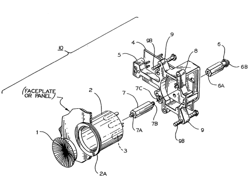
Figure 1 is an exploded, perspective view of an
exemplary solid state push button, including the button,
light ring, printed circuit (PC) board and holder ~or
attaching the PC board to the push button elements and
the overall button assembly to a face plate or panel,
with the PC board carrying the electrical components
which ~orm the exemplary electronics and circuitry of the
present invention. (It is noted that the touch button
elements of Pigur- 1 are basically symmetrical about
their longitudinal center-line, except for the PC board
and its associated holder.)
Figuros 2A & 2B are interconnected schematic
diagrams o~ an exemplary circuit for the button system of
the present invention with auto balancing characteris-
tics, with the two schematics being connected in the
"Delay On Timer" block at the "SET/RESET" line; while
Flgures 3a & 3~ are interconnected schematic
diagrams o~ an alternate, exemplary circuit ~or the
button system of the present invention with constant
pressure characteristics, with the two schematics being
connected in the "Delay~Dwell Timer" block at the "SET"
line.
2~23~c3~
ost ~es ~or C~rry~n~ U~_~he In~t~lon
-- ~UTTON A8~MBLY ~10 )
As can be seen in F~gure 1, the exemplary "solid
state button" (SSB) 10 of the present invention prefera-
bly includes a non-moving, capacitive sensing button
surface 1, that can be used, for example, as a call
button in the car operating panel (COP) and/or hall
fixtures of an elevator system. The SSB is capable of
capacitively sensing a human touch, preferably providing
lo both visual feed back (illumination) to the button
pusher, as well as communication to the operational
control of the elevator system through, for example, a
remote station interface that the button has been
actuated, so that the system accordingly can react.
The exemplary button o~ Figure 1 includes the
non-moving button element 1 fitted within a light ring
element 2, in which ring i9 carried a circular array of
light emitting diodes (LEDs) 3 at its bottom. A printed
circuit board ~, into which the light ring element 2 is
pin inserted, is carried on the back side of the button
elements 1, 2, and is held to the button elements by a
bracket S and rear bolt 6.
The interconnecting bolt or stem 7 has a front,
threaded, male end 7A, which is screwed into the back
side of the button surfaca 1, and a rear, threaded, male
end 7B, which is screwed into the ~ront end 6A of the
rear bolt 6 with a lock washer 7C. The interconnecting
bolt 7 extends through a center, circular opening
~unseen) in the light ring element 2 and through an
opening in the PC board ~, while the head 6B of the rear
bolt 6 fits into a notch in a "U" shaped rear strap 8,
which i9 part of the bracket holder 5. When assembled,
the intermediate elements of the button assembly 10 are
held in compression between the button surface 1 and the
head 6B of the bolt 6.
-. ... .
'
2 ~
The bracket 5 includes a series of peripherally
spaced, lateral extensions 9 through which screw pins 9B
are placed for fastening the button assembly 10 to a face
plate or panel. When so fastened, the only elements of
the button assembly 10 which are seen by the user is the
non-moving, circular button surface 1 surrounded by the
translucent ring 2A, which is illuminated up by the
internally contained LEDs when the button is actuated.
The printed circuit board 4 carries on it the
electronic components and circuitry which perform the
SSB monitoring functions of the present invention.
There are two basic exemplary embodiment~ of the
present invention, a pure "constant pressure" solid
state button (CPSSB) embodiment, schematically illus-
trated in detail in Figures 3A & 3B, and a relatedpredecessor embodiment, the "auto balancing" solid state
button (ABSSB), schematically illustrated in detail in
Flgur~8 2A & 2B.
The primary difference between the "constant
pressure" solid state button (CPSSB) and the "auto
balancing" solid state button (ABSSB) is that the ABSSB
has an auto balancing feature. As generally noted above,
the purpose of the auto balancing feature is to automat-
ically accommodate for static changes in components,
packaging and the environment, while maintaining a
relatlvely high sensitivity to sensing when the button
aetually has been aetuated. Due to the basic operation
of auto balancing, the ABSSB is not a pure, "eonstant
pressure" type button and, in the exemplary appliaation
of an elevator system, iB not applied to, for example,
"door open," "door close" and other applications requir-
ing a pure constant pressure (CP) feature. In contrast
the CPSSB module can be used, if desired, for all
applications in the elevator system except the alarm
button, which has special requirements.
. .
.. . .
-- 2~2~ 3~
- T~EORY OF OP~ATION -
If a button touch is constantly maintained ~or,
for example, one hundred (100 msec.) milliseconds, the
button module 10 will turn "on" its output and illumina-
tion long enough to be read and controlled by theoperational control system without loss of the call or
illumination. The illumination input preferably is
controlled by the operational control system.
The ABSSB is reset upon the removal of the
illumination control input. The illumination control of
the CPSS8 can also be used as an output when applied to
other systems.
- CIRCUI~ DE8CRIPTION -
The basic functions for each embodiment (CPSSB &
ABSSB) are as follows:
Auto-Balance ~ABSSB) Constant Pressure
(CPSSB)
Power Power
Oscillator Oscillator
PhaseShiftToPulseWidth PhaseShiftToPulseWidth
Converter Converter
Integrators Integrators
Set&Reset Comparators Level Detector
Electrostatic Discharge Electrostatic Discharge
(ESD) Protection (ESD) Protection
Delay on Timer Delay/Dwell Timer
Dwell on Timer
Output Control Output Control
High Out High Out
Illumination Current Illumination Current
Regulator Regulator
PowerUp & Control System
Reset Functions
Figure~ 2A & 2B and 3A & 3B are schematics o~ the
"auto balance~ embodiment and the "constant pressure~'
embodiments, respectively, with these functions outlined
in block form.
- POWER -
~he power aspects of the two embodiments repre-
sent standard approaches and their operation (and many
:. :
.;
.
2~2~8
alternatives thereto) are known to thosé of ordinary
skill.
- 08C~LLATOR -
The oscillator generates, for example, a square
wave of an appropriate cycle. The threshold voltage to
the non-inverting input of comparator Ul~ is set by
resistors R2 & R3, and the state of thè output of UlA,
which controls the hysteresis resistor R~. The "on"
state threshold is higher than the "off" state threshold.
The oscillator i8 controlled by the charging and
discharging of capacitor Cl. When comparator ~lA is in
the "on" state, capacitor C1 will charge to the "on"
state threshold, and, as a result, the comparator will
turn "off." Conversely, when comparator UlA is in the
"off" state, capacitor Cl will discharge to the "off"
state threshold, and, as a result, the comparator will
turn "on."
This is standard oscillator circuitry, and its
operation and various alternatives are known to those of
ordinary skill.
- P~A8E ~HIFT TO PUL~E WIDTH CONVERTER -
** Auto B~l~nce 88B **
The phase shift to pulse width converter func-
tions as follows. The oscillator is fed directly into
the non-inverting input of UlC. When the oscillator is
high, the output of UlC is released, providing the rising
edge of the pulse. The inverting input of UlB monitors
the phase shift o~ the oscillator through resistor R7
across the button input impedance. (The factors which
contribute to the button input impedance are the capaci-
tor C3, the ESD protection circuit and what is applied to
or acquired by the button face.)
When the voltage at the inverting input of U~B
reaches the threshold voltage on the non-inverting input,
the output of UlB is pulled to common, at the falling
edge of the pulse.
-- ` 2 ~ ~ ~ f c~ ~
--10--
There is always a pulse, even without anything
applied to the button face 1. The pulse is due to the
impedance of capacitor C3, the ESD protection circuit and
any residuals in the circuit.
Capacitor c3 is u~ed to prevent any DC voltage
from being placed on the button face. The value of the
capacitor C3 should be significantly larger than the
capacitive sensitivity to be obtained.
The larger the value of the resistor R7, the
larger the phase shift is for a given input impedance,
including the effects of resistance and noise. The value
of the resistor R7 preferably is chosen to generate as
large a phase shift as possible from the input.
** Constant Pres~ure 88B **
Functions on the CPSSB preferably are combined
and condensed to reduce the number of required compo-
nents. The function of UlC, R~5, and R46 in the "Phase
Shift To Pulse Width Converter" block of the ABSSB can be
condensed by, for example, replacing them with the diode
CR2 on the CPSSB for its "Phase Shift To Pulse Width
Converter" block. The functional performance of the
pulse width to phase shift converter remains the same.
- INTEGRATOR8 -
The integrators convert the pulse into a DC
voltage. The DC voltage i8 equal to the duty cycle of
the pulse multiplied by "Vcc," the regulated supply
voltage.
** Auto Balance 8~ **
The pulse from the "phase shift to pulse width
converter" is fed into three different R-C integrators.
Each integrator has a different time constant, providing
relatively "slow" ~R13 x C~), "medium" (R14//R16 x C5)
and "fast" (R15 x C6) time constants. The "medium"
integrator has a resistor (R16) in parallel with its
capacitor to act as a voltage divider. The voltage
divider insures that the steady state DC voltage of the
21~2~ $
--11--
"medium" integrator will be less than that of the "slow"
and "fast lntegrators.
The three integrators of Figure 2A provide the
auto balancing feature of the invention. The "medium"
S speed integrator provides the "trigger" signal, while the
"slow" and "fast" integrators provide the "set" and
"reset" thresholds.
The selection criteria for the integrator time
constants is given below.
** Constant Pres~ure ~8~ **
In contrast, since the deletion of the auto
balance feature is part of the purpose of the CPSSB, only
one integrator is required for the CPSSB (F~g. 3A).
- 8ET AND RE8ET COMPARATOR8 AND ~VEL DETECTOR8 -
- 15 ** Auto Balanco 8~B 8et an~ Reset Comparators **
The purpose of the set comparator (U2A) is to
provide a set pulse resulting from an increase in the
pulse width from the "phase shift to pulse width conver-
ter." A set pulse is defined as a continuous release,
from common, of the set comparator's output for any
duration of time. The set comparator will release its
open collector output, whenever the DC level of the
"medium" integrator is greater than the DC level of the
"slow" integrator.
The purpose o~ the reset comparator (U2B) is to
provide a "reset" pulse resulting from a decrease in the
"phase shift of the pulse width converter's" pulse width.
A "reset" pulse is de~ined as a continuou3 pull to common
of the reset comparator's output for any duration. The
reset comparator will pull its open collector output to
common, whenever the DC level of the "fast" integrator is
less than the DC level of the "medium" integrator.
The "slow" integrator time preferably is set as
slow as required, in order to maintain the required time
constant differences between the integrators and minimize
the ripple voltage of the "fast" integrator.
--- 2~2~'3~
The "medium" integrator time constant and voltage
divider preferably is chosen to obtain a "set" pulse with
a duration equal to the delay "on" time.
The "fast" integrator's time constant preferably
is chosen to obtain a "recet" pulse upon the removal of
a minimal input. A minimal input is defined as the
smallest amount of impedance which could cause a set
pulse.
Exemplary values for the "Integrators" block is
set out below:
Component Valyç
Rl3 200Kn
Rl~ looKn
R15 looKn
C4 l~F
C5 0.68~F
CC 0.047~F
** Constant Pressure 88B Level Deteotor **
The purpose of the level detector i8 to activate
the button as long as the voltage on the integrator
exceeds the fixed threshold. The integrator voltage
being compared to a fixed threshold is what makes this a
constant pressure ~CP) device.
Several factors contribute to the setting of the
threshold set by the resistors R13 and R14. The thresh-
old is set to allow for component tolerance variations
within the specified working temperature range. The
sensitivity of the button set by the threshold may be
set to, for example, forty (40 pF) picofarads with
nominal component values and should be no less than the
pro~ected "worst case" scenario.
- ELECTRO8TATIC DI8CHARGB ~E8D) PROTECTION -
The primary part of the electrostatic discharge
(ESD) protection circuit is the spark gap 8Gl. In the
event of an ESD the spark gap will activate and provide
a low impedance path to earth via connector J4-l.
Connector J4-1 preferably is connected to the
face plate of the button with a short wire. In hall
.
' : ~' -'',
,
- ~23~lC~
-13-
fixture applications the face plate should be connected
to the masonry box with, for example, an insulated flat
braided conductor. The masonry box in turn should be
bonded to building steel through wiring conduit or a flat
braided conductor to the closest building steel.
The spark gap is a relatively slow device, and,
therefore, the zener diode CRl is used to limit any
incoming voltage to, for example, thirty volts (30V).
The purpose of resistor Rl is to limit the current
through the zener diode CR~ and absorb the major portion
of the energy.
Resistor Rl may be selected to be of carbon
composition due to their pulse energy handling capability
and size. On the auto balance SSB the printed circuit
(PC) board is conformably coated to prevent uncontrolled
arching on the PC board during an ESD.
On the constant pressure SSB connector J4 may be
a separate connector from Jl to maintain, for example, a
quarter inch (0.25") spacing between the chassis ground
and the rest of the circuit. The relatively large
spacing is required to prevent uncontrolled arcing on the
PC board during an ESD. During an ESD the potential of
J4 will rise due to the very high frequency components of
the ESD and the inductance of the chassis ground lead.
Appropriate spacing is also required ~rom the
button connection to the button face. The electrical
connectlon to the button face can be achieved with, for
example, approprlate wlre soldered into the PC board and
a ring terminal to the intermediate button stem or
interconnecting bolt 7 (note F~g. 1), which bolt holds
and electrically connects the button face and the PC
board.
- AUTO BAL~NCE 88B DE~AY ON TIME~ -
In accordance with the invention the purpose of
the delay on the timer is for erroneous signal rejection.
As generally discussed above, the erroneous signals of
2~2~
primary concern are those which could be caused by heat
or other like eXtremQ environmental changes. Testing has
shown that any set pulse~ caused by extreme environmental
changes typically do not last longer than one hundred
(100 msec.) milliseconds with an input resistance (R7)
of, for example, one (1 Mn) megohms.
Further testing with the resistor R7 set to, for
example, two hundred and sixty-one (261 kn) kilo-ohms
resulted without any set pulses caused by extreme
environmenta change. From these results a delay "on"
time of, for example, one hundred (100) milliseconds is
deemed to be more than adequate for exemplary purposes.
The delay time may be achieved by a set pulse
charging capacitor C8 through resistors R17, R18 and
diode CR2 to a threshold set by resistors R20 and R21.
The voltage across capacitor C8 will reach the threshold,
if a set pulse or series of set pulses transpire without
the occurrence of any "reset" pulses.
once the threshold is reached, the output of
comparator U2C is released from common. The voltage on
capacitor C8 is pulled up and held high by hysteresis
resistor R22, pending the occurrence of a "reset" pulse.
At any time the voltage across C8 can be quickly
discharged by a "reset" pulse. The voltage across
capacitor C~ is discharged through the current limiting
resistor R19, which resets the timer.
- AUTO ~ALANCE 88~ DWE~L ON TIMER -
The purpose Or the dwell "on" tlme is to insure
that, once an input to the button face has activated the
button, a call will be registered regardless of subse-
guent changes to the input.
When the output of U2C is released from common,
the capacitor C9 is quickly charged through R23 and CR3.
Once the voltage across the capacitor C9 reaches the
"inactive" tkreshold, the output of comparator U2D is
pulled to common. When the output of U2D is pulled to
.. ~0
..
~2~ j3
-15-
common, the button i3 activated. The threshold voltage
to the non-inverting input of comparator U2D is set by
resistors R2~ & R25 and the state of the output of U2D,
which controls the hysteresis resistor R27.
The dwell "on" time begins when the input to the
button face is removed, and, as a result, the output o~
~2C is pulled to common. The voltage across the capaci-
tor C9 is discharged through resistor R26, providing the
dwell "on" time. Once the voltage across the capacitor
C9 reaches the "active" threshold, the output o~ compara-
tor U2D is released from common, deactivating the output
control.
Resistor R16 limits the discharge current to
protect the output of UlC. Resistors R17 and R16 create
a voltage divider to which capacitor C6 will discharge.
Re~istor R17 was selected to set the voltage of the
divider lower than the "active" threshold voltage.
Diode CR7 protects Q6 by limiting the emitter to
base voltage. When the output of comparator UlC is
released and comparator UlD is pulled to common, a
voltage divider is created by R17, CR7, and R19. This
voltage divlder sets the voltage on the capacitor C6,
while the button 1 is being held in the active state.
The difference between the voltage divider and the
"active" threshold level provides the "dv" or di~ference
in voltage ~or the dwell time.
Diode CR3 prevents leakage current through
transistor Q6, which would decrease the delay on time
provided by the charging o~ the capacitor C6.
- CON8TANT PRES8UR~ SSB DELAY/DWE~L TIMER -
The delay/dwell of the CPSSB timer combines the
purposes and functions o~ the ABSSB's delay and dwell
timers.
The delay "on" time is initiated upon the release
of the level detector's output from common, allowing
capacitor C6 to charge through resistor R17. Once the
2 3 ~ e,; g
-16-
voltage on C6 reaches the "inactive~' threshold the output
o~ comparator UlD i8 pulled to common, activating the
output control. The threshold voltage to the non-
inverting ~nput of comparator UlD i8 set by resistors R20
& R21 and the state o~ the output o~ u2~ which controla
the hysteresis resistor R22. The time required to charge
C6 provides the delay "on" time.
If the input tot he button face is removed prior
to the output of nlD being pulled to common the delay
"on" time will be quickly reset. As a result of the
input to the button face being removed the output of UlC
is pulled to common, providing a discharge path for C6
via CR3, Q6 and R16. Since the output of UlD is not
pulled to sommon, transistor Q6 will be active during the
discharge of capacitor C6. The activation of transistor
Q6 effectively removes resistor R18 from the discharge
path of C6, allowing the delay "on" time to be quickly
reset.
The dwell "on" time begins when the input to the
button face is removed after the output of UlD is pulled
to common. ~he voltage across capacitor C6 i8 discharged
through resistors R16 and R18, providing the dwell "on"
time. Once the voltage across C6 reaches the "active"
threshold the output of comparator U2D is released from
common, deactivating the output control.
Resistor Rl6 limits the discharge current to
protect the output of UlC. Resistors R17 & R16 create a
voltage divider to which the capacitor C6 will discharge.
Re~i~tor R17 was selected to set the voltage of the
divider lower than the "active" threshold voltage.
Diode CR7 protects transistor Q6 by limiting the
emitter-to-base voltage. When the output of UlC is
released and UlD is pulled to common, a voltage divider
is created by resistor R17, diode CR7 and resistor Rl9.
This voltage divider sets the voltage on capacitor C6,
while the button is being held in the active state. The
2~2~
difference between the voltage divider and the "actlve"
threshold level provides the "dv" for the dwell time.
Diode CR3 prevents leakage current through QC,
which would decrease the delay "on" time provided by the
charging of capacitor C6.
- O~TPUT CONTROL -
The output control provides the active pull to
common required by the "high out" and "illumination
current regulator" functions.
Transistor Ql of the output control provides the
signal inversion required between the output of compara-
tor U2~ and the output driving transistor Q2.
Transistor Q2 was chosen to have the current
rating required to drive the "high out" and "illumina-
tion current regulator" functions.- HIGH OUT -
The button assembly 10 is designed to interfaceto a remote station module in an elevator system. The
output to the module is required to be an aative high
level. The high level is provided through resistor R~0,
when the transistor Q3 is driven into saturation by
transistor Q2, pulling resistor R39 to common.
Resistor R40 is a current limiting resistor,
which protects the transistor Q3 in the case of an
accidental shorting of the output to ground.
- ILLUMINATION CURRENT R~CULATOR -
The illumination i9 controlled by the button 1
through transistor Q2 or the module through connector
Jl-2. The illumination is comprised, for example, of two
external strings of LEDs being fed by dedicated current
regulators through connectors J2 and J3. The current
through each string is regulated to, for example, thirty
(30mA) milliamps, by controlling the voltage across the
resistors R~2 and R~3 with zener diode CR7.
The value of resistor R41 was selected to provide
the proper current dependent voltage across diode CR7.
'~ - .
2 1~ 2 ~
-18-
The signal diode CRB is used to isolate the high
level output ~rom the illumination control o~ the remote
station module. This isolation allows the operational
controller to be signaled, when the button i8 releaged.
Due to the minimum input voltage requirement of,
for example, twenty and four-tenths volts DC (20.4 VDC)
the nine light ring LEDs were divided into two strings.
- POWER UP AND CONTROL ~Y8TEM ~B~T PUNCTION8 -
The power up reset insures that the button does
not activate due to power outages of arbitrary duration.
Upon the application of power, capacitor C10 will charge
at a rate set by the resistors R31 and R32 to a threshold
set by resistors R33 and R3~. The output of comparator
UlD is pulled to common, while the capacitor C10 is
charging. The output o~ the comparator UlD being pulled
to common prevents the capacitor C8 from charging, while
the integrators charge to their steady state levels.
The purpose o~ diode CR~ is to quickly discharge
the capacitor C10 in the event o~ short power outages.
A system reset is provided due to the remote
possibility that noise could activate and latch the
button 1. Under normal operation the button 1, when
activated, will provide a high output to its remote
station.
The operational control system will read in and
acknowledge the call by turning on the appropriate remote
station output. The output will pull the 'I/ILL W." input
to common, turning "on" the illumination.
Once the elevator arrives at the ~loor, the
control system typi¢ally will check the button output to
see if a person is trying to hold the doors open with the
call button. If the button output is active, the control
system will hold the doors open and leave the button's
illumination on. In the event the button is latched
active or the person "fell asleep," the operational
control system could remove its pull to common on the
.
,
2~2~v~
"/ILL~M." input, turning the illumination "off" and
providinq a reset.
When the ~/ILLUM." input is pulled to common, the
bias across capacitor Cll is reversed. The capacitor Cll
will discharge through diodes CR5 and CR6 and current
limiting resistor R3C.
After discharging, the capacitor Cll will be
charged to a voltage set by resistors R33 and R34. When
the "/ILLUM." input pull to common is removed, the charge
across the capacitor Cll will temporarily increase the
voltage to the inverting input of comparator UlD. While
the voltage of the non-inverting input is greater than
the threshold set by resistors R31 and R32, the output of
comparator UlD will be pulled to common discharging the
capacitor C8.
Diode CR6 is used to prevent the voltage to the
non-inverting input o~ the comparator ~lD from going too
far below common, when the bias on the capacitor Cll i8
reversed.
Diode CR6 is used to prevent any current from
~lowing through resistor R35 from the "Illumination
Current Regulator" function.
Diode CR9 i8 used to isolate the reset function
from the Output Control.
- CIRCUITRY DETAIL8 -
Of course the circuits shown and described are
exemplary and sub~ect to great variation. The specific
values of each of the resistors, capacitors and diodes
are not key to the invention and many workable values of
them are available and known to those o~ ordinary skill.
The exemplary solid state button assembly de-
scribed in detail above is designed to be applied in a
hall fixture and car operating panel ~COP) of an eleva-
tor, although, of course, many other uses and applica-
tions are possible. The exemplary unit described is a
.,
,
,'" , ~ ; '
--~` 2~2~
-20-
low cost, easily replaceable device, taking, for example,
flve (5) minutes to replace.
Although this invention has been shown and
described with respect to detailed, exemplary embodiments
thereof, it should be understood by those s~illed in the
art that various changeR in form, detail, methodology
and/or approach may be madQ without departing from the
spirit and scope of this invention.
Having thus described two exemplary embodiments
of the invention, that which is new and desired to be
secured by Letters Patent is claimed below.