Note: Descriptions are shown in the official language in which they were submitted.
2~142
-- 1 --
Improvements in or relatinc~ to Balun Transformers
The present invention relates to baluns, that is
transformers capable of matching a single-ended output to a
balanced input and vice versa.
As an example of the application of a balun consider a
high power transistor amplifier. Where output power
requirements exceed that which can be delivered by a single
transistor, a plurality of transistors may be coupled to share
the power demand. In the base station of a cellular radio
network, for example, operating in the high frequency region of
900 MHz, an output power requirement at the antenna feed of 1
kwatt would be typical, delivered by ten 100 watt amplifier
modules. Presently the upper limit power capability of radio-
frequency (r . f . ) power transistors is in the region of 60 watt,
hence to provide such a lO0 watt module coupled transistors
must be used.
A convenient and useful method of coupling two transistors
is the technique known in the art as "push-pull". Here the
drive is shared between a transistor driving current through
the load in one direction and a second transistor driving
current through the load in the opposite direction. The
arrangement is advantageous in terms of impedance matching,
presenting a higher output impedance than the very low
impedance of a single transistor or the yet lower impedance of
parallel transistors, the higher output impedance being closer
to the typical target impedance of 50, but unfortunately is
inherently a balanced system, that is it produces an output
signal which is symmetrical with respect to the common ground
potential of the coupled transistors j whereas typically a
single-ended (that is ground referenced) output signal is
required. A solution to this problem is to provide a
transformer between the output of the push-pull pair and the
load. By virtue of its isolating properties, a transformer is
able to couple the balanced output to the
21~24 1 42
-- 2 --
single-ended load. Such a transformer is that referred to in
the art as a balun.
In the case of push-pull arrangement, a similar problem
exists in providing the complementary b~l~nced drive signals
required by the push-pull pair from a single-ended input signal
to the amplifier. A balun may be used to convert such an
unbalanced input to the balanced drive signals.
Many forms of balun, including transmission line forms,
are known in the art . Examples have been described by C . L .
Ruthroff in his paper "Some Broad-Band Transformers"
(Proceedings of the Institute of Radio Engineers, 1959), pages
1337-1342 .
In high frequency r. f . amplifier applications a coaxial
cable transmission line balun is typically used, for example a
quarter wavelength length of cable having its outer conductor
grounded at the single-ended side. An applied single-ended
input will then generate a balanced output between the cable
conductors at the remote end of the cable; equally a balanced
signal applied to the non-grounded side will produce a single-
ended output . The incorporation of such baluns in r . f . push-
pull amplifier circuits will be known to those skilled in the
art .
Although providing good performance, there are a number of
drawbacks associated with coaxial cable baluns. The baluns are
made by cutting coaxial cable to length and at high frequency
even small inaccuracies in length affect performance, also the
nature of the cable ,- ^nt is not susceptible to mechanised
placement and soldering. Hence the manufacturing tolerances
associated with manual assembly create performance variations
between one amplifier and another. In an attempt to overcome
this problem baluns of printed form, which give good
repeatability, have been tried. Printed circuit forms of
baluns are known (see for example U.S. patent 4,193,048 issued
to Nyhus). ~Jnfortunately, a conventional construction printed
flat on a circuit board cannot be used
2024 1 42
3 --
in high power applications due to the proximity of the large
metal heatsinks associated with the amplifying transistors.
5 Inevitably, one side of the circuit board is closer to the
metal than the other causing an unacceptable 1 `-lAnce in
parasitic capacitances applied to the balun. To date, only
simple printed forms have been used on separate boards mounted
normal to the amplifier circuit board to give parasitic
10 symmetry. Such boards are mechanically vulnerable and although
repeatable in themselves, cannot be automatically assembled.
The present invention, by contrast, provides a balun
construction, useful in high power applications which may be
printed flat.
According to the present invention there is provided a
balun providing a single-ended signal port and a balanced
signal port, the balun including:-
a plurality of serially connected first conductor elements
extending between said single-ended signal port and ground,
and a plurality of second conductor elements
transformingly coupled to the first conductor elements and
electrically isolated therefrom,
said second conductor elements extending in electrical
symmetry from ground to said balanced port.
Preferably the conductor elements take the form of a
contiguous merged conductor, which may be of similar form, such
as, for example of closed loop form. Advantageously, the
second conductor elements extend from a common ground. The
conductors may be realised in printed circuit form.
In a preferred form of the present invention suitable for
wide band applications, a leakage compensation capacitor is
connected at the balanced output port and conductor elements
may be surrounded by a grounded conductor.
A balun in accordance with the present invention may be
used in an amplifier, such as a high power r. f . amplifier
including a push-pull stage.
_ 4 2024 1 42
In order that features and advantages of the present
invention may be further appreciated embodiments will now be
5 described, by way of example only, with reference to the
ac- -nying diagrammatic drawings, of which:-
Figure 1 represents a balun in accordance with the presentlnvent ion;
Figure 2 represents a form of the balun of Figure l;
Figure 3 (a) represents a view of a printed circuit form of
balun in accordance with the present invention from one side of
a printed circuit board;
Figure 3 (b) represents opposite side;
Figure 3 (c) represents the decoupled version of Figure
3 (a);
Figure 4 represents a push-pull r. f . power amplifier
including baluns in accordance with the present invention; and
Figure 5 is a sectional view of the amplifier of Figure 4
constructed on a printed circuit board.
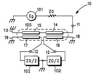
A balun 10 (Figure 1) provides a single-ended signal port
11 and a balanced signal port 12. Conductor elements 19 and 15
form a first element group extending from the single-ended port
11 to a ground 13. Conductor elements 16 and 17 extend from
the balanced port 12 to grounds 18, 19 respectively and are
electrically symmetrical. Conductor elements 14 and 15
constitute a first conductor pair which is electrically
isolated from a second conductor pair constituted by conductor
elements 16 and 17. In use, a signal applied to the single-
ended port 11 produces a balanced signal output at balanced
signal port 12 by virtue of transformer coupling (indicated
diagrammatically at 100) between the first conductor pair
(14,15) acting as a primary and the second conductor pair
(16,17) acting as a secondary. For example, a signal due to a
single-ended generator 101 may drive a balanced load 102 of
35 value ZO Alternatively, a balanced
20~41 42
signal applied to the balanced port 12 yields a single-ended
output signal at port 11. In this arrangement conductors 16,17
5 constitute the primary and conductors lg, 15 the secondary.
In a preferred form of the present invention, conductors 14
and lS are formed as a single merged conductor 20 (Figure 2) and
grounds 18 and 19 formed at a common point 21 which is a cold
point, and which can be decoupled by a capacitor 25 to connect a
power supply feed 23 (Figure 3 (c) ), so that conductors 16,17 are
also formed as a single conductor 22. Otherwise similar parts
bear the same reference numerals as in Figure 1.
It will be appreciated that this form of the present
invention lends itself to fabrication on a printed circuit board
15 construction, conductors 20 and 22 being printed directly upon
the printed circuit board surface. The resultant arrangement
may be seen more clearly in Figures 3a-3c wherein similar parts
bear common reference numerals with Figure 1 and 2. In the
arrangement of Figures 3a-3c conductor 20 on one side of the
20 printed circuit, conductor 22 on the other side and port
connections 11 and 12 are :.uLL~Jullded by a ground plane 30.
Proximity of the ground plane establishes this as the principle
source of parasitic capacitances coupled to the transformer,
hence reducing the effect of other stray capacitances which may
25 be present. The ground plane may be omitted on the upper
surface of the board, if desired.
A number of advantages of this printed form of the present
invention will now be apparent to those skilled in the art. The
balun is printed flat on the printed circuit board, which may be
30 the same printed circuit board as carries an amplifier, for
example, and so is repeatable with printed circuit board
precision. No assembly is required and there is no component or
assembly tolerance to affect circuit performance.
The embodiments of the balun described thus far are
35 suitable for use in a high frequency r.f. power amplifier
i
2024 ~ 42
-- 6 --
circuit utilising transistors in push-pull. An amplifier 40
(Figure 4, in which baluns are shown in schematic
S representation) comprises two transistors 41, 41 ' arranged in a
push-pull configuration. The actual circuit suitable in a
given application being within the competence of those skilled
in the art. An input signal for amplification may be applied
at single-ended input 45. A balun 48 in accordance with the
10 present invention provides complementary balanced signals on
lines 49,49' to drive the push-pull pair 41,41' from the
printed matching network 405, which in turn provides a balanced
amplified output on lines 400, 400 ' via a second matching
network 406 including microstrip lines, such as line 407 to be
converted to a single-ended final output at 401 by balun 402.
The baluns 48 and 402 have capacitors 403, 404 connected across
their respective balanced ports to compensate for leakages in
wide-band applications.
A constructed form 50 of the push-pull amplifier of Figure
4 (Figure 5) is mounted on a printed circuit board 51 which may
be made of teflon/glass material as suitable for r. f .
applications. Baluns 48 and 402 have conductors 20',22' and
20",22" respectively present on respective sides of the board
51. The conductors are surrounded by ground plane 30 ' . Power
transistors (41, 41 ' ) in a single package 55, has its metal
mounting plate 52 fixed to a metal heat-sink 53 by bolt 54 so
that it is connected to ground. The base and collector
transistor supplies may be connected via decoupled baluns of
the type shown in Figure 3 (c) . Heatsink 53 is required to be
massive in view of the high heat dissipation of transistor,
which typically would be operating in class AB, or even class A
both of which are relatively inefficient, hence heatsink 53
extends the length of board 51 to provide a compact structure
as is required to keep a complete high power r.f. amplifier
(consisting of many such amplifiers) of reasonable size. Cut
outs 57, 58 are provided in heatsink 53 to accommodate the
underside conductors of
2024 1 42
-- 7 --
baluns 48, 402 respectively.
It will be appreciated that the balanced side conductors
(22' for balun 48, 22" for balun 402) are each affected
uniformly by any parasitism there may be due to the proximity
of heatsink 53, that is both sides of the b~lAnc~ output
(balun 48~ or balanced input (balun 402) are equally affected.
This is the important result which allows the baluns to be
printed flat as part of the amplifier printed circuit board.
This is a departure from prior art printed balun arrangements
where the balanced side is formed part above and part below the
printed circuit board leading to unacceptably asymmetric
parasitic effects.
The foregoing embodiments of the present invention have
been described with reference to printed circuit board
construction, being a suitable way of providing conductor
elements electrically isolated by a dielectric carrier. It
will be appreciated, nonetheless, that the present invention is
applicable to all constructions providing electrically isolated
condu ct or s .