Note: Descriptions are shown in the official language in which they were submitted.
2~'3~
CIRCUIT ARRANGEMENT FOR CQNTROLLING THE LEVEL OF
ELECTRICAL SIGNALS
BACKGROUND OF_THE INVENTION
Field of the_Invention
The present invention relates to a circuit
arrangement for controlling the level of electrical
signals, and more particularly to a circuit wherein the
signals are controlled to a constant level.
Description of the Prior Art
A circuit arrangement of this type is present, in
principle, in conventional control amplifiers. The
term 'amplifier' is used generically and covers devices
that can both increase and decrease current as required
by the control. For the sake of simplicity,
'amplifier' will be used in the following text instead
of the term 'circuit arrangement'.
The use of an amplifier in the transmission of
analog and digital signals is unproblematic if a
continuous signal transmission is present. An
excessively high input signal can be processed, for
example, by an overmodulation of the amplifier.
Problems occur, however, in so-called 'burst operation'
in which signal bursts between large spaces are to be
processed. A non-continuous signal transmission of
20~4L3~
this type is present, for example, in the bidirectional
transmission of signals in a burst operation.
Satisfactory processing of such signals is not possible
with the amplifiers of the prior art. In the pr~or
art, the signals are distorted, because the bandwidth
and the dynamic range of the known amplifiers are not
sufficient to convert the bursts arriving at large
intervals into an output signal with a constant level.
This defect of the known amplifiers can lead to the
fact that no useful signal is available at the output.
In that case, the signal transmission is not possible
overall.
_UMMARY OF THE INVENTION
An object of the present invention is to provide a
circuit arrangement by means of which the level of
electrical signals can be controlled in a distoxtion-
free manner over a broad frequency range, even in the
case of greatly different levels.
This object is achieved with a circuit arrangement
formed of two series connected amplifiers. A first
amplifier containing a first variable resistor operates
at maximum amplification when a low input signal level
is received. A second amplifier comprises a series
20243~
connection of a second variable resistor and a current-
controlled voltage source with two complementary
outputs~ The outputs of the voltage source are
connected to a comparator and a controller with two
separate outputs. One of the controller outputs
transmits a control signal while the other output
simultaneously transmits a blocking signal. A first
output of the controller is connected with the first
variable resistor, while a second output of the
controller is connected to the second variable
resistor.
The circuit arrangement constructed in this manner
operates with low noise, because, in a critical region
when a low level input signal is received, maximum
amplification is always produced by the first
amplifier. It also guarantees a broadband manner of
operation with a large dynamic range. Overall,
distortion-free processing of the input signals is
ensured. All of this is achieved essentially through
the series connection of the two amplifiers, both of
which in turn are adjusted by the controller.
A weak input signal is first amplified by the
first amplifier with maximum amplification. If the
amplification is not sufficient, further control of the
signal level is taken over by the second amplifier. In
-3
202~3~
the case of a strong signal at the input, which must be
adjusted downwardly by the circuit arrangement, the
sequence is the reverse.
By means of this well-defined assignment of the
level regions to the first amplifier on the one hand
and to the second amplifier on the other hand, it is
ensured that, for one thing, the input stage receives
maximum amplification in the case of a low-input level
(good noise behavior) and, for another thing, that an
excessively high input level is reduced ~resistance to
overload~.
DESCRIPTION OF THE DRAWINGS
Figure 1 is a block diagram of the circuit
arrangement according to the invention.
Figure 2 is a schematic diagram of a subcomponent
of Figure 1.
DETAILED DESCRIPTION OF THE INVENTION
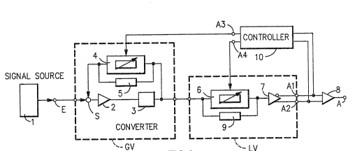
The circuit arrangement according to Figure 1
operates, for example, in the following manner:
2~2~3~
An electrical signal applied by a signal source 1
to an input E is conducted through a summation point S
to a current amplifier 2. The output current of the
current amplifier 2 is converted to an inversely
proportional voltage in a converter 3. This voltage is
conducted through a variable resistor 4 back to the
summation point S. In parallel with the variable
resistor 4 there is located an ohmic resistor 5. Both
resistors 4 and 5, together, form a feedback network.
The current amplifier 2 thus amplifies a current that
is applied to the summation point S as the difference
of the currents coming from the signal source 1 on the
one hand and from the variable resistor 4 on the other
hand. The parts 2, 3, 4 and 5 represent a first
negative feedback amplifier GV enclosed by a
dashed/dotted line, in which the feedback factor is
adjustable over a broad range greater than 40 dB.
In series with the first amplifier GV there is
located a second amplifier LV, also surrounded by a
dashed/dotted line. The amplifier LV includes a second
variable resistor 6 and a current-controlled voltage
source 7, located in series with said variable
resistor. Voltage source 7 has two complementary
outputs Al and A2. The two outputs A1 and A2 of the
voltage source 7 are connected to a comparator 8, which
2 0 ~
digitalizes the applied signal by means of amplitude
decision and makes it available as a digital signal at
the output A. In parallel with the variable resistor 6
there is located an ohmic resistor 9.
The output signal of the voltage source 7 is
symmetrically picked off at the outputs Al and A2 and
is supplied to a controller 10, which has two outputs
A3 and A4, which are inverse in a preferred
embodiment. Voltages of identical magnitude but
opposite sign are then available at these outputs. The
variable resistor 4 is acted on via the output A3,
while the output A4 controls the variable resistor 6.
The outputs A3 and A4 of the controller 10 need
not be of inverse design. It must only be ensured that
the one output supplies a blocking signal, so that the
connected resistor is not af~ected when the other
output transmits a controlling signal. This can be
achieved, for example, by the fact that the output from
which a blocking signal is transmitted is grounded.
Let us assume that the signal source 1 supplies a
strong signal, which leads to an excessively high level
at the outputs Al and A2 of the voltage source 7. The
excessively high output signal of the voltage source 7
is supplied to the controller 10, which can be, for
example, an integral controller, and which adjusts the
20~3~
variable resistor 6 via its output A4. The, for
axample, positive voltage at the output A4 is reduced
by the controller 10 for this purpose, so that the
resistance value of the resistor 6 is increased. At
the same time, the voltage at the output A3 remains
negative or grounded/ so that a blocking signal i5
transmitted from this output and the resistor 4 is not
adjusted. Overall/ the level at the outputs Al and A2
of the voltage source 7 is reduced as a result.
The reduction of this output level by the resistor
6 is limited by the parallel resistor 9~ so that the
high-spectral components of the signal are not
primarily transmitted via unavoidable series
capacitances. This would result in signal
distortions. As a result of the dynamic limitation by
means of the resistor 9, the desired decrease in the
level at the outputs A1 and A2 cannot be achieved,
under some conditions, by means of the variable
resistor 6 alone.
2Q Simultaneously with the reduction of the positive
voltage at the output A4 of the controller 10 (in the
case of inverse outputs A3 and A4), the negative
voltage at its output A3 is reduced in magnitude.
However, this is not initially sufficient to adjust the
variable resistor 4. Only when the voltage at the
~ ~2 l~ s~
output A3 becomes positive does this lead to an
adjustment of the resistor 4. The negative voltage of
the output A4 of the controller 10 maintains the
resistor 6 at the adjusted value, as a blocking signal.
If, therefore, a reduction of the level at the
outputs Al and A2 of the voltage source 7 is no longer
possibla with the resistor 6, but this level is still
too high, then the further downward adjustment is
carried out by means of the variable resistor 4. With
increasing positive voltage at the output A3 of the
controllar 10, the resistance value of the variable
resistor 4 is reduced, so that the difference in the
currents at the summation point S becomes smaller (the
effective negative feedback is then increased). The
current amplifier 2 is therefore supplied with such a
greatly reduced current that the desired stable level
is present at the outputs Al and A2 of the voltage
source 7.
If only a weak signal is supplied by the signal
source 1, the following happens:
The variable resistor 4 is first increased in
value by a decreasing positive voltage at the output A3
of the controller 10. The maximum value of the
feedback network 4/5 is limited by the resistor 5. In
order to be able to increase the total amplification
2 ~
further, the control voltage at the output A3 of the
controller 10 is reduced (A4 is correspondingly
increased) until the variable resistor 6 has declined
to a value from which the desired level is obtained at
the outputs A~ and A2 of the voltage source 7.
The variable resistors 4 and 6 are not linear
components. They are shown in Figure 1 in a simplified
manner as variable resistors. In a preferred
embodiment, the resistors 4 and 6 are designed as field-
effect transistors with their gate electrodes connected
respectively to the two outputs A3 and A4 of the
controller 10. In Figure 2, a field-effect transistor
of this type is shown as a variable resistor 4. This
involves a symmetrically constructed D-MOSFET, whose
gate electrode G is connected to the output A3 oP the
controller 10. The resistor 5, connected in parallel,
is connected to the electrode's source S and drain D.
The substrate electrode B is grounded. An identical
arrangement can be used for the resistor 6.
The current-controlled voltage source 7 is, for
example, a transimpedance amplifier with two
symmetrical outputs Al and A2 (push-pull outputs).