Note: Descriptions are shown in the official language in which they were submitted.
~A~KGROUN~OF TH~ INVENTIC)N
1. Field of the Invention
The present inveneion relates to a power distribution scheme in a
5 portable computer and, more specifically, to power management in a laptop
computer.
2. Prior Art
Power consumption in an electronic device is always a significant
concern and a power supply must be designed to adequately power the
0 device. Aside from the capability of the power supply to provide ample power
to power the corresponding device, heat dissipation, physical size, weight,
efficiency, and other related characteristics are paramount in designing or
selecting the power source. These characteristics become exceptionally
critical when the device the power suppiy is to support is a self-su~ficient
15 portable unit.
In many portable units, a self-supporting power source, such as a
battery, is used to provide the power when the unit is decoupled from its main
or external power source, such as 110 Volt ~C (ordinary house current).
Typically a battery is used to provide the independent and portable power
20 source. In some instances the battery functions as an auxiliary power source
to maintain certain critical circuits active, such as keeping the memory alive to
retain any information stored in the memory. In other instances, the battery
functions as the main power source to fully power the device. ~ :
In the area of information processing, miniaturization of processing
2s devices has permitted the portability of computing devices. One of the first
such portable processing devices was a hand held calculator, wherein the
calculator operated from a battery power source and could easily be carried
about by the user. The battery would power all of the functions of the calculator
J s~
and the user could readily transport the calculator without any attachment to anexternal power source. The batteries were either replaced or recharged. The
earliest calculators simply had an on/off state in which full power was available
during the on state and the power was completely shut off during the off state.
s Because of the volatile nature of many early semiconductor memories,
information stored in such volatile memories were lost when the calculator was
turned off. Subsequent calculators attempted to incorporate nonvolatile
memory, or in ths alternative, standby power was provide~ to such a memory
when the device was turned off, so that the memory retained whatever
information was present. More advanced schemes were devised to monitor
various functions, so that power was removed from various elements when
those elemsnts were not needed. Further, a time~out scheme was devised to
put the calculator in a stand-by mode, such as when a key was not depressed
after a certain time period, in order 10 preserve power. All of these features
were devised primarily to extend the time period that the device could operate
from its internal power source.
When the processing technology was expanded beyond a simple
calcula10r to enc~mpass personal desk top computers, additional constraints
were placed to power consumptivn ancl managemsnt control schemes. Aside
20 from the additional circuitry, additional memory devices consumed
considerable amounts of power. These memory devices inclwde s~mi-
conductor devices, such as read-only memories (ROMs) and random-access
memories (RAMs) which include volatile ancl non-volatile memories, floppy
disk drives and hard disk drives and o~her magnetic rnedia. Also, additional
25 power is required to power the display unit which typically includes a viewing
screen Various schsrnes were devised to monitor and control lhe power
distribution during on/off states.
~J g3 ~ L~ 2
However, as the personal desk top computer systems are made
portable, it is desirable to provide a computer which contains a fully containedpower source so that the computer is completely portable. These self -
sufficient computer systerns are typically referred to as laptops (because of the
5 small physical size and light weight) and are designed to operate for a certain
number of hours from its internal power source, which is typically a battery.
Although a variety of the portable calculator technology can be implemented
within such a laptop, additional constraints are placed in that the additional
circuitry, memory, viewing screen and any peripheral devices attached to the
0 system will necessarily consume additional power. In order to extend the self-sustaining time period of these laptops while keeping the battery size and
weight to a minimum, a sophisticated power management scheme is required to
provide power only to those circuits and devices which require such power
and to remove power, or at least to make a given circuit enter a low power
consumption mode, when that circuit is not needed. The management scheme
must also continually monitor the various circuits and devices in order that
power can be applied immediately to activate such circuits and devices when
needed.
The present invention provides for such a power management apparatus
20 for a laptop computer in order to extend the self-sustaining time period so that
the laptop computer can operale for an extended period of time once external
power is disconnected.
3. Prior Art Reterences
A number of prior art references are known for monitoring and controlling
25 the consumption of power to a device or to a portion of a device including a
means of providing a timeout when user interaction has not occurred for a
given time period. However, these references per~ain to the simpler calculator
technology or to portions of a computer system and fail to disclose the
~ Jr~
sophisticated power management scheme for a laptop of the present invention.
The references are: .
1. U.S. Patent No. 4,019,068, issued April 19, 1977, for Low Power Output
Disable Circuit For Random Access Memory;
2. U.S. Patent No. 4,074,351, issued February 14, 1978 ~or Variable
Function Programmed Calculator;
3. U.S. Patent No. 4,151,611, issued April 24, 1979 for Power Supply
Control System For Memory Systems;
4. U.S. Patent No. 4,293,927, issued October 6, 1981 for Power
0 Consumption Control System For Electronic Digital Data Processing Uevices;
5. U.S. Patent No. 4,279,020, issued July 14, 1981 for Power Supply
Circuit For A Data Processor;
6. U.S. Patent No. 4,381,5~2, issued April 26, 1983 ~or Standby Mode
Controller Utilizing Microprocessor;
15 7. U.S. Patent No. 4,409,665, issued October 11, 1983 for Turn-Off-
Processor Between Keystrokes;
8. U.S. Patent No. 4,611,289, issued Septernber 9, 1986 ~or Computer
Power Management System;
9. U.S. Patent No. 4,615,005, issued September 3a, 1986 for Data
20 Prooessing Apparatus With Clock Signal Control By Microinstruction For
Reduced Power Consumption And Method Therefor; and
10. U.S. Patent No. 4,712,196, issued December 8, 1987 ior Dala
Processing Apparatus.
d ~ 3
~UMMARY OF T~E INV~ITION
The present invention describes a power manager tor use in a laptop
cornputer. The laptop computer is a fully self-sufficient computer which is
5 powered by an internal battery when the compu~er is disconnected ~rom an
externa! power source. Because power conservation is paramount to sustain
the computer as long as possible from the internal battery, a power manager is
provided to monitor and control various circuit operations. Various units of thecomputer, including peripheral units, generally function equivalently to
0 well-known personal desktop computers. However, the power source to the
various devices are controlled by the power manager and a plurality of
transistor switches are used to switch the power source to the various devices.
The operalion of these switches is controlled by the power manager. ;
Additionally, various clock signals are also coupled through switches which
are controlled by the power manager so ~hat the clock signals can be
disconnected from certain units of the computer.
The power manager continually monitors various circuit functions such
that devices not in use have their power sources or clock signals disconnected
in order to deactivate devices to conserve battery power. The remcval of clock
20 signals from those units having clock control places these various units into an
inactive slate. However, because power is still applied 10 these units, various
internal states retain their current state until the clock signal is restored.
The power manager is capable of operating in one of three modes of
operation. In a first mode the computer operates in a normal active mode where
25 most of the units are active at all times and/or some of the other units are
caused to be made active when needed. A second state is a sleep state in
which the computer enters into an inactive state and the power manager
continues to monitor various circuit conditions. When a certain pr~determined
,
condition occurs, it causes the computer to awake from its sleep state. A third
s1ate is an intermediate state in which the power manager controls the
frequency of the clock signals to be decreased such that the power
consumption drops by approximately 25-30% from the normal active mode.
#..'~f~
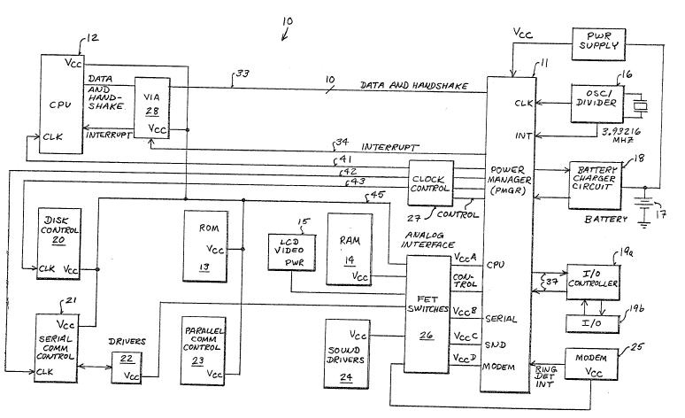
~R EF ~ESCRIPLON QF THE DRAWlN~S
Figure 1 is a circuit block diagram of the various units of the laptop
computer and showing power lines, clock signal lines and control lines
5 pertaining to the power management scherne of the present invention.
Figure 2 is a circuit schematic diagram showing an examp7e of a
transistor switch utilized to control 1he switching of a clock signal to a givendevice.
1 0 '''
Figure 3 is a circuit schematic diagram showing an example of a
transistor switch utilized to control the switching of power to a given device.
. r ~
DETAILED DE$cFllpIloN QF THE PRE~ENT I~IV~I~
A power management system for a laptop computer is described. In the
following description, numerous specific details are set forth, such as specific5 circuits, devices, etc., in order to provide a thorough understanding of the
present invention. It will be obvious, however, to one skilled in the art that the
present invention may be practiced without these specific details. In other
instances, well-known circuits and signal lines have not been described in
detail in order not to unnecessarily obscure the present invention.
0 Referring to Figure 1, an architecture ~or a portable computer 10 is
shown, including the power manager (PMGR) 11 of the present invention. -~
Although compu~er 10 can be of a variety of computers, computer 10 of the
present invention is a po~able computer and, more specifically, a laptop
computer which is capable of operating without an external power source.
Aside from the PMGR 11, computer 10 is comprised of a CPU 12, read-only
memory (ROM) 13, random-access memory (RAM) 14, liquid crystal display
(LCD) unit 15 which includes a viewing screen and associated video circuitry,
crystal controlled clock and oscillator 16, a battery 17, a battery charger circuit
18 and an input/output (I/O) unit 19 which includes an l/O controller 1 ga and at
least one l/O device 19b. These components are typically present in most
desktop or portable computer systems. Computer 10 of the present invention
further includes a disk controller 20, a serial communication controller 21 and
its drivers 22, a parallel communications controller 23, sound circuit and
drivers 24, and a modem 25. It is to ~e appreciated that although units 20-25
are included within computer 10 that these devices are typically a design
choice and the computer 10 can readily operate as a functioning ~omputer
without the presence of these units.
~ ~ 2 i~
Several additional units are included within computer 10 to operate with
the PMGR unit 11. Analog interface unit 26, clock control unit 27 and an
internal interface unit, referred to as a via unit 28, are included to function in
conjunction with the PMGR 11. IS is to be appreciated that units 12-2~ are
5 devices used in prior art computers and such description and operation of
these units are not included herein. Units 12-25, except for unit 17 and 18, areavailable with the Macintosh~' brand computers of Apple Computer Inc., of
Cupertino, California.
In functional terms, CPU 12 is the main processing unit for computer 10
10 and in the preferred embodiment is a 68000 based (part numbers 68000, 68020
and 68030) processor manu~actured by Motorola Corporation. ROM 13 is
used to store the operating system of the computer 10 as well as other
proprietary programs, such as file directory routines. RAM 14 is utilized as theinternal memory of the computer for accessing of data. The LCD display 1~
wilh its associated video circuitry provides ~or the presentation of a display sn
a viewing screen. The crystai operated clock 16 provides for the necessary
timing reference signals which are needed ~or the operation of computer 10.
The battery 17 powers computer 10, permitting computer 10 to be a fully
portable unit. Battery charger circuit 18 monitors the level of the battery 17 as
20 well as charging the battery 17 when computer 10 is coupled to an external
power source such as 110 Volts AC. `~
The l/O unit 19 interfaces with various l/O devices, such as keyboards
and cursor control devices, such as a "mouse" or a trackball. The disk
controller unit 20 is used ~o access a disk storage medium, such as a floppy
25 disk. In computer 10, a hard disk is coupled and accessed by the parallel
communications controller 23. The serial communication controller 21 and its
drivers 22 are utilized to provide serial communication, such as supporting a
RS-232 protocol. The sound circuits and drivers of sound unit 24 are utilized to
6~ f~ ! 3 ~
generate various audio signals from computer 10. Modem 25 is typically an
external device, however, in this instance it is included within computer 10 to
provide full modem capability, in order that the portable computer 10 has
capabilities of interfacing with telecommunication lines at various rernote
5 locations.
The power management apparatus of the present invention is comprised
of PMGR 11, analog interface unit 26, clock control unit 27 and via unit 28.
Functionally, PMGR 11 is an intelligent assistant to the CPU 12, wherein
PMGR 11 monitors the state of charge of battery 17, controls the power
0 consumption of the various subsystems, includes a real time clock which
frequency is determined by the clock circuit 16, interfaces to the internal
modem 25, as well as an interface to the l/O peripheral devices 1 9b through
l/O controller19a. It is to be appreciated that PMGR 11 of the preferred
embodiment includes its own ROM, RAM, timers, analog to digital converters,
15 and general purpose l/O lines. Although a variety of devices can be used to
perform the iunctions of PMGR 11, the preferred embodiment uses part number
50753, which is a semiconductor chip manufactured by Mitsubishi
Corporation.
The software stored within PMGR 11 of the present invention provides
20 for three main functions in controlling the power management of the various
devices. These functions are receiving commands from the CPU 12 and
performing in response to these commands, controlling the transfer of
communications between the PMGR and peripheral units coupled to the l/O
controller unit 19, and monitoring the system as well as providing the tim0r to
2s maintain the real ~ime clock. An 8-bit data bus and two handshake linss
provide the coupling betwesn CPU 12 and PMGR 11 through the via unit 28.
The 8-bit databus is used to transfer command and data between CPIJ 12 and
PMGR 11. This 8-bit communication is achieved by the use of a two line
tf, J ~ d
handshaking scheme wherein cornmands are provided by CPU 12 and replies
are provided by PMGR 11 on data and handshake lines 33.
Once the command is sent from CPU 12 through via unit 28 to PMGR 11
and the handshake is comple~ed, PMGR 11 decodes ~he command and
~xecutes it. If no reply data is to be returned, PMGR 11 waits for the handshakefor the next command to begin from CPU 12. If repiy data is to be returned,
PMGR 11 begins the reply handshake and returns the requested data. In the
preferred embodiment commands and replies are transmitted in a protocol
comprising of a command/reply byte, a count byte and optional data bytes.
0 Once every 1/60 of a second (frequency of 60 Hz), the clock oscillator16 generates an interrupt to PMGR 11 and this interrupt is coupled to CPU 12
on line 34. When this interrupt is generated, PMGR 11 closes the l/O channel
from l/O controller 19 and further, will not respond to any handshake requests
from CPU 12. The interrupt on line 34 causes CPU 12 to suspend the data
transferto PMGR 11. During this interrupt cycle, PMGR 11 performs its
periodic monitoring routines which include updating the real time clock,
checking the battery power level and sending an auto poll command. The auto
poll command is associated with the au~o poll scheme of the preferred
embodiment in which the CPU 12, through PMGR 11, automatically
in~errogates (polls) devices coupled to bus 37 to determine the presence of
data for transfer. .
PMGR 11 contains the necessary i/O transceiver functions for transfer of
information between PMGR 11 and l/O unit 19 on bus 37. Packets of n
information to be sent on bus 37 to l/O unit 19 are sent by CPU 12 to PMGR 11
in the data portion of the command signal. ~ata received by PMGR 11 from l/O
controller 19 is buffered internally and once received, this data is stored withln
PMGR 11 until requested by CPU 12. If a new l/O command was transmitted by
CPU 12 during a previous cornmand/execu~ion cycle, the new command and
~ ~ 7 ~ r~; c3
its corresponding data is supplied as the next l/O command which is to be sent
If the l/O device has any data ~o return, PMGR 11 receives, buffers and stores
the data. When the data is completely received, PMGR 11 interrupts CPU 12
on interrupt line 34 and CPU 12 responds to the interrupt by determining the
5 source of the interrupt and data is obtained from PMGR ~1.
PMGR 11 includes a one second timer which is based on the 60 Hz
frequency of clock 16. PMGR 11 also includes its own internai clock which
performs as a real time clock. The one second timer is used to supply a wake
up timer and create the one second interrupt for triggering the various
0 monitoring functions. That is, as each new second is counted within PMGR 11,
a number of periodic operations occur. Firstly, the real time clock and the
wake up timer (if enabled) are updated. The wake up timer is an internal alarm
clock which is used to provide an alarm/signal whenever the real time clock
coincides with the tome set for the wake up timer lif enabled). Next, computer
10's power system and battery 17 are checked to determine the battery power
ievel and if a low battery condition sxists. The battery charger circuit 18
includes means for monitoring the level of the battery and for determining if the
power level drops below a predetermined level. Then, the internal temperature
is also checked followed by the interrupt to the CPU. Subsequently PMGR 11
20 sends any pending IIO transactions to CPU 12.
It is to be appreciated that via unit 28 performs the function of an
.interface unit between the CPU 12 and PMGR 11. Via unit 28 includes general
purpose l/O devices, internal timers, interrupt generators, as well as input andoutput ports. However, it is to be noted that PMGR 11 can be readily adapted
25 to operate without such a via unit 28 without departing from the spiril and scope
of the present invention.
In order to provide the control over the consumption of power by
computer 10 for the primary purpose of extending the life of battery 17 when
~ ~3 2 '~
computer 10 is disconnected from an external power source, PMGR 11
provides for a number of control and monitoring functions for this purpose.
PMGR 11 is utilized to cause computer 10 to be in one of three separate modes
of operation. The three modss are the normal, slow and sleep modes. PMGR
5 11 responds to each of these modes by controlling the clocking signal being
sent to a given device and/or controlling the voltage being supplied to a given
unit. The clock signals coupled Irom the clock oscillator 16 to PMGR 11 are
coupled to the clock control unit 27. Clock control unit 27 operates as a switchto oouple the various clock signals on lines 41, 42 and 43 to CPU 12, serial
0 communication controller unit 21 and the disk controller unit 20, respectively.
A power supply 29, which receives its power from battery 17, provides
the needed voltag~s by computer 10. These supply voltages, shown as Vcc's
in Figure 1, are coupled through PMGR 11, wherein PMGR 11 provides
separate Vcc sources to the various units through the analog interface unit 26.
As shown in Figure 1, VccA is coupled to the CPU 12 and related units. Three
other separate Vcc sources are also provided from PMGR 11 as dedicated
Vcc voltages to serial communication drivers 22, sound unit 24 and to the -
modem 25 through analog interface unit 26. These voltages are designated as
VccB, VccC and VccD, respectively. lt is to be notecl that control lines are
20 also present between PMGR 11 and clock control unit 27 and between PMGR
11 and analog inter~ace unit 26. In the preferred embodiment, analog interface
unit 26 is comprised of a plurality of transistor switches for switching the various
Vcc sources onto their corresponding lines. The clock control unit 27 also
includes various switches for coupling the clock signals to the corresponding
25 units. Further, it is to be appreciated that PMGR 11 also includes circuitry ~or
the various clocking signals for distribution onto lines 41-43. It is to be noted
that PMGR 11 can change the various clocking rates of the clocking signals
present on lines 41-43.
13
~ ~ 2 i `` ~
In the normal (or wake) mode of operation, computer 10 is fully active
and all of the switches within clock control unit 27 and the analog inter~ace unit
26 are closed. However, commands can be provided by CPU 12 automaticaliy
in response to stored routines, or in response to a user input through l/O unit
19, to deactivate transistor switches which couple VccB, VccC and VccD, in
order to remove the applicable Vcc power from the serial communication
controller drivers 22, sound drivers of unit 24 and modem 26. Alternalively, in
order to conserve power of the battery, Vcc voltages for powering units 22, 24
and 25 need not be applied until such unit usage is requested by the system or
0 the user.
In order to further conserve power, PMGR 11 will send computer 10 into
a sleep (inactive) mode under an occurrence of either of two conditions. When
the battery charger circuit 18 notes that battery 17 has dropped to a
predetermined level, which level is deemed to be detrimental to further
lS operation of computer 10, PMGR 11 places computer 10 into a sleep mode.
PMGR 11 can also enter the sleep mode when a sleep command is provided ~;
by CPU 12. CPU sends a sleep command to PMGR 11 when there has been no
user activity for a predetermined amount of time or when the user decides to
stop work and shut down the computer 10.
Before entering the sleep mode, the operating system of the computer,
as well as the various drivers, save the current state information in RAM 14.
Thus, the state ot the various registers, drivers and other memory devices are
stored within RAM 14 for later restoration. Once these necessary states are
stored in RAM 14, PMGR 11 releases all of the switches in analog inter~ace
unit 26 so that power is removed trom the various units of computer 1û. It is tobe noted that power is removed from RAM 14 if RAM 14 is comprised of non-
volatile memory such as an EPP,OM, which is the case with the memory device
14 of the present invention. However, if RAM 14 is comprised of volatile
memory then the transistor switch applying Vcc power to RAM 14 is kept
closed so that Vcc is still applied to RAM 1~ keeping it ac~ive in order to retain
the stored information. It is to bs noted that non-volatile memory is preferred so
that Vcc need not be applied to RAM 14 in the sleep mode. Further, it is to be
5 noted that the preferred embodiment uses CMOS memory.
In an alternative embodiment, VccA can be coupled onto line 45 in
order to keep the power supplied to CPU 12. The internal clock of PMGR 11
can be decoupled from CPU 12 by clock control unit 27 thereby disabling the
clock input to CPU 12 and halting the execution of the CPU. The CPU internal
0 states are frozen with all CPU internal RAM and control registers remaining
intact by halting the execution of the CPU. Halting the execution of CPU 12
typically will lower its power consumption by two orders of magnitude.
Although a number of conditions can cause computer 10 to wake from
the sleep mode, computer 10 of the present invention has three possible
5 conditions which triggers it to leave the sleep mode. PMGR 11 continues to
monitor lines 37 such that any input from l/O controller1 9a will cause computer10 to wake from the sleep state. The l/O input is typicaliy a pressing of a key on
the keyboard and/or the movement of the cursor control device. The second
condition ~or waking up computer 10 occurs if the wake up timer (alarm clock~
20 within PMGR 11 had been enabled and matches the real time clock within
PMGR 11. Upon the activation of the alarm clock, PMGR wakes computer 10
from its sleep sta~e. Finally, the third condition of computer 10 occurs if PMGR11 was set to monitor the detection of a ring signal from modem 25. If an
incoming signal is received by modem 25, the ring signal is detected by PMGR
25 11 and causes computer 10 to awake from its sleep state.
Upon waking, computer 10 accesses RAM 14 to retrieve the stored state
of the various units for restoring computer 10 to the state it was in prior to
.3 3 r~
entering the sleep mode. Further, upon waking, computer 10 initiates a
diagnostic routine for ensuring proper operation of computer 10.
The third mode of operation of computer 10 is known as the slow rnode.
The slow mode is a condition similar to the active mode, except that the clock
5 rate of ~he clocking signal to the various units is slowed. That is, by reducing
the clock rate of computer 10, as much as 25-30% of power savings can be
obtained. Although all of the clocking signals on lines 41-43 can be slowed, it
is to be noted that the clock signal on each line can be slowed. Slowing the
clock rate of the clocking signal on line 41 to CPU 12 can achieve 25~30%
0 savings in power.
Furthermore, the slow mode is entered from the normal mode when no
activity has been detected a~er a predetermined time period, this time period
being less than the time period for placing the system into the sleep mode.
Thus, if no activity occurs for a certain duration, computer 10 enters the slow
rnode first and if the non-active cycle continues, computer 10 will eventually
enter the sleep mode after an additional time period.
The slow state can be entered and depa~ed by user command or CPU
command. It is appreciated that clock signals to units 20 and 21 can be
decoupled by clock controi unit 27, wherain units 20 and 21 are deactivated
20 and will not lose the current internal states of those units.
Referring to Figure 2, a transistor switch 50 utilized in the clock control
unit 27 is shown. It is to be apprecia~ed that only one switch 50 is shown,
however, the actual clock control unit 27 is comprised ot a plurality of these
switches 50. A clock signal from PMGR 11 is coupled through transistor 51 to
25 its corresponding device 52. The control signal is also obtained from PM(3R 11
and is coupled to the gate of the transistor 51. When transistor 51 is mad~
active by the control signal, the clock signal is coupled to device 52.
Typically, device 52 is a CMOS device so that when the clock signal is
16
removed from this CMOS device, the device shuts down and consumes none
or very little power. It is to be noted that in some of the devices, such as units
20 and 21, the clock signal can be decoupled irom thsse devices while the
Vcc supply to these devices are present.
Referring to Figure 3, a transistor switch 54 comprising one of the
switches within analog interface unit 26 is shown. However, i~ is to be noled
that a plurality of these switches reside within analog interface unit 26. One of
the Vcc lines is coupled from PMGR 11 through transistor 55 to device 56. A
control line also from PMGR 11 is coupled to the gate of transistor 55 for
0 controlling the coupling of Vcc to device 56 through transistor 55. It is to be
noted that power is supplied to device 56 when transistor 55 is rnade active
and that device 56 may not necessarily be a CMOS device since power will be
removed from device 56 when transistor 55 is cut off.
It is to be apprecia~ed that the above description in reference to Figures
1-3 can be represented in various other circuit equivalent Sorms without
departing from the spirit and scope of the invention. Further, in reference to
Figure 1, the aotual devices and the switching of the power and clock signals
can be readily adapted to operate with other designs without departing frorn thespirit and scope of the present invention. However, in order to provide a more
detailed workings of the present invention, various specific details pertaining to
the preferred embodiment are disclosed below. CPU ~2 provides various
commands to PMGR 11 for connecling the Vcc power to applicable devices as
needed. Further, clock signals can be either disconnected from varisus
devices, or in the alternative, PMGR 11 can provide different clock speeds,
such as during the slow mode. CPU 12 can be made to provide these
commands in response to a stored routine or in response to a moniloring
function of the PMGP~ or in response to a user interaction through l/O unit 19.
It is to be noted that ~he various driYers of computer 10 are responsible
for powering on and off their respective peripheral devices. It is to be notes~
that drivers of computer 10 can be hardware or software drivers, or a
combination thereot, and the preferred embodiment uses software drivers. That
5 is, software is used to control the powering on and off the respective devices.
Thus, the power to the disk control unit 20 also powers the floppy disk, ~he
power to the parallel communications controller 23 also powers its associated
peripheral device, such as the hard disk. The drivers of the serial
communications controller 21 and the power to the sound drivers 24 also are
0 controlled as needed. These drivers are responsible fsr maintaining the time
that these devices are powered to a minimum in order to conserve power.
Thus, they are only activated when a given particular device is needed.
Generally, each device driver will enable its peripheral device when the driver
is needed.
lS In the case of the floppy disk controller 20, the power is only applied tothe peripheral device when an actual disk read or write is under way. Also, in
the instance with lhe modem 25, it is kept without power until a ring is detected
by PMGR 11 or when activated by the CPU 12. As stated previously those
devices that have system clock inputs are enabled/disabled by controlling
20 their connection to the clock. They can remain powered even though the rest
of the system is off, therby retaining their internal states, but consuming lesspower. As such, clock control devices do not need be re-initialized or rs-
enabled when their clock is turned off. Those devices that do not have a clsck
input or do not require any state to be retain are enabled/disabled by
25 controlling their connection to power. As stated previously, the power can beremoved from CPU 12 in which case the internal states of CPU 12 are stored in
RAM 14 prior to power down. It is to be stressed that the clock input can be
removed from CPU 12 in which case the internal states of CPU 12 are retained.
18
a ~ i ! 3 ~
In reference to the battery charger circuit 18, the circuit charges the
battery when coupled to an external power source, but circuit 18 is also utilized
to monitor battery 17. PMGR 11 monitors the power level of battery 17 and
alerts the user when that level drops to a predetermineci level, permittin~ the
s user to finish the current job of the computer and shutting down the computer
prior to complete breakdown of computer 10. An analog-to-digital converter
within PMGR11 provides for the conversion of the analog battery voltage to a
digital signal. Although not shown in Fisure 1, a temperatura sensing
mechanism is aiso coupled to a PMGR 11 to sense the temperature and
0 another analog-to-digital converter within PMGR 11 is aiso used to convert this
analog signal to a digital signal.
It is to be appreciated that the PMGR 11 of the preferred embodiment of
the present invention provides for a variety of techniques to monitor and control
the distribution of power and clocking signals in order to conserve the time that
cornputer 10 can be self-sustaining when decoupled from an external power
source.
19