Note: Descriptions are shown in the official language in which they were submitted.
MA9-89-005 -1- 2024634
Description
SELF-POWERED SCR GATE DRIVE CIRCUIT
WITH OPTICAL ISOLATION
Background of the Invention
1. Technical Field
The invention disclosed broadly relates to power
circuits and more particularly relates to SCR power
circuits.
2. Background Art
Switching a silicon controlled rectifier (SCR) in
high power applications requires precise control of the
SCR's current to insure proper timing of the device
turn-on. Large systems operating from a power line
frequently have reactive and electronic loads that cause
distortion of the current and voltage waveforms.
Polarity reversals of the load current due to this
distortion cause undesirable mid-cycle commutation or
turn-off of the SCR.
Isolation and control of an SCR has frequently been
accomplished in the prior art with a transformer to
couple energy between the SCR gate and its controller.
Individual drive transformers required for each SCR gate
increases the complexity of this prior art driver circuit
approach. Transformer gate drivers add significant size
and weight to a design and cannot sustain a continuous DC
drive signal. The need to resupply gate signals at a
high pulse rate places severe performance limits on prior
art transformer designs for SCR drive systems.
Objects of the Invention
It is therefore an object of the invention to
provide an SCR gate drive circuit which provides precise
control of the SCR s current in order to insure proper
timing of the device turn-on.
MA9-89-005 -2- 2024634
It is a further object of the invention to provide a
self-powered SCR gate drive circuit which has a
significantly reduced size and weight.
It is yet a further object of the invention to
provide a self-powered SCR gate drive circuit which can
maintain predetermined maximum output drive current.
It is still a further object of the invention to
provide a self-powered SCR gate drive circuit which has a
high voltage isolation characteristic between the control
input and the output by means of opto-electronic
coupling.
Summary of the Invention
These and other objects, features and advantages of
the invention are accomplished by the self-powered SCR
gate drive circuit disclosed herein. The improved gate
driver circuit provides a continuous gate current
whenever there is sufficient anode-to-cathode voltage
difference across the SCR. This approach described
herein eliminates the need to monitor and reapply SCR
gate current after each commutation due to load current
distortions. Previous SCR gate driver designs used a
pulse train of gate currents to provide a means of
keeping the SCRs turned on. The pulsed gate control
approach has gaps in the SCR's operation and requires
significant circuitry that dissipates much more drive
energy.
Energy for this improved driver circuit is derived
from the SCR anode-to-cathode voltage differential. This
eliminates the need for individual power supplies to
provide isolated gate signals for each SCR. This
self-powering feature reduces the intricacy of
controlling multiple SCRs in multi-phase or unreferenced
power systems. Flexibility provided by this method
allows high power SCRs to be directly interfaced to a
digital processor-type controller.
Brief Description of the Drawings
MA9-89-005 -3- 202~634
These and other objects, features and advantages of
the invention will be more fully appreciated with
reference to the accompanying figures.
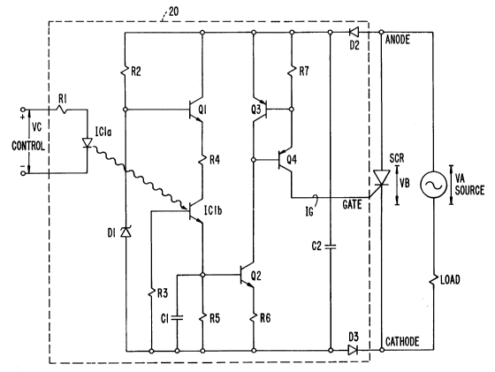
Fig. 1 is a circuit schematic diagram of the
self-powered SCR gate drive circuit invention.
Fig. 2 is a waveform diagram which shows the load
voltage waveforms for a source voltage VA, SCR
anode-to-cathode voltage VB, control voltage VC and gate
current IG.
Description of the Best Mode for Carrying Out the
Invention
The improved gate driver circuit 20 of Fig. 1,
provides a continuous gate current whenever there is
sufficient anode-to-cathode voltage difference across the
SCR. This approach described herein eliminates the need
to monitor and reapply SCR gate current after each
commutation due to load current distortions. Previous
SCR gate driver designs used a pulse train of gate
currents to provide a means of keeping the SCRs turned
on. The pulsed gate control approach has gaps in the
SCRs operation and requires significant circuitry that
dissipates much more drive energy.
Energy for this improved driver circuit 20 is
derived from the SCR anode-to-cathode voltage
differential. This eliminates the need for individual
power supplies to provide isolated gate signals for each
SCR. This self-powering feature reduces the intricacy of
controlling multiple SCRs in multi-phase or unreferenced
power systems. Flexibility provided by this method
allows high power SCRs to be directly interfaced to a
digital processor-type controller.
The anode-to-cathode voltage required to energize
this design is about four volts and is primarily governed
by the SCR gate characteristics. The gate driver circuit
consisting of transistors Ql-Q4 derives its power from
the anode and cathode terminals of the SCR. When there
is a potential difference across the anode and cathode of
the SCR, and when the control input is on at the input
transistor IClb, current will flow through the
MA9-89-005 -4- 2~2 ~ 634
transistors Ql-Q4 and there will be some power
dissipation. However, once the SCR becomes conducting,
the anode-to-cathode potential across it goes
substantially to zero volts. In this condition, since
there is substantially no potential difference across the
gate drive circuit, no current will be flowing through
transistors Q1-Q4 and there will be substantially no
power dissipation in the circuit. Alternately, when there
is no input signal applied to the base of the input
transistor IClb, and when there is a positive potential
difference across the anode and cathode terminals of the
SCR, there will be some small leakage current passing
through the transistors Ql-Q4 which will provide a very
small power dissipation. It should be noted that the
diodes D2 and D3 are polled so that when there is a
negative potential difference across the anode and
cathode terminals of the SCR, no current will be
conducted and this will prevent any reverse current
passing through the gate drive circuit. During
conduction, the SCR has a voltage drop of about two
volts, anode-to-cathode, which effectively shunts all
load energy around the driver circuit, eliminating
dissipation within the driver components.
The driver circuitry is optically isolated from the
19w voltage point signal circuitry by a photo transistor.
This technique is especially desirable in high voltage
applications and when the power system "ground" or
neutral is unreferenced. The optical isolator provides
the electrical isolation barrier between the high voltage
power circuits and the low voltage input control signal.
The SCR gate current is derived from the voltage
differential between the anode and cathode of the SCR.
The amplitude of this source voltage varies from zero to
a maximum sine wave voltage value of 175 volts in the
circuits tested. The wide variations in this source
voltage resluire control circuits to limit the drive
current impressed on the SCR gate terminal.
Gate drive is limited to provide a regulated gate
current regardless of the applied sine wave voltage
amplitude, above a minimum value of about four volts.
MA9-89-005 -5- ~24634
The current regulator Q3, Q4 and R7 in the circuit tested
was set for 80 milliamperes of gate current over an input
range of four to 175 volts. The operational description
of the entire gate driver design is given below.
In Fig. 1, the base of the output transistor Q4 is
pulled low by transistor Q2, to supply a drive signal to
the gate of the SCR. Transistor Q3, in combination with
resistor R7, limits the current through Q4 by forming a
limiter to "steal" base drive from Q4, if the current in
R7 exceeds the desired current (80 milliamperes) limit.
This assures proper gate current to the SCR, fixed in
amplitude regardless of the potential across the SCR.
Over-driving the gate of the SCR is undesirable as it
causes excessive dissipation at the gate and can lead to
failure of the SCR. Unregulated SCR gate drive places
greater stress upon the drive components and drastically
limits the operating voltage range which the design can
tolerate.
Transistor Ql and resistor R2 act as a 15 volt
regulator, limiting the internal operating voltage below
the rated voltage range of the output transistor in the
optocoupler IClb. This value is approximately equal to
the zener voltage of diode Dl; 15 volts in this circuit.
The magnitude of resistor Rl is selected so that the
input current through ICla is at an effective operating
level. When the input LED of ICIa is supplied current
from a control source, the output transistor IClb is
turned on by the photo current and conducts the 15 volt
power from Ql through a limiting resistor R4, turning on
the NPN transistor Q2. To minimize the effects of
leakage and stray photo currents, shunting resistor R5 is
added to bypass the base of Q2 and R3 bypasses IClb s
base. Cl is a timing capacitor selected to adjust the
response of the drive signal, and to filter out noise
energy picked up in the wiring of the driver circuit.
When the control signal is inactive, no photo
current is available to the output transistor of IClb and
it becomes nonconducting. Resistor R3 drains charge off
the opto transistor (IClb) base, insuring that it remains
off. This turns off Q2. With Q2 off, there is no
MA9-89-005 -6- 2 0 2 4 6 3 4
current path for Q4's base and it remains off. Q4
interrupts the flow of gate current to the SCR which
allows it to commutate naturally and switch off the power
available to the load when the anode-to-cathode voltage
on the SCR passes through zero.
Diodes D2 and D3 provide reverse polarity blocking
for the driver circuit during the period that the source
sine wave has reversed in polarity and the SCR is not
able to conduct current. C2 is a small filter capacitor
to reduce voltage spikes impressed on the driver circuit
from the noise pickup on the power control wiring and SCR
terminals.
In the circuit 20 of Fig. 1, there are two input
signal leads that are connected to ICla's LED diode and
three output leads to pick up power from and provide gate
drive to the SCR. The small physical size, low parts
count, and minimal power dissipation allow circuit 20 to
be included in the packaging of an SCR component body.
This would reduce noise, complexity and the real estate
needed to implement these SCRs in the design of new
equipment.
Fig. 2 has waveform diagrams for the source voltage
VA, the SCR anode-to-cathode voltage VB, the control
voltage VC and the gate current IG for five consecutive
periods for the source voltage waveform. In particular,
Fig. 2 illustrates the operation of the invention during
a turn-on of the control voltage at the time TA and the
turn-off of the control voltage at the time TE. During
the interval between TA and TE, it can be seen that the
gate current IG will have positive going current pulses
which provide a gate drive for the SCR. During the first
period of the source voltage sine waveform between T0 and
Tl, the control voltage VC is off and therefore the SCR
is not conducting and therefore, if there is no reactance
in the load, the SCR anode-to-cathode voltage will follow
the source voltage as can be seen in Fig. 2. During this
interval, the gate current IG is zero.
During the next period from Tl to T2, the control
voltage VC will turn on at time TA. The control voltage
will cause the LED in ICla to illuminate the base of the
MA9-89-005 -7- 2 02 4 6 3 q
photo transistor IClb thereby causing a current to flow
into the base of the transistor Q2. This makes Q2
conductive, thereby drawing current through the
transistor combination Q3 and Q4. Q3 and Q4 operate as
current regulators with the resistor R7, so that a
maximum value current IG(MAX) is output from the
collector of the transistor Q4 and applied as the gate
current to the SCR. In accordance with the invention, the
source potential at the anode and cathode of the SCR is
also applied to the gate drive circuit 20 between the
emitter of Q3 and the emitter of Q2. Thus, when there is
a positive potential difference across the gate drive
circuit 20, the gate current IG(MAX) flows as the gate
current to the SCR. As can be seen in Fig. 2, the gate
current turns on at approximately the time TA and will
continue to flow at a value of IG(MAX) until a later time
TB when the SCR anode-to-cathode voltage VB drops to zero
due to the conduction of current through the
substantially zero impedance represented by the ON state
of the SCR. During the remaining portion of the positive
going part of the waveform VA in the period from T1 to
T2, the SCR anode-to-cathode voltage VB will be
substantially zero. Since the SCR only conducts from
anode to cathode, during the negative going portion of
the waveform for the source voltage between Tl and T2,
the VB follows the negative waveform as can be seen in
Fig. 2.
In the third interval between T2 and T3, as the
source voltage VA at time T2 transitions from negative to
positive, the positive potential difference from the
source is applied across the gate drive circuit 20
causing the gate current IG to flow and reach its maximum
value IG(MAX) and it will flow until the SCR is turned on
by the gate drive current, thereby causing the potential
difference across the gate drive circuit 20 to drop to
zero. This small positive deflection in the SCR voltage
VB can be seen between the time T2 and TC, after which VB
returns to zero for the remaining positive going portion
of the source voltage waveform VA. Similarly in the
fourth period between T3 and T4, the SCR anode-to-cathode
MA9-89-005 -8- ~0~4634
voltage VB goes positive for a short duration during
which interval between T3 and TD, the gate current goes
to its maximum value IG(MAX) and then at TD the gate
current returns to zero as the SCR becomes fully
conductive.
In the interval between T3 and T4, at the time TE
the control voltage VC is selectively returned to zero
voltage. Since the SCR is conducting current from its
anode to its cathode, it will continue to conduct current
substantially as long as the source voltage VA continues
to apply a positive potential difference across the SCR.
As the source voltage VA goes into its negative going
half cycle, the SCR turns off and will remain off
thereafter. This can be seen at the time T4 when the
source voltage VA transitions from negative to positive.
Since the control voltage VC is off, there is no
possibility for the gate current IG to be applied to the
SCR. Therefore the SCR will not turn on notwithstanding
the fact that a positive potential is being applied
across its anode and cathode. Thus as can be seen in
Fig. 2, the voltage VB now follows the waveform for the
source voltage VA.
The resulting circuit has a number of advantageous
features. The optocoupler embodied in the LED ICla and
the photo transistor IClb provides a significant
isolation between the control voltage VC and the
operation of the SCR. The operation of the gate drive
circuit 20 provides a maximum current IG(MAX) for the
gate current, thereby prohibiting the application of
spurious large spikes to the gate electrode of the SCR.
The gate drive circuit 20 is self-powered in that it
derives its power from the voltage source which is also
driving the load. This enables the elimination of
additional transformer power elements which are bulky,
occupy space and have weight, and cost substantial sums
of money. Still further, although the source voltage
waveform VA shown in Fig. 2 is a sinusoidal waveform,
many other waveforms can be applied to the anode and
cathode terminals in the circuit of Fig. 1. Indeed, for
whatever application in which one can apply an SCR, the
MA9-89-005 -9- 2024634
gate drive circuit 20 can also be applied. This would
include DC circuits and a variety of source voltage
waveform applications.
The resulting self-powered SCR gate drive circuit
provides a continuous gate current whenever there is
sufficient anode cathode voltage difference across the
SCR. This eliminates the need for individual power
supplies to provide isolated gate signals for each SCR.
The flexibility provided by this invention allows high
powered SCRs to be directly interfaced to a digital
processor, for example.
The invention provides the feature of active current
limiting for the gate drive signal. It provides a
constant current source character to the gate drive
signal of the circuit. The gate driver invention may
trigger the SCR any time the voltage across the SCR is of
a proper polarity and sufficient magnitude to power the
drive circuit and is not limited to merely a zero voltage
turn-on. The invention disclosed herein enables the SCR
to be capable of operation under the entire range of zero
to 180 degrees of conduction. The SCR gate drive provided
by the invention disclosed herein is maintained at a
controlled and regulated level and the internal parts are
rated a full "off state" line voltage operation. Still
further, the invention regulates the voltage available at
the optocoupler with a zener diode and pass transistor to
a specified level. Still further, the circuit invention
disclosed herein requires its components to be turned on
to allow the passage of current to the SCR gate lead, and
if any of the components fail, the circuit will not
function, a significant safety feature for power
circuits. Still further, the circuit invention disclosed
herein is intended to limit the gate current to an SCR to
a constant value regardless of the line voltage value
above a minimum cut-in point. This reduces stress and
component dissipation while maintaining adequate gate
drive current over the range of operating voltages. This
becomes very significant as higher line voltages such as
440 volts are commonly used. The circuit provides the
ability to "turn on" when there are only a few volts
MA9-89-005 -10- 2024634
across the SCR and yet be able to safely turn on when the
voltage across the SCR is at a 600 volt level. Still
further, the invention uses a reverse blocking diode to
prevent any reverse current from passing backwards from
the cathode lead through the circuit into the SCR gate
driver. This added protection prevents spike signals
from falsely firing the gate or from degrading the drive
circuits. In summary, the invention provides a
self-powered optically isolated SCR gate drive system
that provides a regulated gate continuous current signal.
Dissipation and leakage current are limited to low levels
by the circuit.
Although a specific embodiment has been disclosed,
it will be understood by those having skill in the art
that changes can be made to that specific embodiment
without departing from the spirit and the scope of the
invention.