Note: Descriptions are shown in the official language in which they were submitted.
,'j ''f' ~ ~
1 55,342
CIRCUI~ AND METHOD FOR PULSE WIDTH MEASUREMENT
BACKGROUND OF THE INVENTION
This invention relates to the measurement of the
duration of voltage pulses in electronic circuits and,
more particularly, the duration of a selected pulse in an
inverter drive logic pulse train.
Electroni~ invertsrs which convert DC voltage to
a constant fre~uency AC output incorporate waveform
generating circuits which drive power transistors to
produce a quasi sine wave which is filtered to produce a
sine wave output. A typical waveform pattsrn that is used
to switch the output power poles of an inverter to produce
a quasi sin~ wave of low harmo~ic content that can be
easily filtered, may include four wave~orm patterns for
each output phase. Two of the waveform patterns would be
used to swikch a positiv~ semiconductor switch on and off
respectively, while the okher two waveform patterns would
be us~d to ~witch a corresponding negative semiconductor
switch on and off. Each of the waYeforms may include 18
edges. Thus a three phase system may require 216 pulse
edges. The relationship hatwee~ these pulse edges is
critical. An error of several microseconds can degrade
per~ormance to an unacceptable level. The affected
performance parameters are total harmonic content and
direct current content. Thus to assure that the circuit
is operating properly, a test must be performed on each
unit produced to determine that khe waveforms have the
proper pulse edge relation~hips.
Various methods have been used to determine if
~f` ~ r r~ ? ~ 55,342
the waveform generating circuit is operating properly. At
the printed wiring board level, the waveforms may be
examined with an oscilloscope. This is a time consuming
task which is prone to error. At the line replaceable
5 unit level, the average DC volt~ge level may be measured.
However, this approach does not produce results of
sufficient accuracy since a one percent difference in the
average voltage can result in more than doubling of the
harmonic content. An alternative approach is to test a
complete system in a closed loop configuration by
measuring the DC content and harmonic content of the
output. This is also a costly and time consuming
procedure.
In order to reduce testing time and obtain
improved test data, an electronic pulse width measurement
circuit was constructed. That circuit responds to a
synchronization pulse provided by the inverter drive
control circuit and counts pulse edges until the pulse of
interest in encountered. A timer is enabled only during
the pulse of interest and the output of the timer is
subsequently read by a microprocessor. Th~se functions
are accomplished by loading a register with the requested
pulse nu~ber and counting each inverter drive logic pulse
up from zero. A four hit magnitude comparator compares
the count with the register's pulsa number. When the
counts are equal, a high speed timer is enabled. On the
next inverter drive logic pulse, the timer is disa~ied.
The high speed timer count represent the width of the
specified pulse.
The previous circuit i~ limited by the use of a
four bit comparator, such that at most, 15 pulses can be
counted after the sync pulse. Furthermore, that circuit
re~uires the use of a separate counter, register,
comparator, arming logic and a high speed timer.
It is desired to provide an improved electronic
pulse width measurement circuit which requires less
printed wiring board space, can be constructed at a lower
cost, and permi s the counting of a larger number of
~ ~ r~J i ~ ` ! ?r-
3 5~,342
pulses than the previous circuit design.
SUMMARY OF THE I~7ENTION
The present invention achieves the above
objectives by providing a method of measuring the duration
of a selected pulse in a pulse train which includes the
steps of loading a first down counter with a first initial
count, loading a second down counter with a second initial
count representative of a selected pulse in the pulse
train, and loading a third down counter with a third
initial count. A series of sync pulses are applied to the
firs~ counter, the pulse train is supplied to the second
counter, and a high speed clock signal is applied to the
third counter. A start pulse applied to the first counter
arms it as a one shot which activates when a first sync
pulse is received. This activation enables the second
counter to count pulse edges in a pulse train. When th~
selected pulse is reached, the corresponding output of the
second counter enables the third counter to count pulses
in the high speed clock signal. After the output of the
second counter goes beyond the output corresponding to the
selected pulse, the third counter stops counting clock
pulses and the output count of the third counter is
representative of the duration o~ the selected pulse.
The three count~rs used to perform the pulse
width measurement technique described above, may be
implemented by a single commercially available integrated
circuit, thereby providing parts count, cost and reliabil-
ity improvements over the previous measurement technique.
In the preferred embodiment, the first counter is
configured as a one shot circuit to produce a pulse count
enable logic signal that controls the operation of the
second counter.
BRIEF DESCRIPTION OF THE DRAWINGS
The present invention will becom~ more readily
apparent from the following description of the preferred
embodiment thereof, shown by way of example only, in the
accompanying drawings wherein:
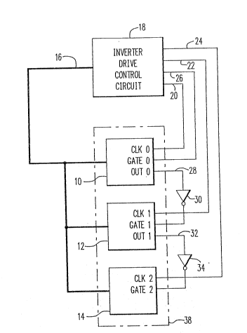
Figure 1 is a block diagram of a circuit
~f ~
4 55,3~2
constructed in accordance with the preferred embodiment of
t~e present invention: and
Figures 2 and 3 show a series of waveforms which
are used to explain the operation of the circuit of Figure
1~
DESCRIPTION OF THE PREFERRED EMBODIMENT
Referring to the drawings, Figure 1 i5 a block
diagram o~ a circuit for measuring the duration of a
selected pulse in a pulse train, such as an in~erter drive
logic pulse train. ~he circuit includes first, second and
third counters 10, 12 and 14 respectively, which receive
various logic signal inputs via data bus 16 from an
inverter drive control circuit 18. The inverter drive
control circuit is part of an inverter system which is
being tested and contains a microprocessor which supplies
data to, and controls the operation of, the three clock
circuits to perform the measurement method of this
invention. In that capacity, the inverter drive control
circuit serves as a controi means for loading the first
counter 10 with a first predetermined initial count N; ~or
loading the second down counter 12 with a second predeter-
mined initial count representative o~ a selected pulse in
an in~erter driva logic signal, the duration of which i5
to be measured; and for loading the third down counter
with a third predetermined initial count, which in the
preferred embodiment is the maximum count of the third
counter. The inverter drive circuit also supplies
inverter drive sync pulses to the first counter via line
20 and inverter drive logic signal pulses to the second
counter via line 22. The microprocessor provides a high
speed clock signal to the third counter via line 24.
In the pre~erred embodiment, the inverter drive
sync signal i5 a high to low transition during the 18th
inverter drive logic pulse. The next high to low
transition of the inverter drive logic signal is defined
as the beginning o~ pulse No. 1.
A start pulse STL is supplied on line 26 to
enable the first counter to count pulses in the sync
h; '.~ ~ ~ 5 ~
5 5~, 342
signal SYNL. The first high to low transition on the sync
~ignal SYNL, after the start pulse STL, produces a pulse
count ena~le signal PCEL on line 28. This signal is
inverted by an inverter 3 0 and supplied to the gate input
of counter 12. This enables counter 12 to count pulse
edges in the inverter drive logic signal IDL supplied by
the inverter drive control circuit 18 via line 22. When
the second counter 12 reaches a predetermined output,
which is zero in the preferred embodiment, it produces a
pulse width enable signal PWEL on line 32 which is
inverted by inverter 34 and serves to enable counter 14
to count the high speed clock pulses supplied via line 24.
After the output of counter 12 goes beyond its predeter-
mined output count, counter 14 stops and its output count
is representative of the duration of the selected pulse in
the inverter drive logic signal. This output count can
then be read via data bus 16 and the duration of the
selected pulse can be easily calculated by the micropro-
cessor in the inverter drive control circuit 18. In the
preferred embodiment, counters 10, 12 and 14 are all
contained in a single, commercially available 82C54
programmable interval timer 38.
In the preferred embodiment o~ Figure 1, counter
10 serves as a hardware/software synchronization circuit
for arming and disarming the rest of the measurement
circuit. Hardware/software synchronization refers to the
fact ~hat the inverter drive sync signal is a function of
the inverter drive logic hardware circuit and the start
pulse, STL, is produced via a set of software instruc-
tions. These two signals are unrelated, and ~herefore
asynchronous, and require synchronization by counter 10.
Counter 12 serves as a pulse counting circuit and counter
14 serves as a pulse width measurement circuit. Counter
10 is employed as a one shot to allow hardware/software
synchronization. This eliminates the need for SR flip
flop circuits which were used to arm and disarm the
previous pulse width measurement circuit. Wh~n configured
as a one shot, the output of counter 10, on line 28, is
6 55,342
activated when the first sync pulse following the start
pulse is received. The output of counter 10 remains
acti~e until enough sync pulses are received for counter
10 to count down below zero. In the preferred embodiment,
N=2, the output of counter 10 is active during a "range"
of counts from 2 down through zero. Counter 12 is used as
a down counter to output a pulse when it reaches a zero
count. This contrasts with the previous measurement
circuit which used an upcounter and a comparator to
perform the same function. Both the present invention and
the previous measurement circuit use a CoUntQr to provide
the pulse width measurement functio~ by counting a high
speed clock signal during the selected pulse. In the
preferred embodiment, counter registers which are internal
to the 82C54 circuit, replace the external pulse count
register used in the previous measurement circuit. Each
counter register is an integral part of one counter stage
of the 82C54. The counter register holds the count for
that counter stage.
In the preferred embodiment of Figure 1, counter
14 is configured in the "interrupt on terminal count
mode". In this implementation, the terminal count (zero)
should never be reached. This counter is enabled by the
output of the pulse count counter 1~. In the preferred
embodiment, counter 14 is clocked by a 3.07 megahertz
clock signal. During the specified pulse, that counter
counts down ~rom its maximum count level, FFFF in
hexadecimal notation, at a 3.07 megahertz rate. After
sending thè start pulse to counter 10, the microprocessor
in the in~erter drive control circuit 18 waits for a
minimum of three sync periods, at which time, counter 14
will contain the pulse width value. The microprocessor
can then calculate the pulse duration according to the
following formula:
T = (2 's Complement of Counter 14)/(3.07 MHz)
where T is the pulse width.
S~ ?~
7 55,342
.
The operation of the circuit of Figure 1 can now
be explained with reference to the waveforms of Figures 2
and 3. To initiate the measurement cycle, a write signal
WRL is supplied via data bus 16 to counters 10, 12 and 14.
5 At time To~ the first pulse in the write signal loads the
pulse width counter 14 with its predetermined initial
count, which in the pre~erred embodiment is FFFF. At
time ~1~ the second pulse in the write signal loads the
pulse counter 12 with its initial predetermined count,
that is representative of the pulse of interest in the
inverter drive logic signal. At time T2, the third pulse
in the write signal loads counter 10 with its initial
count, which in the preferred embodiment is two. At time
T3, a pulse in start signal ST~ initiates the measurement
se~uence. When the first sync pulse in encountered at
time T4, counter 10 is activated to produce a logic low
level output in the pulse count enable signal PCEL. This
enables counter 12 to begin counting negative edges of the
inverter drive logic signal. At time T7, the pulse of
interest is reached and the pulse width enable signal PWEL
at the output of counter 12 goes to a logic low level. At
time T8, the next negative going edge of the inverter
drive lo~ic signal occurs and the pulse width enable
signal re~urns to a logic high level.
Figure 3 showg the pulse width enable signal in
an expanded time scale so that the high speed clock si~nal
CLK can be illustrated along with the count values in
counter 14. Note that the output count of counter 14
begins at FFFF and ends at FFF4. Returning to Figure 2,
at time T11, the second sync pulse negati~e edge (beyond
the initial sync pulse negative edge) is encountered.
This deactivates counter 10, and disables any further
operation of the pulse counter 12 and the pulse width
counter 14~ At this point, the entire circuit is disabled
until the next start pulse is received. At time T12, a
pulse and read signal RDL is used to transfer the output
count from counter 14 to the microprocessor in the
inverter drive control circuit so that the duration of the
8 55,342
.
pulse of interest can be calculated.
Although the present invention has been
described in terms of what is at present believed to be
its preferred embodiment, it will be apparent to those
skilled in the art that various changes may be made
without departing from the scope of the invention. It is
therefore intended that the appended claims cover such
changes.