Note: Descriptions are shown in the official language in which they were submitted.
2024850
Amplifying with Directly Coupled, Cascaded Amplifiers
Background of the Invention
This invention relates to amplifying schemes
which use a number of amplifiers to provide output
voltage and power swings greater than those available
from a single amplifier.
It is known to cascade amplifiers in series,
parallel, or in series/parallel combinations, to
increase the overall voltage swing and power output of
the amplifier arrangement without increasing the
magnitude of the power supply voltages) and also to
facilitate impedance matching to loads.
In some arrangements, for example, those
described in U.S. Patent 4,454,480, issued to Allfather
et al., identical amplifiers are cascaded between a
common (e. g., ground) terminal and an output terminal.
Each amplifier includes a dual polarity power supply,
the common (i.e.) reference) node of which is driven by
the output of the immediately preceding amplifier in the
cascade arrangement. A signal to be amplified is
20~ applied in series to the inputs of the amplifiers.
Typically, the signal is applied between the common node
of each amplifier's power supply and the input of the
amplifier using an isolation amplifier or an isolation
transformer. Because each signal is referenced at the
same potential as the power supply of the amplifier to
which the signal is applied, the source of the signal to
be amplified must be capable of producing voltage swings
that are greater than the voltage swings generated by a
single amplifier.
2024850
- 2 -
Summary of the Invention
The invention features, in general, amplifying a
signal with a plurality of amplifiers, each amplifier
having a reference port and a signal port and each
amplifier being supplied by a power source with operating
potential with respect to a reference node that is
coupled to the reference port of that amplifier; the
amplifiers are cascaded in a manner selected so that the
output of a first amplifier (which receives the signal to
be amplified at its input port) drives the reference node
of a second amplifier, and the reference node of the
first amplifier provides an input at the signal port of
the second amplifier, whereby the first and second
amplifiers are directly coupled together to amplify the
applied signal.
Because the amplifiers (e. g., Class B amplifiers)
are directly cascaded, the need for signal isolation
amplifiers, signal isolation transformers, or other
devices between the amplifiers is eliminated. As a
result, the source of the input signal need not provide a
voltage swing greater than that which can be produced by
a single amplifier. Because each amplifier reproduces
the voltage between the reference node of its power
source (i.e., the output of the previous stage) and the
voltage at the reference node of the previous stage,
input signal voltage and power are both cascaded and
amplified.
In general, the performance parameters of the
amplifiers are additive in this arrangement. For
example, if there are N amplifiers which have identical
unity inverting voltage gains (A~) and identical current
gains (AI), the total voltage gain is N~A~ and the overall
power gain is N multiplied by the power gain of a single
amplifier. For example, if A~ _ -1, the total voltage
2024850
- 3 -
gain is -N. Also, the total slew rate equals N
multiplied by the slew rate of one amplifier. On the
other hand, the overall current pain of the arrangement
equals the current gain of a single stage, and the total
gain-bandwidth is that of a single stage. Moreover, if
the N power supplies for the N amplifiers each supply an
operating potential V, the cascaded amplifiers can
produce an output signal having a maximum (i.e.,
nonclipped) voltage of N~V volts.
Preferred embodiments include the following
features.
The amplifiers are cascaded by electrically
coupling the output of the first amplifier to the
reference port of the second amplifier, and connecting
the reference port of the first amplifier to the signal
port of the second amplifier.
Alternatively, the amplifiers can be arranged
to amplify the input signal in parallel. This is done
by decoupling the .reference port of the second amplifier
from the output of the first amplifier and decoupling
the signal port of the second amplifier from the
reference port of the first amplifier. Instead, the
signal ports of the first and second amplifiers are
coupled together and the outputs of the first and second
amplifiers are also coupled together. In this case, the
reference ports of the first.and second amplifiers are
coupled to a reference (e.g., ground) potential, and
resistances are coupled in series with the amplifier
outputs to compensate for small differences in amplifier
parameters (e. g., gain and offset).
The power sources each convert an applied A.C.
potential to D.C. potentials having opposite polarities
and couple the D.C. potentials to the associated
amplifier. This is preferably done with a power
2024850
- 4 -
transformer that has a primary winding coupled to a
source of A.C. potential and a secondary winding for
developing the D.C. potentials; the secondary winding
includes a center tap that forms the common node of the
power source.
Other features and advantages of the invention
will be apparent from the following detailed
description, and from the claims, with reference to the
accompanying drawings in which:
Brief Description of the Drawings
Fig. 1 is a block diagram of the amplifying
system of the invention;
Figs. 2A-2E are waveforms useful in
understanding the operation of Fig. 1;
Fig. 3 is a schematic diagram of the amplifying
system of Fig. 1;
Fig. 4 is an alternative arrangement of the
amplifying system of Fig. 3; and
Fig. S is a diagram of one embodiment of the
power supplies used in Figs. 1, 3, and 4.
Detailed Description
Referring to Fig. 1, the amplifying system 10
of the invention includes a plurality of (such as four)
amplifiers 12, 14, 16, 18 that are preferably identical
Class B devices. Each amplifier (e.g., amplifier 12)
includes a signal-input port (sig) 20 and a reference
port (ref) 22. The output 24 of each amplifier (e. g.,
amplifier 12) is connected to the next succeeding
amplifier (e. g., amplifier 14) and as a result
amplifiers 12-18 are serially cascaded between input
terminal 26 and output terminal 28.
Amplifiers 12, 14, 16, 18 operate using
dedicated dual-polarity D.C. power supplies 30, 32, 34,
36, respectively, which are each represented in Fig. 1
-202485p
-5-
by a pair of batteries Vss. Each power supply is
arranged to couple potentials of +Vss and -Vss with
respect to its own common node C to the associated
amplifier. The common node C of power supply 30 is
connected to ground potential, while the common nodes of
power supplies 32, 34, 36 "float" above ground.
Amplifiers 12-18 are directly cascaded
according to the invention so that the signal needed to
drive each amplifier is supplied directly by the
preceding amplifier, without the use of any isolation
amplifiers, isolation transformers, or instrumentation
amplifiers between amplifiers 12-18. The output 24 of
each stage drives the floating common node C of the
power supply of the next succeeding amplifier, and the
reference port 22 of each stage is connected to the
signal port 20 of the following stage. For example,
output 24 of amplifier 12 drives common node C of power
supply 32, which is in turn connected to reference port
22 of amplifier.l4. Signal port 20 of amplifier 14 gets
its input directly from reference port 22 of amplifier
12.
This cascading scheme is followed for the
remaining amplifiers in the arrangement. ,Thus, the
output of amplifier 14 is applied to common node C of
power supply 34 and the reference port of amplifier 16,
the signal port 20 of which is connected to reference
port 22 of amplifier 14. Common node C of power supply
36 (and hence reference port 22 of amplifier 18) is
driven by the output of amplifier 16, the reference port
22 of which is tied to signal port 20 of amplifier 18.
The arrangement is completed by connecting input
terminal 26 (which is referenced to ground) to signal
port 20 of amplifier 12, and connecting output port 24
of amplifier 18 to output terminal 28. Output terminal
28 is also referenced to ground.
202485p
- 6 -
Referring also to Figs. 2A-2E, in operation,
let each amplifier have an inverting unity gain. With
an input voltage VIN as shown in Fig. 2A, the output
voltages of amplifiers 12 (V1), 14 (V2), 16 (V3),
and 18 (Vout) are shown in Figs. 2B-2E, respectively.
Each amplifier/power supply stage amplifies the voltage
between its power supply common node C (i.e., the output
of the previous stage) and the common node C of the
power supply of the immediately preceding stage. As a
result, the total voltage gain of amplifying arrangement
10 is the sum of the voltage gains (A~) of individual
amplifiers 12-18 (i.e., 4). That is
Vout 'vl + -v2 + -w3 + --V4
VIN
Also, because amplifiers 12-18 are identical and
connected in series, current gain (AI) of arrangement
10 equal those of a single amplifier. Accordingly,
I1 _ I2 = I3 _ I4
It is thus seen that the power gain is also additive,
the total power gain equalling the power gain of an
individual amplifier multiplied by the number of
cascaded amplifiers.
Note also from~Figs. 2B-2E that, although each
amplifier 12-18 operates from a power supply of +Vss'
all amplifiers except for initial amplifier 12 can
produce outputs having greater voltage-swing than +Vss
without clipping. This is because of the serial
cascading of amplifiers 12-18. In general, (assuming
equal Vss magnitudes for all power supplies) the
maximum voltage swing of the arrangement is equal to the
number of amplifiers multiplied by the maximum voltage
swing (+Vss) of one amplifier. Thus, amplifier 14 can
generate an output of +2Vss, an output of +3Vss can
be produced by amplifier 16, and the total voltage swing
of arrangement 10 (at output terminal 28) is +4Vss'
2o24s5Q
-,_
Other advantages follow from serially cascading
amplifiers 12-18 as in Fig. 1. For example) the slew
rate of arrangement l0 becomes the slew rate of a single
amplifier multiplied by the number of amplifiers.
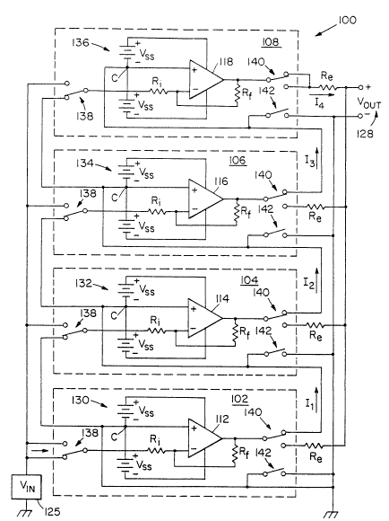
Referring to Fig. 3, a specific circuit 100 for
implementing amplifying arrangement 10 (Fig. 1) is
shown. Amplifying system 100 comprises a plurality of
(such as four) identical amplifier circuit sections 102,
104, 106, 108. Sections 102-108 respectively include
differential amplifiers 112-118 and power supplies
130-136. Each power supply 130-136 is represented by a
pair of batteries connected to provide operating
potentials of _+Vss (with respect to a common power
supply node C) to the associated amplifiers 112-118.
Each amplifier section 102-108 also includes a
set of switches 138, 140, 142 for cascading sections
102-108 between a source 126 of input voltage (VIN)
and an output terminal 128.
One switched terminal of switches 138 in
sections 108, 106, 104 is connected to input voltage
source 126, and the other switched terminal of each such
switch 138 is connected to the common node C of the
power supply 134, 132, 130 of the immediately preceding
amplifier section 106, 104, 102, respectively. Hoth
switched terminals of switch 138 in amplifier section
102 are connected to source 126.. _
Amplifiers 112-118 are operational amplifiers
having a gain of -1 as determined by resistors Ri and
Rf. The inverting (-) input of each amplifier 112-118
(e. g., amplifier 114) is driven from the common terminal
of switch 138 in its amplifier section (e. g., section
104) and the noninverting (+) input provides a reference
and is connected to the common node C of the amplifier's
power supply (e. g., power supply 132).
. 2024850
_$_
Amplifiers 112-116 drive either the next
succeeding amplifier 114-118, respectively, or output
terminal 128 via switches 140. More specifically, the
outputs of amplifiers 112, 114, 116 are connected to the
floating common nodes C of power supplies 132) 134, 136,
respectively, when switches 140 are in the position
shown in Fig. 3. When switches 140 are in the opposite
position (as shown in Fig. 4, discussed below),
amplifiers 112-118 drive output terminal 128 in parallel
through resistors Re. The output of amplifier 118
always drives output terminal 122 through its switch 140.
Amplifying system 100 is referenced to the same
potential (e.g., ground) as voltage source 126. To
establish this reference potential, the common node C of
power supply 130 (and hence the noninverting (i.e.,
reference) input of amplifier 112) is always connected
to ground potential, either directly or through switch
142. Switches 142 operate in tandem with switches 140
to alternatively. connect the common nodes C power
supplies 132-136 to ground potential when amplifiers
112-118 are to operate in parallel (as explained below
in connection with Fig. 4).
In operation, with switches 138, 140, 142 all
in the positions shown in Fig. 3, amplifiers 112-118 are
serially cascaded between voltage source 126 and output
terminal 128 and operate in the same manner as described
above for amplifying-system 10: Amplifying system 100
thus has a total voltage gain of -4 (i.e., the sum of
the four inverting unity gains of amplifiers 112-118).
On the other hand, the output currents I1-I4 of
amplifiers 112-118, respectively, are all equal. That
is, the total current gain of system 100 equals the
current gain of a single amplifier. The maximum voltage
swing of the output signal produced at terminal 128 is
+4Vss, as discussed above.
2024850
_ g _
Referring to Fig. 4, when switches 138, 140,
142 are all actuated to their opposite positions,
amplifiers 112-118 are cascaded in parallel between
voltage source 126 and output terminal 128 through
switches 138, 140. Also, the common node C of each
power supply 130-136 (and thus the noninverting input of
each amplifier 112-118) is connected to ground potential
through switches 142. As a result, the total voltage
gain of system 100 becomes that of a single amplifier
(i.e., -1). On the other hand, the output currents
I1-I4 add, and hence the total current gain is four
times the current gain of each amplifier 112-118.
Resistors Re are present to compensate for
small differences in the parameters (such as gain and
offset) of amplifiers 112-118. The closer that the
amplifiers are matched, the smaller equalizing resistors
Re may be. As the resistances of resistors Re
decrease, so, too, are the errors and deficiencies that
they cause reduced.
Other embodiments are within the following
claims.
For example, although four amplifiers have been
shown, more or fewer amplifiers can be cascaded in
accordance with the invention.
Referring to Fig. 5, power supplies 30-36,
- 130=136-can'each be implemented-by-fnll-wave rectifying
an A.C. signal from source 150 using a transformer 152
having a center tapped secondary winding 154 and a diode
bridge 156. The center tap becomes the common node C of
the power supply and also serves as the reference for
D.C. supply voltages +Vss and for ripple capacitors
158.