Note: Descriptions are shown in the official language in which they were submitted.
~2~
DOCKET R4378.01
EAO:cjf
1 IMPROVED FLAT PANEL DISPLAY SYSTEM AND METHOD
.
2 BACKGROUND OF THE INVENTION
3 This invention relates to flat panel
ll displays generally and, more particularly, -to a novel
flat panel display sys-tem, and rnethod, that employs
6 demultiplexing to direct selected light inputs through
7 optical fibers -to appropriate pixel locations on the
8 flat panel display.
9 Conventional flat panel displays may be of
the liquid crystal type which have, as particular
11 disadvantages, a rather narrow viewing angle and a
12 limited operating temperature range. Others may be of
13 the gas plasma or the electroluminescent types, both
14 of which suffer the disadvantage of requiring high
electrical potential and power consumption for
16 operation, thus presenting a safety hazard as well as
17 necessarily requiring components capable of handling
18 the voltage levels involved. A Further disadvantage
19 of all of the above types of prior art flat panel
displays is that each requires the use of rela-tively
21 expensive components.
-- 1 --
1 I-t is, therefore, an object of the present
2 invention to provide an împroved flat panel display
3 system which offers hiyh resolution, yet is of
4 relatively inexpensive to construct.
It is another object of the invention to
6 provide such a display which has low power consumption
7 and employs relatively low electrical potentials.
8 It is a further object of the invention to
9 provide such a display which makes multiple use of
individual illumination sources for the display.
11 SUMMARY OF THE INVENTION
12 The present invention substantially
13 overcomes the limitations of conventional devices and
14 achieves the above objects, among others, by providing
an improved flat panel display in which the pixels
16 thereoF are illuminated by optical fibers. Economy
17 and compactness are achieved by using micromechanical
18 light modulat3rs to demultiplex light from a limited
19 number of LED's to a large number of pixels. ~ith the
use of micromechanical light modulators incorporated
21 on an integrated circuit, the flat panel display
22 system is relatively economical, has low power
23 consumption, and produces a display of very high
24 resolution. The display may be provided in full color.
-- 2 --
~2~a~
1 For a better understanding of the present
2 invention, together with other and further objec-ts7
3 reference is made to -the following description, taken
4 in conjunction with the accompanying drawings, and its
scope will be pointed out in the appended claims.
6 BRIEF DESCRIPTION OF THE DRAWIN~S
7 Fig. 1 is a schematic perspective
8 representation of a portion of a flat panel display
9 system showing alternative means of pixel
illumination, according to the present invention.
11 Fig. 2 is a schematic representation of a
12 "daisy chain" light demultiplexer useful in the system
13 of Figure 1.
14 Fig. 3 is a schematic represen-tation of a
"tree" demultiplexer useful in the system of Figure 1.
16 Fig. 4 illustrates an array of
17 micromechanical light modulators by which 640 pixels
18 of a display may be illuminated by 10 light sources,
19 according to the present invention.
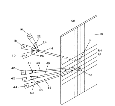
QETAILED DESCRIPTION OF THE INVENTION
21 Fig. 1 is a perspective, schematic,
22 fragmentary representa-tion of a flat panel display
23 system according to the present invention, which
24 includes a flat panel 10 formed from a light difFusing
material such as ground glass. If desired, flat panel
~ J 2 ~
1 10 may be clear with a layer of phosphorluminescen-t
2 material thereon to provide an appropriate time
3 constant in -the decay of the illumination. It will be
4 understood that the area of display 10, as is true
with conventional displays, is divided into a large
6 number of picture element areas, or pixels, the
7 location of each being defined by its assignment to a
8 specific imaginary column and row on the display, such
9 as pixel 12 the location of which is defined by its
being located in imaginary Column M and Row N. The
11 orthogonal lines shown on panel 10 in fig. 1 will be
12 understood as being imaginary and are shown solely for
13 convenience in describing pixel locations,
14 Illumination at pixel 12 is provided by
the termination thereat of an optical fiber 14.
16 Optical fiber 14 is optically coupled at its other end
17 to red light source 16, green light source 18, and
18 blue light source 20, the wavelengths of those light
19 sources corresponding~ respectively, to the three
primary colors. Lenses 22, 24, and 26 may be disposed
21 between light sources 16, 18, and 20, respectively, if
22 necessary, -to assist in coupling light from the
23 sources to the end of optical fiber 14. The color (or
24 black or white) appearing at pixel 12 will depend on
which or all Gf light sources 16, 18, and 20 are on or
26 off and the relative intensity of the individual light
-- 4 --
~ 3 ~
1 sources. This may be controlled via the control means
2 52 shown in Figs. 2 and 3. It will be understood -that
3 similar optical fibers and similar light sources would
4 be provided for each of the other pixels on display 10.
An alternative rnethod of providing
6 illumination at a pixel is shown in Fig. 1 where
7 illumination of a pixel 32, located in Column M and
8 Row P, is provided by three separate optical fibers
9 34, 36, and 38, which are coupled to primary color
light sources 40, 42, and 44, respectively, through,
11 if necessary, lenses 46, 48, and 50, respectively. In
12 this case, the ends of optical fibers 34, 36, and 38
13 at pixel 32 are so closely spaced that the
14 illumination by the optical fibers is combined in the
eye of the viewer when the viewer is positioned at
16 normal distances from display 10 so that the same
17 effect is achieved as at pixel 12 where the single
18 optical fiber 14 terminates at pixel 12. Again, if
19 this method is provided, each pixel on display 10 will
be provided with three optical fibers. This means, of
21 course, that three -times as many optical fibers are
22 required; however, this method avoids having to couple
23 the light to the optical fibers at an angle.
24 Although the above systems have been
described in terms of providing a full color display,
26 the display may instead be provided simply in
27 black~and-white or monochrome.
~ ~ 2 ~
1 In the above system, ligh-t sources 16, 18,
2 20, 40, 42, and 44 may be individual light sources,
3 such as LED's, lamps, or lasers, for example; however,
4 it will be appreciated that such would require a very
large number of ligh-t sources.
6 Fig. 2 illustrates one means by which a
7 single light source may be used to provide
8 illumination to a plurality of pixels on a display
9 through the use of micromechanical light switches, or
modulators. The operation and construction of such
11 devices are described in the article "Micromechanical
12 light modulators on silicon," by Robert E. Brooks,
13 printed in OPTICAL ENGINEE~ING, January/February 1985,
14 Vol. 24, No. 1, beginning at page 101, which article,
and the references cited therein, are made a part
16 hereof by reference. An improved form of
17 electromechanical light modulator useful in
18 implementing the present invention is disclosed in my
19 co-pending U. S. Patent Application Serial
No. 07/411,969, filed September 25, 1989 and assigned
21 to the same assignee~ Basically, the micromechanical
22 light modulator comprises a reflective metal-coated
23 silicon dioxide paddle which is can-tilevered over a
24 well into which it can be deflected by an electrical
charge on a substrate under the paddle. The angle of
26 reflection is determined by the magnitude of -the
27 charge and a number of deflection angles can be
resolved with a single paddle. An important feature
2 of the modulators is that they can be formed as part
3 of an integrated circuit and disposed in high
4 density. For example, in a 2 X 18 array described,
5 the paddles are 60 microns square, 0.6 microns thick
6 over 5-micron deep wells, and spaced on 87.5-micron
7 centers. Each of the paddles is electronically
8 selectively addressable. It will -thus be understood
9 that a very large number of such modulators may be
10 provided compactly on an integrated circui-t and the
11 voltage and power requirements are inherently low.
12 Because of the smallness of all of the compents 9 -the
13 system can be readily configured as a flat panel
14 display.
Referring again to Fig. 2, a light source
16 60, which may be assumed to be an LED producing one of
17 the prlmary colors, is disposed so as to provide
18 illumination to the end of an optical fiber 62. The
19 other end of optical fiber 62 is disposed so that the
20 beam of light therefrom is incident upon
21 micromechanical light modulator 64, which, when the
22 modulator is in the position shown in solid lines,
23 reflects the light beam so tha-t it is coupled to one
24 end of optical fiber 66. But, when the modulator is
25 in the position shown in dashed lines, the light beam
26 is coupled to the end of optical fiber 68. If coupled
27 to optical fiber 68, the light bearn is transmitted to
1 a flat panel display (not shown). If, however, -the
2 light beam is coupled to optical fiber 66, it is
3 transmitted to another micromechanical light modulator
4 70 where, in similar fashion, the light beam may be
coupled either to optical fiber 72 for transm.issiorl to
6 the flat panel display or to an optical fiber for
7 transmission to yet another micromechanical light
8 modulator 76. If the latter, then micromechanical
9 light modulator 76 will couple the light beam to
either one of optical fibers 78 or 80, and so forth,
11 for all or part of a row or column of pixels or even
12 multiple rows and/or columns. The operation oF the
13 light modulators 64, 70 and 76, and the light source
14 60, is controlled by control means 52 so as to display
information desired on the display screen. For the
16 full-color displays described above, there would be
17 provided a red-green- blue trio of such ~Idaisy chains"
18 coupled to pixel 12 or pixel 32 (Fig. 1). Since -the
19 micromechanical modulators can operate at frequencies
up to about 1 MHz., one light source can
21 satisfactorily provide illumination to a large number
22 of pixels, with the viewer's eye integrating the light
23 from the display so that the multiplexed operation is
24 not apparent.
One disadvantage of the daisy chain
26 approach is that the intensity of the light beam
27 decreases by a certain increment each time it is
_ ~ _
~2~
reflected. Therefore, if the ligh-t beam were switched
2 to the display early in the chain, it would have a
3 greater intensity than if it were switched to the
4 display later in the chain. This disadvantage can be
eliminated if the "tree" configuration demultiplexer
6 shown in Fig. 3 is employed~ Here, following only one
7 branching of the "tree," light source 90 provides
illumination to one end of optical fiber 92 which
9 transmits the light beam to micromechanical light
modulator 94, which in turn couples the light beam to
11 a selective one of five optical fibers, here, -For
12 example, optical fiber 96. Optical fiber 96 transmits
13 the light beam to micromechanical light modulator 98
14 which, in turn, couples the light beam to optical
fiber 100, for example, and so forth, to
16 micromechanical light modulator 102, optical fiber
17 104, micromechanical light modulator 106, and to
18 optical fiber 108 which transmits the light beam to
19 the display.
Thus, with the tree demultiplexer
21 configuration of Fig. 3, a single light source9 LED
22 90, provides illumination to any of 625 pixels under
23 the control of control means 52. Of course, a tree
24 demultiplexer may be constructed to serve a larger or
smaller number of pixels, fig. 3 being for
26 illustrative purposes only. In any case, use of the
27 tree demultiplexer assures that all light beams are
_ g
switched an equal number of times before reaching the
2 display.
3 Fig. 4 shows how the micromechanical ligh-t
4 modulators oF the tree conFiguration demultiplexer o-F
Fig. 3 may be constructed. Here, an array 120 of
6 micromechanical light modulators, which may be assumed
7 to be formed on the surface of an integrated circuit
8 as an integral part thereoF, such as micromechanical
9 light modulator 122, has the modulators rec-tilinearly
arranged in rows Rl - ~10 and columns Al, ~1 - B~, and
11 Cl - C16. Whereas in the tree demultiplexer of F.ig.
12 3, each micromechanical light modulator optically
13 coupled the light output of one optical fiber to a
14 selected one of five other optical fibers, on array
120 each micromechanical light modulator optically
16 couples the light output of one optical fiber to a
17 selected one of four other optical fibers (none of the
18 optical fibers are shown in Fig. 4). It will be
19 understood, then, for example, tha-t the
micromechanical light modulator at column Al and row
21 Rl will optically couple a light source to any
22 selected one of four optical fibers which lead to the
23 micromechanical light modulators at columns al ~ B~
24 and row Rl. Each one of four latter micromechanical
light modulators will, in turn1 couple the lignt -to
26 any selected one of four optical fibers which lead to
27 four of the micromechanical ligh-t modula-tors at
-- 10 --
1 columns Cl - C16 and row Rl, which, in turn, will
2 couple the light to corresponding pixels on the
3 display panel (not shown). Thus, with array 120, only
4 ten light sources may be used to illuminate a total of
640 pixels (((lOX4)X4)X4).