Note: Descriptions are shown in the official language in which they were submitted.
-- 202~1 64
B~CKGROUND OF IXE INVENTION
The present invention relates to a phase lock loop (PLL) for
carrier regeneration, and/or clock regeneration in radio
5 communication and satellite communication systems.
In digital radio communication and satellite communication
systems using PSK (Phase Shift Keying) modulation, a receiver
demodulates a PSK signal through a coherent detection which has
excellent demodulation characteristics for transmission errors. In
10 the coherent detection, a demodulator must have an accurate
carrier which synchronizes with the phase of the transmitted
carrier, and also has the same frequency as that of the transmitted
carrier. To regenerate the carrier in the receiver, a PLL or a tuning
circuit has been used.
In a mobile communication system, andtor a satellite
communication system, there is a high channel noise, a large
frequency offset, and a frequency shift caused by a doppler effect
in the carrier frequency. These factors degrade the performance of
the carrier recovery, and it is sometimes difficult to regenerate a
2 0 stable carrier, resulting in a synchronization loss in such systems.
Also, the PLL takes a long time to complete the pull-in and lock-in
stages, and also the PLL falls out of lock often even after the PLL
locked in.
To solve the above problems, it has been proposed to use a
2 5 preamble long enough for the carrier regeneration. However, the
transmission efficiency decreases. Further, if the synchronization
loss in the system happens once because of the channel noise,
fading disturbances, or the frequency shift after the
-` 202S164
synchronization is established, no carrier regeneration is
possible in the receiving side, since no preamble is obtained.
In a low rate radio packet transmission system, no
preamble is attached to a packet in view of transmission
efficiency. In this system, the PLL which acquire the lock-in
quickly and stably, and hold it tightly under a low C/N (Carrier
to Noise power ratio) condition having a high noise has not been
found.
BRIEF DESCRIPTION OF THE DRAWINGS
The present invention will become better understood by
means of the following description and accompanying drawings
wherein;
Figure 1 is a block diagram of a prior carrier
regeneration system using a phase lock loop,
Figure 2A is a block diagram of an adaptive phase lock
loop according to the present invention,
Figure 2B is a block diagram of a mode control 18,
Figure 2C is a block diagram of another embodiment of
a mode control (18),
Figure 2D is a block diagram of a part of an initial
phase difference calculator and a part of a center frequency
difference calculator,
Figure 3 is a block diagram of a lowpass filter (22)
in Figure 2,
Figure 4 is a block diagram of another adaptive phase
lock loop according to the present invention,
~..~,
A
-- 202~164
Figure 5 is a block diagram of a carrier regeneration
system according to the present invention,
Figure 6 is a block diagram of another carrier
regeneration system according to the present invention, and
Figure 7 is a block diagram of still another carrier
regeneration system according to the present invention.
DESCRIPTION OF PRIOR ART FIGURE 1
Figure 1 shows a block diagram of a prior carrier
regeneration system which uses a digital PLL. A PSK modulation
signal is applied to an input terminal (1) and is processed by
a frequency multiplier (2) to generate a carrier component which
is an integer multiple of a carrier frequency. The frequency
multiplier (2) denotes a frequency doubler in case of two phase
modulation, and a tripler in case of four phase modulation. The
output of the frequency multiplier (2) is then applied to the
conventional PLL (5) through the bandpass filter (3) from the PLL
input terminal (4). The PLL (5) provides a VCO output which is
locked-in with the carrier component and is free from the channel
noise, and is obtained at the output terminal (6). The frequency
divider (7) divides the frequency of the VCO output, and provides
the regenerated carrier at the output terminal (8).
It should be appreciated in Fig. 1 that the input
signal is supposed to be a digital signal, and all the elements
in figures described in this invention operate in digital.
The PLL (5) has a phase detector (10) which detects the
phase error between the input signal at the terminal (4) and the
reference signal of the VCO output, a loop filter (11) coupled
with the output of the phase detector (10), and a digital voltage
2a
A
-- 202~164
controlled oscillator of VCO (9) as a reference signal generator.
The VCO (9)
,
1 0 ~/'
i
Z O ,/
/
2b
~'
2025164
consists of an accumulator (12), a center frequency generator (13),
an initial phase generator (14), a cosine converter (15), and adders
(16 and 17). The phase detector (10) receives the reference signal
of the VCO output having a cosine waveform with the initial phase
5 ~o and the center frequency Wo, and the input signal having the
carrier component from the input terminal (4). The phase
difference and/or the frequency difference between the VCO output
and the input signal is detected as the phase error by the phase
detector (10), and then the output is applied to the loop filter (11)
10 which suppresses undesired noise component. The bandwidth and
gain of the PLL loop determines the performance of the pull-in and
the lock-in.
The frequency of the VCO (9) is determined by the error
signal from the loop filter ( 1 1 ) and the output of the center
l S frequency generator (13) which provides a signal corresponding to
the center frequency. The phase of the VCO (9) is also determined
by the output of the accumulator ( 12), and the output of the initial
phase generator (14) which provides a signal corresponding to the
initial phase. The error signal from the loop filter (11) is added to
2 0 the output of the center frequency generator (13) through the
adder (16), and then is fed to the accumulator (12) which
accumulates it at every sampling time. The output of the
accumulator (12) is added to the output of the initial phase
generator (14) through the adder (17), and then is fed to the cosine
2 5 converter (15) which generates a cosine waveform as the VCO
output. The output of the VCO (9) is applied to the phase detector
(10) as a reference signal to the input signal. The locked VCO
output is obtained at the output terminal (6), and the output
frequency is divided by the frequency divider (7) which provides
202~16~
the regenerated carrier. The VCO (9) operates first to complete the
pull-in stage for coinciding the frequency, and next to complete
- lock-in stage for the phase lock.
Since the circuit elements operate in digital, it should be noted
5 that the center frequency generator (13) and the initial phase
generator ( 14) provide a constant level corresponding to the center
frequency and the initial phase, respectively. When the
accumulator (12) accumulates the constant level signal
corresponding to the center frequency at every sampling time, the
10 output of the accumulator (12) becomes a ramp signal increasing
with time. -Also ~ the accumulator (12) outputs a constant level
signal to compensate the initial phase to the phase of the input
signal. The initial phase generator (14) prepares the constant level
signal corresponding to the initial phase to determine the initial
15 phase of the VCO. The cosine converter ( 1 5) converts the input to
the cosine waveform in a digital form. The output of the loop filter
eventually adjusts the frequency and the phase of the VCO output
through the accumulator (12) instantaneously. Therefore, it should
be appreciated that the VCO (9) in Fig. 1 performs just as a
2 0 conventional analog voltage controlled oscillator.
The frequency multiplier (2) increases the noise level by 6 dB
in BPSK, and the phase detector (10) using a multiplier also
generates some additional noise caused by the non-linear operation.
Noise causes the pull-in and lock-in times longer, and further
2 5 causes the out of lock after the lock-in state was achieved once.
Therefore, when the C/N is very low, a stable carrier regeneration
becomes difficult. Particularly, when a frequency offset and/or a
frequency shift are large, the above problem becomes more serious.
When the loop gain of the PLL (5) is high, the pull-in and the
P~ 4
202~16~
-
lock-in times are short, however the sensitivity to noise becomes
high, resulting in a large phase jitter and a frequency jitter in the
VCO output at the terminal (6). On the other hand, when the loop
gain of the PLL (5) is low and the bandwidth of the loop is narrow
to remove the noise, the pull-in and lock-in capabilities for the
frequency offset and the initial phase difference become low,
resulting in narrower pull-in and lock-in ranges. Accordingly, it is
difficult for the loop to lock, and a carrier loss happens. For
example, when the value of the C/N is lower than 3 dB, it is almost
impossible to regenerate the stable carrier in a prior art. Further,
the prior phase detector using a multiplier has a disadvantage of a
false lock.
The narrow bandwidth of the loop would have the
disadvantage of taking a long time to achieve the lock-in state for
the large frequency offset, and of being difficult to hold the lock-in
state for the frequency shift. Conventionally, some improvements
in the performance have been achieved by adjusting the bandwidth
and gain of the loop, depending on whether it is before or after the
lock-in stage, and/or by using a phase detector having a linear
2 0 phase detection characteristics. For instance, the bandwidth of the
loop is first set wider at the kick-off stage, considering the
frequency offset, and then the bandwidth of the loop is switched
narrower to avoid the out of lock state due to noise after the pull-in
condition is established.
2 5 However, the mere switching of the loop gain and/or the
bandwidth is insufficient to achieve a stable carrier recovery in an
extremely low C/N condition having a large frequency offset in
mobile satellite communications.
2~2~16~
Further, a prior tuning circuit cannot regenerate the carrier in
case of the large frequency offset, and/or the large doppler
frequency shift.
1 0
2025164
SUMMARY OF THE INVENTION
It would be an advantage to provide a phase lock loop
which completes a lock-in state widely and quickly under the
conditions having a high input noise and a large frequency
offset, and/or a large frequency shift.
The present invention provides an adaptive phase lock
loop system comprising:
an adaptive phase lock loop system comprising:
a buffer memory for storing a digital input signal;
a phase detector for comparing a phase of the digital
input signal and a phase of a reference signal;
a loop filter coupled with an output of the phase
detector;
a digital voltage controlled oscillator providing a VCO
output as the reference signal to the phase detector, the digital
voltage controlled oscillator including
a center frequency generator providing a
center frequency of the digital voltage
controlled oscillator,
a first adder to provide a sum of an output
of the loop filter and an output of the
center frequency generator,
an accumulator accumulating an output of the
first adder,
an initial phase generator providing an
A
2025164
initial phase of the digital voltage
controlled oscillator,
a second adder providing a sum of an output
of the accumulator and an output of the
initial phase generator,
a cosine converter converting an output of
the second adder to a cosine waveform for
providing the reference signal of the VCO
output,
an initial phase difference calculator,
coupled with the output of the loop filter,
the initial phase difference calculator
updating the initial phase output from the
initial phase generator according to the
output of the loop filter,
a center frequency difference calculator,
coupled with the output of the loop filter,
the center frequency difference calculator
updating the center frequency output from
the center frequency generator according to
the output of the loop filter, and
a mode control means for switching an
operation state between an initial training
mode and a normal operation mode;
wherein the initial training mode repetitively adjusts
the initial phase and the center freguency of the initial phase
difference calculator and the center frequency different
calculator so that the initial phase and the center frequency
202~164
become optimum to complete a lock-in state for the input signal
of the buffer memory, respectively, and the normal operation
mode providing a reference signal of the VCO output so that the
reference signal is phase-locked with the input signal by using
the initial phase and the center frequency optimized in the
initial training mode. -
~/
,/
1 0 ",
,'
//
/
/
- 2025164`-
DESCRIP~ION OF THE PREFERRED EMBODIMENTS
- (Embodiment 1 )
It is assumed that the input signal is in a digital form, and the
PLL handles the digital signal. An A/D converter and a D/A
converter which are used for converting analog signals and digital
signals are not described as they are no concern with the present
invention.
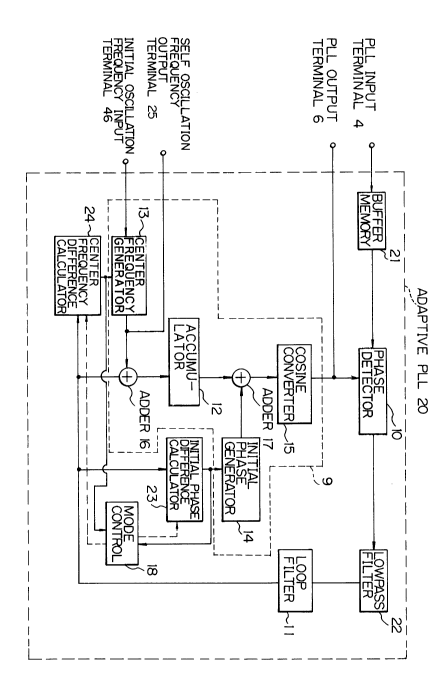
Figure 2A shows a block diagram of an adaptive PLL
according to the present invention. The same numerals as those in
Fig. 1 show the same elements.
The important feature of the present adaptive PLL (20) is the
presence of a buffer memory (21) which stores an input signal from
the input terminal (4), a lowpass filter (2 2 ) for removing noise, an
initial phase difference calculator (23), a center frequency
difference calculator (24), and a mode control (18) for switching the
operation state between the initial training mode and the normal
operation mode. The numeral 25 shows the output terminal of the
center frequency of the adaptive PLL (20).
The operation of the apparatus of Fig. 2A has two modes. The
initial training mode is the initial training stage to search an
optimum initial phase and an optim-um center frequency at the
kick-off. During this mode, the processes to lock the PLL to the
frequency and phase of the input signal are carried out repetitively
2 5 for the same input signal stored in the buffer memory (21),
adjusting the center frequency Wo of the generator (13) and the
initial phase ~o of the generator (14). The normal operation mode
is the ordinary PLL operation stage, in which the center frequency
- generator (13) and the initial phase generator (14) start to operate
A - lO
202~164
with the optimum initial phase and the optimum center frequency
determined in the initial training mode, and the PLL operation is
carried out for the input signal as the conventional manner in Fig. 1.
The output terminal (6) provides the VCO output which is locked-in
S with the carrier component in the input signal.
In other words, the operation of Fig. 2A is the same as that of
Fig.l except that the center frequency of the generator (13) and the
initial phase of the generator ( 14) are adaptively controlled at the
kick-off to lock the VCO output with the stored input signal in the
buffer memory (21) through training the PLL processes, while the
center frequency and the initial phase in Fig. 1 are always fixed
during the operation. The training for optimizing the center
frequency and the initial phase to complete the lock-in is carried
out repetitively for the same input signal which is stored in the
buffer memory (21) in the adaptive PLL (20). The optimum center
frequency and initial phase are obtained by estimating the initial
phase difference and the center frequency difference in the initial
phase difference calculator (23) and the center frequency
difference calculator (24), respectively.
2 0 The operation of the adaptive PLL (20) according to the
present invention is now described in detail.
( 1 ) An input signal to the PLL input terminal (4) is stored in
the buffer memory (21) in a digital form. The memory (21)
functions to provide the same digital signal repetitively in the
2 5 initial training mode until the initial phase error given by the initial
phase difference calculator (23) and the center frequency error
given by the center frequency difference calculator (24) reach less
than predetermined threshold values which denote optimum in the
lock-in condition, respectively, or alternatively the initial training
- 2025164
mode is repeated by the predetermined times which recognizes to
achieve the optimum lock-in condition.
- (2) In the initial training mode, it is assumed that the initial
phase ~o and the center frequency Wo are initially predetermined
5 as ~Oint and Woint~ respectively. The initial values ~Oint and
Woint may be prepared inside the PLL, or alternatively, Woint may
be supplied from an external apparatus which has a spectrum
analyzer by using a linear prediction technique or other technique.
The input terminal (46) is used for the external initial value for the
10 center frequency, if necessary.
(2-1) First, the phase detector (10) detects the phase error
between the input signal in the buffer memory (21) and the phase
of the VCO output fed from the cosine converter (15). The output of
the phase detector ( 1 O) is then applied to the loop filter ( 11 )
15 through the lowpass filter (22). Those filters suppress the noise
component.
(2-2) Next, the error signal from the loop filter (11) is applied
to the phase difference calculator (23) and the center frequency
difference calculator (24). The adder (16) provides the sum of the
20 output of the center frequency generator (13) and the loop filter
(11), and then the sum is applied to the accumulator (12).
(2-3) The outputs of the accumulator (12) and the initial
phase generator (14) are added at the adder (17), and the output is
applied to the cosine converter (15). The cosine converter (15)
2 5 generates a cosine waveform based upon the accumulator output
and the initial phase.
When there is a difference between the frequency of carrier
component of the input signal at the input terminal (4) and the
center frequency of the VCO, the loop filter ( 15) provides a
A
2025164
DC(direct current) component in the error signal depending on the
frequency difference. The DC component in the error signal is
- detected in the frequency difference calculator (24). Similarly,
when there is a phase difference between the phase of the input
5 signal and the initial phase of the VCO, the loop filter ( 11 ) provides
an impulsive error signal which has some amplitude and width in
some duration just after the kick-off. During the duration, the error
signal caused by the frequency difference is small. Accordingly, the
amplitude of the impulsive error signal mainly depends upon
10 the value of the initial phase difference, and the amplitude
decreases as the phase becomes in-lock. In the initial phase
difference calculator (23), the initial phase error between the
phases of the input signal and the VCO output is roughly estimated
by the averaged amplitude of tne impulsive error signal in a short
15 duration after the kick-off.
The initial phase provided by the initial phase generator ( 14)
is updated by the initial phase difference from the initial phase
difference calculator (23), and the center frequency provided by
the center frequency generator (13) is also updated by the center
2 0 frequency difference fed by the center frequency difference
calculator (24). Then, the PLL operation is carried out again for the
same input signal which is stored in the buffer memory (21), by
using the updated initial phase and the updated center frequency.
The calculators (23) and (24) provide values of the initial phase
2 5 difference and the center frequency difference for the next
- updating. The above operation is repeated by the times until it is
presumed that the lock-in state is established. The optimum center
frequency and initial phase are obtained finally.
13
A
202516~
When the initial training mode finishes, the mode is switched
to the normal operation mode, according to one of the following
- ways .
a) The initial training mode finishes when a predetermined
5 number of trials for updating of the phase and the center frequency
are carried out, or the initial phase and center frequency errors are
minimized and are reached predetermined threshold values,
respectively.
b) An input signal is divided for every predetermined
10 number of frames. The initial training mode is carried out for each
frame, or for every predetermined number of frames, so that the
initial phase and the center frequency are adjusted in - each
frame. Then, the mode is switched to the normal operation mode.
c) A lock-in detector is prepared for recognizing the lock-in
15 state. The lock-in state may be recognized by the level of the
lowpass-filtered quadrature phase error (or the level of in-phase
component) between the VCO output and the input signal.
d) The fourth method is that if the lock-out state happens in
the normal operation mode, the initial training mode may be
2 0 carried out again to attain the optimum initial phase and center
frequency, and then switchover to the normal operation mode
again.
e) For the channel having a wide frequency offset, a plurality
of bandpass filters are provided for splitting the transmission band
2 5 of the output signal of the multiplier (2), and the adaptive PLL (20)
is coupled with all or a part of the bandpass filters. In each PLL, a
plurality of initial values of the center frequencies are prepared,
each having a predetermined step of difference in the initial center
frequency. Each initial center frequency is applied to the center
14
202~164
frequency generator (13) through the terminal (46), and the initial
training mode is carried out. When the optimum center frequencies
for all the initial center frequencies become almost the same as one
another, or the differences in the optimum center frequencies are
5 minimum, it is recognized that there is a frequency which
corresponds to the carrier component, and the adaptive PLL of the
related band is switched to the normal operation mode.
It should be appreciated that the bandwidth of the lowpass
filter (22) and/or the loop filter (11) may be set narrower for each
10 training operation in the initial training mode, or when the initial
training mode finishes. The narrow bandwidth of the loop
improves the robustness of the PLL to noise without sacrifice the
pull-in and lock-in ranges, because of the optimum initial phase and
the optimum center frequency.
(3) After the initial phase and the center frequency are
optimized in the initial training mode, the mode is switched to the
normal operation mode with those optimum values.
In the normal operation mode, the phase detector (10) detects
the phase error between the input signal and the VCO output, and
2 0 the output of the phase detector (10) is applied to the adder (16)
through the lowpass filter (22) and the loop filter ( 1 1). The loop
gain and the bandwidth of the loop filter (11) may be also adjusted
during the operation.
It should be noted, therefore, that the initial phase difference
2 5 calculator (23) and the center frequency difference calculator (24)
do not operate in the normal operation mode.
It should be appreciated that Fig. 2A of the present invention
has the feature of the presence of the initial phase difference
calculator (23) and the center frequency difference calculator (24).
~2~164
These calculators obtain the optimum initial phase and the optimum
center frequency in the initial training mode so that the
synchronization system is tremendously improved in noise
performance by using a narrower loop band and a lower gain in the
S PLL loop, and has equivalently a wide pull-in and lock in ranges. It
is also easy to find the frequency offset and the initial phase offset
in the input signal from the optimum center frequency difference
and the optimum initial phase difference.
The frequency difference calculation by the calculator (24) is
10 carried out according to the following formula [ 1 ] When there
exists a center frequency error between the VCO output and the
input signal, it gives a DC level at the input of the accumulator (12).
Therefore, the center frequency error is roughly estimated by
obtaining the DC component ~We of the output of the loop filter (11)
15 during a predetermined time duration, as given in formula [2]. The
center frequency Wo is updated by the center frequency difference
calculated by the formula [3]. The center frequency difference
decreases by repeating the above process.
On the other hand, the initial phase error appears as
2 0 impulsive pulses mainly at the output of the loop filter in a short
time duration just after kick-off. The time duration is given sooner
than that for the frequency difference. Further, the DC component
caused by the center frequency error at the output of the loop filter
( 11 ) is small at that duration just after the kickoff. Therefore, the
2 5 initial phase error is estimated roughly by the DC component in that
duration according to the formula [4], and the initial phase
difference is calculated by the formula [5].
As the component of the initial phase error in the output of
the accumulator ( 12) becomes constant in a steady state, the initial
1 6
2 ~ 4
phase difference calculator (23) stores the output ~ of the
accumulator (12), to estimate roughly the initial phase error ~e by
the formula [4'] using the center frequency error ~We, and then the
initial phase difference is calculated by the formula [5].
The presumed center frequency difference ~Wo(j) is the j'th
trail (learning) in the center frequency difference calculator (24) is
expressed as follows.
~Wo(j) = a * ~Wo(j-l) + ~ *~We(j), [1]
where ~Wo(O) = O, a and ,~ are constants,
satisfying O c a, ,B ~ 1.
The center frequency error estimation in the calculator (24) is
carried out by the following formula [2].
N2
~We(J) = ~ Y(i) / N, [2]
i=Nl
where N = N2 - Nl + 1, Y(i) is the output of the loop filter (11),
15 and i is the sample time index after the kick-off on the j'th trial.
The formula [2] provides roughly the DC value of the output of the
loop filter (11). The value Nl and N2 are fixed, and in one
embodiment, Nl is 30 and N2 is 40.
The center frequency Wo(j+l) on the (j+l)'th trial in the
2 0 center frequency generator (13) is given below.
Wo(j+l) = Woint + ~Wo(i)~ [3]
where Woint is the initial value of the center frequency of the
generator (13.) Woint may be a fixed value, the center frequency
obtained in the normal operation mode of the normal operation PLL
2 5 process, as mentioned later, or an external value given by a
spectrum analysis of the input signal. The external value is applied
to the generator (13) through the terminal (46), if necessary.
2~2~164
Thus, the center frequency Wo is adaptively updated so that
the VCO output synchronizes with the input signal in frequency.
On the other hand, the initial phase error is estimated in the
calculator (23) according to the following formula [4].
N2
S ~e(i) = ~, Y(i) / N, [4]
i=NI
where N = N4 - N3 + 1, and N3 and N4 are sampling index
number where the frequency error component of the output of the
loop filter is not large just after the kick off. In one embodiment,
N3=1 and N4 = 10.
Alternatively, the phase error ~ ~ e (j) on the j'th trial is
estimated by the formula [4'].
N2
~e(j) = {~(i)-(~we(j)+wo(i))*(i - Nl)}/N, [4']
i=Nl
where N = N2-Nl+l, ~(i) is the output of the accumulator (12)
at i'th sampling time after kick-off, ~(i) = ~(i-l)+Y(i), and ~(0) = O.
The initial phase difference ~o(j) is given by
~o(j) = cx * ~O(j-l) + ~ * ~e(J), [5]
where ~ and ~ are constants satisfying O < ~ and â ~ 1.
The initial phase of the VCO output on the J+l'th trial is;
~o(j+l) = ~Oint + ~O(i). [6]
where ~Oint is the initial value for the initial phase of the VCO
output at the beginning of the kick-off. Thus, the initial phase ~o is
updated adaptively so that the PLL is locked-in to the input signal.
The ~ O i n t is a fixed value, or may be the initial phase of the
reference signal obtained in the normal operation PLL process, as
2 5 mentioned late.
As described above, the center frequency Wo(J) and the initial
phase ~ o (j) obtained by the formulas [3] and [6] are used at the j'th
18
202~164
trial in the initial training mode, the optimum center frequency and
the optimum initial phase for the lock-in state are obtained finally.
- It should be appreciated that the bandwidth of the loop and
the lowpass filter (22) may be adjusted to be narrow in each initial
S training mode, or at the end of the initial training mode. The
narrow bandwidth improves the accuracy of the center frequency
and initial phase differences.
The initial training mode finishes when a predetermined
times are carried out, or a We(i) and ~ ~ e (j) reach less than
predetermined values, respectively. Alternatively, as shown in Fig.
4, a synchronization detector has a sine converter (26), a
quadrature phase detector (27) having a multiplier, and a lowpass
filter (28). The synchronization detector can indicate the lock-in
state, when the output level of the lowpass filter (28) exceeds a
predetermined value. Alternatively, an inphase difference
component is detected at the output to the phase detector ( 10)
through a lowpass filter (not shown), and when that component
becomes less than a predetermined value, the lock-in state is
recognized .
2 0 As described above, the optimum center frequency and the
optimum initial phase are obtained finally in the initial training
mode, and then the ordinary PLL operation is carried out with the
optimum center frequency and initial phase at the kick-off in the
normal operation mode. The gain of the loop is switched lower, and
2 5 the bandwidth is also switched narrower in the normal operation
mode. Thus, the stable PLL which is free from frequency offset and
noise is obtained. When the system becomes out of the lock-in
state, the synchronization detector detects the asynchronization
state, and the initial training mode is carried out again to find the
19
2025164
optimum center frequency and the optimum initial phase for
recovering the synchronization.
Fig. 2B shows a block diagram of the mode control 18. In Fig.
2B, the numerals 100 and 102 are subtracters, 104 is an AND
circuit, and 108 is an output terminal. The first subtracter (100)
receives the initial phase error from the calculator (23) and the
reference value on the terminal (106a). The second subtracter
(102) receives the center frequency error from the calculator (24)
and the reference value on the terminal (106b). It is assumed that
1 0 the subtracter provides one when the reference value on the
terminal is larger than the error from the calculator. When both
the subtracters (100 and 102) provide one, the AND circuit (104)
outputs one, which switches the mode from the initial training
mode to the normal operation mode.
1 5 Therefore, the center frequency of the center frequency
generator (13) is set to the center frequency at the end of the initial
training mode, and the initial phase of the initial phase generator
(14) is also set to the initial phase at the end of the initial training
mode.
2 0 Figure 2C shows another block diagram of the mode control
(18), in which a counter (110) and an AND circuit (116) is prepared.
The AND circuit (116) receives a pulse which is generated in each
period to execute the process of the trial in the initial training
mode, and a START pulse which is in ON state during the initial
training mode. The counter (110) provides an output signal when it
counts M input pulses, on the assumption that M is the number of
training cycles predetermined in the initial training pulses. When
the counter (110) provides an output signal on the output terminal
(112) to switch the mode from the initial training mode to the
2~25164
nor~l operation m~de, and then, the start pulse STARr is reset to a
law level, and the c~ tors (23) and (24) also stop the operation.
- Figure 2D shows a block diagram of the calculation of theinitial phase error or the center frequency error by formula [2] or
5 [4] in the calculator (23) or (24). The calculation is implemented
with an accumulator (120), and AND circuit (124), a counter (126),
and a divider (122). The counter (126) receives the sampling pulse
on the terminal (128), and it is assumed that the content of the
counter (126) repeats in every 40 sampling pulses. The counter
1 0 (126) provides a positive output from 1 to 10 sampling pulses in
case of the initial phase difference calculator (23), and provides a
positive output from 30 to 40 sampling pulses in case of an initial
frequency difference calculator (24). The AND circuit (124)
receives the output of the loop filter 11 and the output of the
1 5 counter (126), - therefore, the AND circuit (124) provides an output
of the loop filter (11) during 1 and 10 sampling pulses -for - -.the
calculator ~23), and during 30 and 40 sampling pulses for the
calculator (24). The divider (122) divides the output value of the
accumulator (120) by 10. Thus, it should be noted that the circuit
2 0 of Fig.2D carries out the formulas [2] and [4]. It should be noted
that the above assumption that each process has 40 sampling pulses
duration and it takes 10 sampling pulses for averaging, is the
practical assumption in a real apparatus. .
The lowpass filter (22) is used for improving loop noise
2 5 characteristics and suppressing non-linear distortion in the phase
detector (10). When the noise level in the input signal is low, no
lowpass filter (22) is necessary.
Figure 3 shows a block diagram of the lowpass filter (22). The
lowpass digital filter has a plurality of connected units in serial each
21
- 2G25164
having a multiplier (30a) with a coefficient, and an adder (31 a), a
delay element (32a) with a delay time equal to the sampling period
of the input digital signal, and a multiplier (33a) with a coefficient.
The filter characteristics including the bandwidth and the gain are
5 controlled by adjusting the coefficients of the multipliers (30a and
33a).
The present adaptive PLL is used not only for regenerating
carrier frequency, but also for regenerating a clock signal.
Figure 4 shows a modification of Fig.2. The feature of the PLL
1 0 (20') in Fig. 4 is the presence of a sine converter (26) coupled with
the output of the adder (17), a quadrature phase detector (27)
which has a multiplier coupled with outputs of the buffer memory
(21) and the sine converter (26), and a lowpass filter (28) coupled
with output of the detector (27). The output of the lowpass filter
1 5 (28) is the quadrature phase component to the input signal, and
may be used for AGC(Automatic gain control) for keeping the power
of the input signal constant. Also, the output of the lowpass filter
(28) is used as the synchronization detector which shows the lock-
in state.
(Embodiment 2)
Figure 5 shows a block diagram of a carrier regeneration
system according to the second embodiment of the present
invention. The embodiment of Fig.5 is useful for carrier
25 regeneration in poor C/N in QAM-PSK, four phases PSK, eight phases
PSK, and other PSK which requests a high-order frequency
multiplication to extract the carrier component.
The feature of Fig. 4 as compared with Fig. 2A is the presence
of an adaptive bandpass filter (41) at the input of the adaptive PLL
Lh
2~S16~
(20). The filter (41 ) is comprised of a digital filter or FFT (Fast
Fourier Transform) filter, and adjusts at least one of the center
frequency and the bandwidth of the filter to remove the noise in
the input signal as much as possible.
The band of the adaptive bandpass filter (41) may be divided
into a plurality of subbands so that each subband bandpass filtered
adaptively is followed by a related adaptive PLL. The system using
the subbands is useful to search the carrier offset distributed in a
wide range.
The method for detecting the carrier component and its
frequency is now described.
( 1 ) An input signal is applied to the adaptive PLL (20)
through the adaptive bandpass filter (41 ) which has predetermined
filter characteristics.
(2) The adaptive PLL (20) performs the initial training mode
by setting the different initial center frequencies Wointl and
Woint2 of the VCO according to the formula [3].
(3) Each of the center frequencies thus obtained are fed to the
center frequency comparator (42) through the output terminal (25),
2 0 and are tested if the following inequality is satisfied or not.
Wo 1 (j) - W02(i) 1 ~ ~ ~ [7]
where ~ is a constant, j is the number of trial, Wo 1 (j) is the
center frequency obtained for the initial value Wointl~ and W02(i)
is the center frequency obtained for the initial value Wo i n t 2,
2 5 respectively-
(4) When the inequality [7] is satisfied within a
predetermined number of trial times, it is assumed that the input
signal in the band includes the particular carrier component, since
23
2~2Sl~
different initial center frequencies converge to the same center
frequency in the lock-in state.
(5) If the input signal has only noise component, the
inequality [7] is not satisfied.
S Thus, the presence of the carrier component is detected, and
the frequency of the carrier component is estimated by the center
frequency Wo 1 (m) .
(6) The outputs of the adaptive PLL (20), and the comparator
(42) are applied to the filter coefficient control circuit (43) for the
adaptive bandpass filter. The frequency offset can be estimated by
the center frequency of the adaptive PLL (20). According to the
information from the comparator (42) and the center frequency of
the adaptive PLL (20), the circuit (43) adjusts the bandwidth and
the center frequency of the adaptive bandpass filter (41) to
decrease the noise component, tracking the carrier frequency
component. The adjustment of the filter (41) is implemented
simply by the selection of the filter coefficients prepared.
(7) Through the adaptive bandpass filter (41), the noise in the
input signal is dramatically decreased even under the conditions of
2 0 large frequency offset and shift in the input signal, and the
adaptive PLL locks in stably and easily holds the lock-in state.
Accordingly, the stable carrier regeneration is possible even in a
heavily degraded channel with a high level of noise or fading.
2 5 (Embodiment 3)
Figure 6 shows the third embodiment of the present
invention, in which a carrier is regenerated by using a quadrature
phase component comparator(44).
24
~02~164
-
The feature of the embodiment of Fig.6 is that the adaptive
PLL (20') provides the quadrature phase component, the
quadrature phase component comparator (44) is coupled with the
output of the PLL (20') for controlling the filter coefficient control
circuit (43). Alternatively, the inphase component is also used
instead of the quadrature phase component.
The operation is as follows.
( 1 ) The input signal is applied to the PLL (20') through the
frequency multiplier (2) and the adaptive bandpass filter (41),
which has a predetermined bandwidth and a initial center
frequency at the initial stage.
(2) The adaptive PLL (20') carries out the initial training
mode by using different initial center Woint1 and Woint2 according
to the formula [3]. This step is the same as that of the embodiment
1 5 (2)-
(3) The quadrature phase component comparator (44) tests if
the following inequality is satisfied or not, concerning the
quadrature output in each trials.
N2
~ I AQo1(j~ AQo2(j~ < , [8]
i=Nl
where iS a constant, j is the number of trial times, I1 and I2
are the sampling time index after the kick-off, AQo 1 (j) iS the
quadrature phase component obtained for the initial center
frequency of Wolintl~ and AQoint2 is obtained for Woint2.
(4) When the inequality [8] is satisfied within a
2 5 predetermined number of trial times, it is assumed that the input
signal includes a carrier component, since different initial center
frequencies provide finally the same center frequency in the lock-
in state.
2~231~i4
(5) If the input signal has only noise, the inequality [8] is not
satisfied. Thus, the presence of the carrier component is detected.
The frequency of the carrier component can be estimated by the
center frequency Wo l (i), when [8] is satisfied.
(5') Alternatively, in the quadrature phase component
comparator (44), only the level of the quadrature phase component
obtained for the initial center frequency Wo 1 int 1 is compared with
a predetermined threshold value. If the input signal has only noise
component, the threshold is not exceeded. Thus, the presence of the
carrier component can be detected. The frequency of the carrier
component can be estimated by the center frequency Wo 1 (j), when
the level exceeds the threshold. The out of lock is also detected by
using the quadrature phase component in the quadrature phase
component comparator (44).
(6) The output of the comparator (44) is applied to the filter
coefficient control circuit (43), which adjusts the bandwidth and the
center frequency of the bandpass filter (41 ) so that the noise
component in the input signal is decreased.
(7) The input signal is applied to the PLL (20') through the
2 0 bandpass filter (41) which is adjusted so that the bandwidth is
narrower, tracking the carrier component. The center frequency of
the bandpass filter (41) can be also adjusted by the center
frequency from the PLL (20') so that the carrier frequency
component does not go beyond the bandwidth of the bandpass filter
2 5 due to the frequency shift in the input signal. Thus, the noise
component in the input signal is dramatically decreased even under
the conditions of large frequency offset and shift, and the carrier
regeneration is possible even in a heavily degraded channel with
high level of noise and fading.
26
2025164
(Embodiment 4)
Figure 7 shows a block diagram of fourth embodiment of the
present invention. The feature of Fig. 7, as compared with Fig. 6, is
5 the presence of a spectrum analyzer (45) which estimates the
carrier frequency component, and the presumed frequency is used
as the initial center frequency of the adaptive PLL (20') and the
bandpass filter (41). The spectrum analyzer (45) is implemented as
an FFT or linear prediction spectrum analyzer. The filter coefficient
10 control circuit (43) operates with the outputs of the PLL (20') and
the - spectrum analyzer (45) to adjust the center frequency and the
bandwidth of the bandpass filter (41).
In case that the carrier frequency component is shifted due to
the doppler effect after the clock-in state established, the center
15 frequency of the PLL (20') is monitored at the terminal (25), and
then the center frequency of the bandpass filter (41) is adjusted so
that the carrier frequency component does not go beyond the
bandwidth of the bandpass filter.
When the frequency offset in the input signal is so large that
2 0 a single bandpass filter can not cover the range of the offset,
because of the increment of noise, the output band of the frequency
multiplier (2) is divided to a plurality of bandpasses, each of which
has an adaptive bandpass filter coupled with a related PLL. The
initial center frequency of each PLL may be set to the center
2 5 frequency of each bandpass filter. The carrier component is
detected by the locked adaptive PLL (20'). When one of the PLL's
detects the carrier component in the input signal, the carrier
regeneration is carried out by the PLL. In the system using the
2 7
~02S164
plural bandpass filtering, the frequency divider 7 may be common
to all the PLL's.
As a modification, a plurality of bandpass filters is prepared,
and one of the bandpass filters is selected so that the inband power
in the bandpass filter is the maximum, when the bandpass filters
receive the carrier component. The selected bandpass filter is then
connected to the adaptive PLL.
As another modification, when the bandwidth of the bandpass
filter (41) is very narrow by adjusting the filter coefficients, the
output of that bandpass filter (41) may be coupled with the input of
the frequency divider (7) directly to provide the regenerated
carrier frequency.
As a still another modification, two phase lock loops are
prepared so that the first PLL carries out only the initial training
mode, and the second PLL perform the conventional PLL process.
When they are kicked off, or periodically kicked off, the second PLL
is activated with the initial phase and center frequency given by
the first PLL after the initial training mode is performed.
Finally, the effects of the present invention are enumerated.
2 0 ( 1 ) The present invention has an initial training mode in
which an optimum center frequency and an optimum initial phase
are determined by using the same input signal stored in a buffer
memory repetitively, and a normal operation mode in which the
optimum values determined in the initial training mode are set and
2 5 is kicked off. Therefore, the pull-in range and the lock-in range is
equivalently enlarged, and the noise bandwidth is decreased by
using a narrower bandwidth of the loop in the PLL. Even when the
noise power in the input signal is high, and the frequency offset is
large, the PLL easily completes the lock-in, and the operation after
28
- 202~164
the lock-in is also stable, holding the lock-in. In a poor C/N channel
having a large frequency offset, where a prior PLL easily hangs up,
- the carrier has been stably regenerated by using the optimum
center frequency and the optimum initial phase in the PLL, and by
5 adjusting the center frequency and the bandwidth of the adaptive
bandpass filter according to the center frequency of the PLL to
reduce noise in the band having the carrier component.
(2) The bandwidth of the lowpass filter and/or the loop
prepared in the PLL may be adjusted narrower at every trial in the
10 initial training mode, or when the initial training mode finishes.
Thus, the accuracy of the presumption of the optimum center
frequency and the optimum initial phase by the calculator (23) and
(24) is improved, and the synchronization is more stable.
(3) The band having a carrier component may be divided into
15 a plurality of subbands, each of which has an adaptive bandpass
filter followed by an adaptive PLL. The frequency corresponding to
the carrier component is presumed by the optimum center
frequency in the locked PLL. The center frequency and/or the
bandwidth of the connected bandpass filter is adjusted according to
2 0 the center frequency of the locked PLL. Accordingly, the carrier
regeneration in a poor C/N condition is possible in this system.
Also, the system can follow the frequency shift due to doppler
effect after the lock-in state is established, optimizing the center
frequency of the PLL and adjusting the center frequency of the
2 5 bandpass filter.
(4) The stable detection of the lock-in in the PLL in item
(3) is further improved by using the quadrature phase component
in the PLL.
~ A 29
2~516 l
(S) The frequency of the carrier component is roughly
estimated directly by a spectrum analysis of the input signal. The
use of the frequency to determine the center frequency of the
bandpass filter and/or the initial center frequency of the adaptive
S PLL improves more the operation of the PLL in achieving the lock-
in quickly.
(6) An input signal is divided into a plurality of frames each
having a predetermined duration, and the initial training mode in
the PLL is carried out for each frame. The synchronization does not
pull-out in that system even in a poor C/N channel having a large
frequency shift.
(7) Even if the synchronization is pull-out, it is easily
recovered by detecting the pull-out condition, and conducting the
initial training mode.
(8) The center frequency and/or the bandwidth of a bandpass
filter followed by the PLL is adjusted adaptively according to the
center frequency of the PLL both in the initial training mode and
the normal operation mode. The carrier regeneration in a poor C/N
channel becomes possible.
2 0 (9) One of the bandpass filters to cover the wide range of the
frequency offset is selected so that the output power of the selected
bandpass filter is the maximum and the connected PLL provides the
lock-in state. It is assumed that a carrier component resides in the
selected bandpass filter, and the center frequency and/or the
2 5 bandwidth of the selected bandpass filter is adjusted by the center
frequency of the PLL. The carrier regeneration is possible even in a
poor C/N channel having a large frequency offset.
The present invention can operate even for a transmission
signal which has no preamble and/or packetized, and have the
- 2(32~164
advantages that the hardware structure is simple, the delay time by
the PLL operation can be designed to be small, and the quick
synchronization in a short time is possible without false lock.
Therefore, the present invention is applicable for instance, to
5 mobile communication systems, mobile satellite communication
systems, and/or TDMA satellite communication system with high
speed and high capacity.
From the foregoing, it will now be apparent that a new and
improved phase lock loop, has been found.
It should be understood of course that the embodiments
disclosed are merely illustrative and are not intended to limit the
scope of the invention. Reference should be made to the appended
claims, therefore, rather than the specification as indicating the
scope of the invention.
1 5
3 1