Note: Descriptions are shown in the official language in which they were submitted.
. ~
202~2~2
. ,.
.....
.`~ CARRIER RECOVERY SYSTEM
'
: .~
BACKGROUND OF THE INVENTION
The present invention relates to a carrier recovery
system for use in a mobile communication system, and more
particularly to the carrier recovery for application
to a digital phase demodulator for demodulating digital
phase-modulated signals by coherent detection in a mobile
communication system.
Some digital phase demodulators for demodulating
; digital phase-modulated signals use coherent detection
"~,
~ 10 while others use differential detection. A digital phase
.:.
demodulator using coherent detection recovers the carrier
phase from received signals, generates a reference carrier
signal, and coherently detects the received signal with
the reference carrier signal.
.
A phase lock loop (PLL), such as the Costas loop,
~ is frequently used for carrier phase recovery (see F.M.
''~'!' Gardner, Phaselock Techniques, New York: John Wiley &
`~ Sons, 1979, pp. 217 - 225). In order to prevent the
~,;;,,
j~ degradation of the bit error rate due to phase jitters
at a low carrier to-noise power ratio (C/N), the loop
noise bandwidth of the PLL should be kept sufficiently
. narrow, somewhere between 1/50 and 1/200 of the modulation
rate.
A carrier phase recovery system employing a PLL,
.:~' ~
~.', ~ .
:.
- .~. ~ ............... . -
~ . ~ ... , . -.
.: . . : . :
~ - 2 -
20~5~32
.,
because of the long acquisition time the loop takes to
enter into a stable state after the first received signal
,;., .
inputting, is unsuitable for a time-division multiple-
,,:
~ access (TDMA) system for burst signal transmission or a
, . . .
; 5 mobile communication system in which signal interruptions
frequently occur.
: There are also known open loop systems by which
. received signals are nonlinearly processed to extract
, j ,
the carrier component and the phases of the extracted
,~ 10 carrier components are averaged over -time to recover
the original carrier phase. These systems take no long
- acquisition time and, moreover, the aquisition time is
constant irrespective of the input phase condition.
Yet, they require a long enough phase averaging time,
:.,
or in other words a narrow enough bandwidth for the
filter to achieve phase averaging. The operation of
.~.ii
such open loop carrier phase recovery systems is analyze`~
in detail by A.J. Viterbi et al. (A.J. Viterbi,
A.M. Viterbi, "Nonlinear Estimation of PSK-Modulated
~ .
~ 20 Carrier Phase with Application to Burst Digital
,,.";~
Transmission", IEEE Transactions on Information Theory, `~
vol. IT-29, No. 5, pp. 543 - 551, July 1983).
In a terrestrial mobile communication system or a
-x~ satellite-based land-mobile communication system, multipath
fading takes place with the motion of the mobile terminal as
a conseq~ence of multiple reflections from topographies
. .. ~ ,
;~
:;:
., .. ~ ........................... , .. :
:.... :: :, ~ -: . , :: :
:: .
21~25232
or buildings. Since ~he amplitude phase distribution of
signals affected by this fading can be approximated by
the Rice model, which is the amplitude phase distribution
of the synthetic signals of direct-path and multipath
waves (M. Schwartz, W.R. Bennet, S. Stein, Communication
Systems and Techniques, New York: McGraw-Hill, 1966,
pp. 372 - 374), this multipath fading is known as the
Rice fading.
The range of the spectrum due to this fading, i.e.
.j
the fading pitch, is determined by the frequency of the
carrier used and the velocity of the mobile terminal.
If, for instance, the carrier frequency is 1.5 GHz and
the maximum speed of the mobile terminal is 120 km/h,
the fading pitch will be about 200 Hz at the maximum.
Meanwhile, supposing that speech signals are transmitted
after being encoded into high efficiency codes and further
into error-corrected codes and quarternary phase shift
'.,' keying tQPSK) is used for modulation, the modulation
rate will be, say, 3.2 kbaud. If, in this case, the
bandwidth of the PLL loop, or that of the filter for
phase averaging, in a carrier phase recovery system is
selected between 1/50 and 1/200 of the modulation rate,
the bandwidth will be 64 Hz to 16 Hz, considerably
narrower than the maximum fading pitch. Accordingly,
the recovered carrier phase will be unable to track
the phase of the received carrier affected by fading.
. . . . .. . .. . ~
2~2~2~2
As a result, the fast phase fluctuation the received
carrier was subjected to by the fading will become phase
errors of the recovered carrier. Therefore, if the
received signal is demodulated with reference to this
; 5 recovered carrier phase, it results in serious bit error
rate degradation.
On the other hand, digital phase demodulators using
differential detection, which are known to be relatively
suitable for use in a fading environment, not only are
intrinsically inferior in the bit error rate to those
using coherent detection by 2 to 3 dB but also cannot
avoid more degradation of the bit error rate in an
environment where so fast phase fluctuations are invited
. .
by fading that the phase varies even within a bit period.
In the worst conceivable fading environment for the
operation of such a system, where the direct-path carrier
to-multipath power ratio (C/M) is 7 to 10 dB and the
fading pitch is about 1/15 of the modulation rate as
referred to above, there will be no substantial difference
in the bit error rate between differential detection and
` coherent detection.
As described above, digital phase demodulators by
` the prior art have nothing to compensate for the
;;; relatively fast phase fluctuations which arise in the
Rice fading environment and are too great to be ignored.
;~
,r'
;';'
.';,
.~. .
'''.,' ' ''
`,, ; ~ ' " ' ~ .
' ' ~ ,. ' ' '`"'` - , . I
'.......... ~
2 312~232
SUMMARY OF THE INVENTION
An object of the invention, therefore, is to provide
a carrier recovery system improved in compliance with
fast phase fluctuations.
Another object of the invention is to provide a
digital phase demodulator suitable for use in a mobile
communication system.
Still another object of the invention is to provide
a carrier recovery system and a digital phase demodulator
cap~ble of signal processing by digital operation and
permitting ready circuit integration.
According to the present invention, a carrier
recovery system for generating a recovered carrier signal
from a received input signal comprises ' a first carrier
', 15 recovering circuit responsive to the received input signal
^ for generating a first phase signal during a first
,.~
-1~ predetermined period of time, a second carrier recovering
, circuit responsive to the received input signal for
generating a second phase signal during a second
~ 20 predetermined period of time, which is shorter than the
-' first predetermined period of time, and a phase comblning
circuit for determining phase deviation of the second
, phase signal from the first phase signal and generating
the recovered carrier signal in response to the first
phase signal and the phase devlation.
.; : ... ,, , ~ , :,
.,................ : ~ :: , .
:. : : . :
,:~: . . .
.: -: . -
- 6 - 2 ~ h ~ 2 3
BRIEF DESCRIPTION OF THE DRAWINGS
:The above-mentioned and other objects, features and
advantages of the present invention will become more
apparent from the following detailed description when
;;5 taken in conjunction with the accompanying drawings,
wherein:
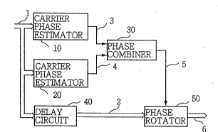
FIG. 1 is a schematic block diagram illustrating a
digital phase demodulator using the carrier recovery
system of the invention by way of its first preferred
invention;
FIG. 2 is a schematic block diagram illustrating
;,
,details of the carrier phase estimator 10 in FIG. l;
FIG. 3 is a schematic block diagram illustrating
details of the carrier phase estimator 20 in FIG. l;
¢
~ 15 FIG. 4 iS a schematic block diagram illustrating
:s details of the phase.combiner 30 in FIG. l;
, FIG. 5 is a schematic block diagram illustrating
details of the phase rotator 50 in FIG. l;
FIG. 6 is a schematic block diagram illustrating
a digital phase demodulator using the carrier recovery
.. system of the invention by way of its second preferred
:~: invention;
.~
FIG. 7 is a signal space diagram illustrating four
reference signal points of signals resulting from the
. 25 demodulation of four-phase phase-modulated signals,
: four:decision areas,.and.a set of reerence.signals
.u corresponding to one of these decision areas;
. ,.
,. .
: `
.
. .
. . , :
: :- ' : I
. ~ .
:
'
:
_ 7 - 2~2~23~
FIG. 8 is a signal space diagram illustrating eight
reference signal points of signals resulting from the
demodulation of eight-phase phase-modulated signals,
eight decision areas, and a set of reference signals
corresponding to one of these decision areas; and
FIG. 9 is a schematic block diagram illustrating
details of the carrier phase estimator 70 in FIG. 6.
DETAILED DESCRIPTION OF THE PREFERRED EMBODIMENTS
Referring to FIG. 1, a digital phase demodulator
using the carrier recovery system according to the
. present invention comprises a first carrier phase
.~ estimator 10, a second carrier phase estimator 20, a
~ phase combiner 30, a delay circuit 40 and a phase
3 rotator 50. In FIG. 1, the first and second carrier
15 phase estimators 10 and 20 and the phase combiner 30
constitute the carrier recovery system according to
`3 the invention.
A receive signal, which is a quadrature (or complex)
signal, is supplied from an input signal line 1, fed to
i 20 the phase rotator 50 by a signal line 2 via the delay ,
circuit 40, and supplied as the demodulated signal of
the quadrature signal from an output signal line 6.
:~ The first and second carrier phase estimators 10 and 20
, send their outputs over signal lines 3 and 4, respectively,
.:3 25 i-or real number signals to the phase combiner 30, whose
.:i
. .
.... .
,,, ~ ~, ,
: : , . - .
,:.: . : .
- 8 - 2 ~ ~ 2 3 ~
output is supplied to the phase rotator 50 over another
signal line 5 for real number signals. Similarly in FIG. 2
and thereafter, double lines represent paths for quadrature
signals and single line~s, paths for real number signals.
In the digital phase demodulator shown in FIG. 1,
the first carrier phase estimator 10 receives from the
input signal line 1 digital phase-modulated signals
transmitted in a Rice fading environment. The estimator 10
extracts carrier components from the received signal, and
subjects the extracted carrier component to phase averaging
operation. The averaged carrier component is supplied to
the phase combiner as a first carrier compoment. This
phase averaging operation is achieved by narrow-band
filtering. The bandwidth of this filtering is set about
equal to the noise bandwidth of the PLL in the conventional
carrier recovery system, somewhere between 1/50 and 1/200
of the modulation rate of the received signal. This
~ filtering improves the C/N ratio of the first carrier
¦ component, whose phase slip rate is significantly
reduced, too. Since this filtering achieves phase
averaging over a relatively long period of time, phase
jitters due to noise in the first carrier component
are sufficiently reduced, but the fast phase fluctuation
due to fading is also averaged. Therefore, the phase
~ .
~`. 25 of the first carrier component cannot track the fast
:i phase fluctuation due to fading.
.
:,,
, ................................... .
. .
. -.
:: . . .. . I
' ' ' ' ': . , ` '
9 2~232
Meanwhile, the second carrier phase estimator 20 also
extracts carrier component from the received signal
supplied from the input signal line 1, and subjects the
extracted carrier component to phase averaging operation.
5 The averaged carrier component is supplied to the phase
combiner 30 as a second carrier component. This operation
is achieved by wide-band filtering. The bandwidth of this
filtering is set about equal to or somewhat wider than the
maximum fading pitch. Since this filtering achieves phase
10 averaging over a relatively short period of time, the
. phase of the second carrier component tracks the fast
phase fluctuation due to fading, but jitter due to noise
; in the carrier component is relatively great.
The phase combiner 30 determines the deviation of
s 15 the phase of the second carrier component from that of
:i
the first carrier component, and adds the determined
deviation, after limiting the range of its fluctuation,
to the phase of the first carrier component. The
deviation is the phase deviation of the second carrier
component with reference to the first carrier component
whose phase is sufficiently cleared of phase fluctuation
due to noise or fading. This deviation, therefore,
contains relatively great phase jitter due to noise
and fast phase fluctuation by fading. By limiting the
.,~ ,
fluctuating range of the deviation, phase slips due to
noise-attributable phase jitters can be prevented.
~;
:,.
.~.
~,.,. ; , . ;. -, . .
~ ... .
lo- 2~25232
Consequently, the phase outputted by the phase combiner 30
can track fading-invited phase fluctuation within the
limited range of phase fluctuation, and its slip rate is
sufficiently low. What is important here is that the
fluctuating range of the deviation is limited after it
is determined. Phase slips cannot be prevented by
directly processing the second carrier component.
The delay circuit 40 delays the received signal by
the response time from the inputting of the received
signal to the first and second carrier phase estimators
10 and 20 till the phase recovery by the phase combiner 30.
The phase rotator 50 gives a phase rotation to the signal
from the delay circuit 40 by the phase of the output of
the phase combiner 30. The phase rotator 50 outputs the
~15 demodulated signal.
'jThe digital phase demodulator illustrated in FIG. 1
.~wi-ll now be described in further detail with reference
to FIGS. 2 to 5 together.
Referring to FIG. 2, the first carrier phase estimator
~,20 10 consists of an Mth-power operating circuit ll, a finite
impulse response (FIR) filter 12 and an arc tangent (tan
:
operator 13.
Signals entered into the Mth-power circuit 11 are
composed of a sampled data sequence obtained by sampling
two quadrature components of the M-phase phase-modulated
received signal at a bit timing. The Mth-power circuit 11
'
.~, ~
.: - ~ , I
.
2 3 2
removes the modulation of the input signal by multiplying
their frequency by M, the number of modulating phases for
the receivedsignal. In ~sual Mth-power operation, both
amplitude and phase are multiplied in the Mth-power. In
the present invention, the Mth-power circuit 11 multiplies
only the phase, while keeping intact the amplitude, of the
input signal and outputs the resultant phase-multiplied
signal. Therefore, if the input signals Sl(n) being
represented by:
. I .
Sl(n) = Il(n) + jQl(n) = ¦Sl(n)¦ exp ~jOl(n)~ (1)
where ¦Sl(n)¦ = ~Il(n)2 + Ql(n)2 , the output signal S2(n)
of the Mth-power circuit 11 can be represented by:
S2(n) =¦Sl(n)¦ exp {jM~l(n)} = I2(n) + iQ2(n) (2)
": ~,
.. ~, In the Mth-power operation, keeping the amplitude of the
~ 15 output signal equal to that of the input signal is intended
.,
to minimize nonlinear loss. This aspect is analyzed in
detail in the article by A.J. Viberbi et al. referred to
above.
",
~ The FIR filter 12 is a narrow-band carrier filter to
;.i 20 keep the phase slip rate low by improving the C/N of the
.:~
` carrier component, which is the output signal S2(n) of
the Mth-power circuit 11. The FIR filter 12 is composed
~: .
of a transversal filter. The number of taps of the FIR
filter 12 being represented by Nl and its tap coefficients,
...
:
: . .
:.
:
.:; .
:::
. .
.~: :
.. i , ~ , :
2~25232
by C(i) (-(Nl - 1)/2 ~ i S (Nl - 1)/2), the output signal
S3(n) of the FIR filter 12 is represented by the following
equation.
n+(Nl-1)/2
, s3(n) = ~ C(n - k)S2(k) (3)
k=n-(Nl-l)/2
At this time, the bandwidth of the FIR filter 12 is
;~, l/(NlTb), where Tb is the modulation period of received
signal, so that the bandwidth of the FIR filter 12 is
. J
set between 1/50 and 1/200 of the modulation rate l/Tb
!~ by setting the tap number Nl between 50 and 200. Further,
:;
by setting all the tap coefficients C(i) to l/Nl, the
impulse response of the FIR filter 12 becomes rectangular.
Thus, the operation load can be reduced and ideal phase
' averaging operation can be achieved.
The tan 1 operator 13 converts the output signal S3(n)
- 15 into its phase ~n(n), and outputs the converted signal to
the signal line 3 as the first carrier component.
Referring now to FIG. 3, the second carrier phase
estimator 20 consists of an Mth-power operation circuit 21,
an FIR filter 22, a delay circuit 23 and a tan 1 operator 24.
The Mth-power circuit 21 extracts carrier component
... .
~ S2(n) from the input signal Sl(n) by the same operation
i! as the Mth-power circuit 11 in ~he first carrier phase
estimator 10. Therefore, it is permissible to enter the
output signals of either one of the Mth-power circuits 11
and 21 into the FIR filters 12 and 22 and dispense with
- those of the other Mth-power circuit.
`'~'
-, ... :. ,
- 13 - 2~2~23~
The FIR filter 22 is a wide-band carrier filter to
improve the C/N of the output signal S2(n), which is
carrier component, and'tracks fast phase fluctuation due
to fading. The FIR filter 22, too, is composed of a
transversal filter. The number of taps of the FIR
filter 22, represented by N2, is so set as to make the
bandwidth l/(N2Tb) about equal to or somewhat greater
than the maximum fading pitch. If, for instance, the
maximum fading pitch is approximately 1/16 of the
modulation rate l/Tb of the received signal, the tap
number N2 is set to or slightly smaller than 16. The
impulse response of the FIR filter 22 is also made
:: .
.~ rectangular for the same reason as for the FIR filter 12,
namely, all the tap coefficients are set to l/N2.
. . .
The output signal S4(n) of the FIR fiIter 22 passes
through the delay-circuit 23 and enters into the tan 1
operator 24 which converts the input signal S4(n) into
its own phase ~w(n) and outputs the converted signal to
;~ the signal line 4 as the second carrier component. The
delay circuit 23 so adjusts the response time difference
s (Nl - N2)Tb/2 between the FIR filters 12 and 22 as to
~ make the tan 1 operators 14 and 23 output phases ~n(n)
< and Ow(n), respectively, at the same timing.
. Referring to FIG. 4, the phase combiner 30 comprises
~ 25 a frequency M-divider 31, a quadrant correction circuit 32,
x~ a subtractor 33, another frequency M-divider 34 and an
~. adder 35.
.
''`'`
.'~ '
: . - ., .
`
- 14 -
2~25232
The frequency M-divider 31 divides the phase ~ (n)
- of the first carrier component entered from the tan 1
operator 13 (Fig. 2) via the signal line 3 by the
- modulation phase number M of the received signal.- The
5 quotient is limited within the range of ~/M. The quadrant
, correction circuit 32 finds out the rotating direction of
the phase On(n) by observing the quantity of variation
3 between the phase ~n(n) and the phase ~ (n-l) which is
one symbol earlier, and expands the range of the phase
`' 10 ~n(n)/M from the frequency M-divider 31 to +~ on the
:~ basis of this rotating direction. This expansion of
the phase range can be represented by the following
equation.
:~ Hrl(n) = mod ~0 (n)/M + 2~i(n)/M, 2~ ~ (4)
:~ 15 where ~rl(n) is the phase outputted from the quadrant
correction circuit 32 after its range is expanded, and
. i(n) is represented as follows:
: ;.
, i(n) = mod {i(n-l) - sign t~n(n) ~ ~n(n~l)' 1], M }
;j if ¦~n(n) ~ ~n(n-l)¦ >
= i(n-l)
.,
Sign ~ is a function which takes the value of
+l if C~ is positive, or -1 if it is negative.
The subtractor 33 outputs the deviation of the phase
9w(n) from the phase ~n(n) by subtracting the output phase
~- . ......................... :.
: : . . , . : ~ . .
:.,: .. ~ ,: .: . : ~ , :
.. ,. . . :, ...... , -
2~252~2
~n(n) of the tan 1 operator 13 from the output phase 0 (n)
of the tan 1 operator 24 (Fig. 3), entered via the signal
; line 4. The frequency M-divider 34 divides the deviation
supplied by the subtractor 33 by the modulating phase
number M. Although the quotient is limited within the
range of +~/M, the output phase of the frequency M-divider
34 is not expanded to the range of +~ to prevent phase
slips.
The adder 35 adds the phase Orl(n) from the quadrant
correction circuit 32 and the phase from the frequency
M-divider 34. The sum ~r2(n) is:
r2 {Orl(n) +mod ~w(n) ~n(n)~ 2~.]/M, 2 ~? (5)
/
The phase Or2(n) is the carrier phase recovered from the
input signal Sl(n), and is supplied to the phase rotator 50.
Referring now to FIG. 5, the phase rotator 50 comprises
a polar-cartesian converter 51 and a complex multiplier 52.
The polar-cartesian converter 51 generates reference
carrier signals Sr2(n) in a quadrature signal form, having
~ as its phase the recovered carrier phase Or2(n) from the
;'' 20 adder 35. The complex multiplier 52 complexly multiplies
the signal Sl(n) supplied from the delay circuit 40 via
the signal line 2 and the reference carrier signal Sr2(n),
'~ and supplies demodulated signals S5(n) in a quadrature
signal form to the signal line 6. Since the response
time from the inputting of the input signal Sl(n) to the
:,~. . ; .
- 16 - 2 ~ 3 2
carrier phase estimators lO and 20 till the outputting
of the reference carrier signals Sr2(n) from the polar-
cartesian converter 51 is substantially equal to the
response time (Nl - l)Tb/2, the delay circuit 40 delays
the input signal Sl(n) by the time (Nl - l)Tb/2 but no
more so that the signal Sl(n) and the reference carrier
signal Sr2(n) be entered into the complex multiplier 52
at the same timing. Incidentally, the tan operators
13 and 24 may as well be arranged within the phase
combiner 30.
Referring to FIG.6, a digital phase demodulator which
is a second preferred embodiment of the present invention
is composed of the digital phase demodulator illustrated
in FIG. l, a decision circuit 60, a carrier phase
. . .
-~ 15 estimator 70, a delay circuit 80 and a phase rotator 90.
In the digital phase demodulator shown in FIG. 6,
., the decision circuit 60 sets decision areas where the
:x~ error rate is minimized on a complex plane, decides which
,.~
. of the decision areas the signal points of demodulated
signals S5(n) from the phase rotator 50 on the complex
~i plane are contained in. Then, the decision circuit 60
converts the demodulated signal S5(n) into reference
signal of the corresponding decision area, and outputs
the converted signal to a signal line 7. Where the
modulating phase number M is 4 for instance, the decision
circuit 60, as shown in FIG. 7, sets four decision areas
~,"
.,.,~:,. . : : : .
- 17 - 2~S ~3~
corresponding to four reference signal points (each
. represented by a black dot) of the demodulated signals
on the complex plane. If the signal point of the
demodulated signal S5(b) is, for example, in the hatched
decision area, decides that the transmitted quadrature
signal I(n) + jQ(n) is 0.707 + jO.707, which has the
greatest probability of having been transmitted among
the four rectangular signals +0.707 + 30.707, so that
the reference signal 0.707 + jO.707 is outputted. Since,
: ,s
in this instance, the area which includes the signal
points can be identified by the signs of the real number
~, and imaginary number components of the demodulated signal
S5(n). Therefore, the decision circuit 60 can be composed
of two comparators. Where the demodulating phase number M
is 8, there are eight decision areas as shown in FIG. 8.
If the signal point of the demodulated signal S5(n) is,
' for example, in the hatched decision area, the reference
! signal to be outputted is 0.924 + jO.383. In this case,
the decision circuit 60 calculates the phase of the
demodulated signal S5(n), and decides, on the basis of
the calculated phase, which decision area the signal
:,
-~ points are contained in.
Referring now to FIG. 9, the carrier phase estimator
70 consists of an inverse modulator 71, an FIR filter 72
and a tan 1 operator 73.
~ The inverse modulator 71 inversely modulates the
",,
~,
... .
.;
.,.:,
,:,,
- 18 -
` 2~5~32
. signal Sl(n) sent from the delay circuit 40 via the signal
- line 2 with the reference signal sent from the decision
circuit 60 via a signal line 7, and thereby extracts
~, carrier component. This inverse modulation is achieved
by complex multiplication of the conjugate complex signal
; of the reference signals and the signal Sl(n).
. The FIR filter 72 is a wide-band carrier filter
:.~ which improves the C/N of the carrier component from the
. inverse modulator 71 and tracks phase fluctuations due to
fading. Therefore, the bandwidth of the FIR filter 72 is
.. set about equal to that of the FIR filter 22 in the second
carrier phase estimator 20. Thus, the ~IP~ filter 72 may
have the same configuration as the FIR filter 22.
The tan~l operator 73 converts the carrier component,
~ 15 extracted by the inverse modulator 71 and subjected to
:~: phase averaging operation by the FIR filter 72, into its
own phase and outputs the converted signal to a signal
, line 9.
, Referring again to FIG. 6, the phase rotator 90,
having the same configuration as the phase rotator 50,
gives a phase rotation to the signals Sl(n), having
:. passed the delay circuits 40 and 80 and sent via a
slgnal line 8, by the output phase of the carrier phase
estimator 70. Demodulated signals are supplied from a
signal line 16, which is the output line of the phase
rotator 90. The delay circuit 80 is used for delaying
.~
' .~
~,..
,, .
:
.
: - lg - 2~2523,'
-'
the output signal of the delay circuit 40 by the time of
; the delay of carrier component by the FIR filter 72. If
the number of taps of the FIR filter 72 is N3, the delay
time will be (N3 - l)Tb/2. The tan 1 operator 73 of the
carrier phase estimator 70 and the polar-cartesian
converter (not shown) of the phase rotator 90 are used
to keep the amplitude of the output signals of the FIR
filter 72 constant. Therefore, these two circuits can
be.replaced with limiter circuits.
,;;
Now, the phase combiner 30 limits the range of the
;~J fast fluctuation of phase 0w(n) of the recovered carrier
obtained by the second carrier phase estimator 20 within
;~ +~/M. Therefore, if the fast phase fluctuation due to
', fading go beyond the range of +~/M, transient phase jumps
will occur to the recovered carrier phase ~r2(n) supplied
~ by the phase combiner 30. Reference signal obtained by
."~ demodulating the input signals Sl(n) and making decision
on the basis of the recovered carrier phase Or2(n) involving
:~i these phase jumps would be subject to errors. The C/M in
, 20 the worst fading environment conceivable in practical
. operation ranges from 7 to 10 dB, and even at this C/M
. the likely error in the reference signal is considexably
small, but not small enough to ignore. Since the inverse
modulator 71 inversely modulates the input signal Sl(n)
.. 25 with the reference signal involving errors, the carrier
component it provides contain phase jumps. However, since
: . .:
'~'. !
,`:
`'~,, . , ' ~ , .. ' " ' ' ', ' :
,.' , ' ' ' : . .':' ' ' . . . '~:: , '
- 20 - 2~2~232
,
the phase averaging operation by the FIR filter 72 smoothes
both phase jitters due to noise and phase jumps, it has
the effect to reduce the influence of phase jumps occurring
in the phase combiner 30 in the recovered carrier phase
supplied by the carrier phase estimator 70. Meanwhile,
since no such limitation of the range of fast phase
, fluctuations as what is performed in the phase combiner 30
takes place in the carrier phase estimator 70, no phase
. jumps will occur even if fast phase fluctuation due to
- 10 fading go beyond +~/M.
Therefore, the error rate of the demodulated signal
supplied by the phase rotator 90 is somewhat improved over
that of the demodulated signal obtained on the output
signal line 6 of the phase rotator 50, in other words
~ 15 the output signal of the digital phase demodulator shown
,.
~ in FIG. 1.
,.,~
As hitherto described, the present invention, by
providing first carrier recovering means for obtaining
a recovered carrier phase by averaging the phase of
carrier component, obtained by nonlinearly operating
received signal, over a relatively long period of time;
second carrier recovering means for obtaining a recovered
carrier phase by averaging the phase of carrier components,
obtained by nonlinearly operating received signals, over
.. 25 a relatively short period of time; and phase combining
`'~.' means for adding the deviation of the recovered carrier
,;,
. .
.:
:
.
:,i,.
,~,.
:
~ - 21 - 2~2~3~
phase obtained by the second carrier recovering means
; from that obtained by the first carrier recovering means
to the recovered carrier phase obtained by the first
carrier recovering means after limiting the fluctuating
range of the deviation, can restrain the slipping rate
of the recovered carrier phase and, at the same time,
improve its compliance with fast phase fluctuations.
By synchronous detection of digitally phase-modulated
received signal with the recovered carrier phase obtained
in this manner, the adaptability of synchronous detection
~, to mobile communication systems, which has been considered
less adaptabile in a fading environment, can be improved.
If the received signal is demodulated and subjected
~i to decision with the recovered carrier phase supplied by
,', 15 the phase combining means, the carrier component, which
~`J iS obtained by inversely modulating the received signal
~l with the result of decision, is averaged in phase over
a period substantially equal to the phase average by the
' second carrier recovering means, and the recovered carrier
phase thereby obtained is used for synchronous detection
of the receive signal, the error rate can be further
improved.
, Since digital operations are used for the processing
of signals in different parts of the system according to
the present invention, the invention can be realized by
; combining digital signal processors (DSP's3 available as
::,
:~,
,3~
,....
-::
....
, ............................ .
~,, . . ~. . .
- 22 -
: 2~2523~
IC's, and there can be provided a compact digital phase
demodulator requiring no adjustment and excelling in
handling ease.
, .
Although the invention has been described with refence
- 5 to specific embodiments, this description is not meant to
be construed in a limiting sense. Various modifications
of the disclosed embodiments, as well as other embodiments
of the invention, will become apparent to persons skilled
in the art upon reference to the description of the
invention. It is therefore contemplated that the appended
claims will cover any such modifications or embodiments
,
- as fall within the true scope of the invention.
.i
' -
-.:
:"
~ .;
:
:,~
~:,.,s,
-;,
, ~
,., . , ",., :.
~-.. - . . '',, '' .