Note: Descriptions are shown in the official language in which they were submitted.
202~2~
RD-19161
METHOD AND A~a~aI~i FOR PRQ~UCI~ T~E
SUpE;RCONDUCT~RS
Backaround of the Invention
l. Field of the Invention
The present invention relates to a me~hod and appa-
ratus for producing superconductors in the form of an elong-
ated tape.
2. Description of the Related Art
Although there is considerable technical and econ-
omic incentive to make superconducting magnets from A-15 type
superconductors, especially from the so-called post-Niobium-
Tin superconductors, e.g., Nb-Al, Nb-GE, Nb-Ga, this new
class of superconductors have proven to be difficult to pro-
cess into bundles of fine wire as had been the practice with
superconducting compounds previously used, such as niobium-
15 titanium. Further, attempts to date at making tape supercon- - - -
ductors of the A-15 type have been successful in producing
;~ only short lengths of tape superconductors. Splicing such
short lengths into longer, useful lengths of superconductor
tape creates serious problems with the reliability of the
conductor.
Perhaps the most common processes to date for form-
~: lng A-15 type superconducting materials are plasma spray
forming and the melt spinning. The former has the disadvan-
tage that the conductors must be formed in relatively thick - ~ -~
sectlons in order,to ensure continuity of the superconductor
material and of its superconductive properties. The melt
spinning process has the disadvantage that there is a limita-
tion on the amount of material which can be molten and
ejected out under pressure to form a thin film on a sub-
strate. The process is therefore not believed to be well
2~2~2~
RD-19161
suited for large scale production of superconductor products.
Chemical vapor deposition (CVD) could be employed as well,
but this process is slow and costly and also would not be
well suited for large scale production.
Other processes disclosed in the art include form-
ing a bulk "tape" of the superconducting material and heating
and melting a center part of the tape such that the melted
and resolidified section forms a compound superconductor
region on the tape. The process has at least one disadvan-
tage in that a much larger amount of the base material is
required than is actually converted to the superconductive
material. A further process disclosed in the art calls for
forming a substrate of one of the elements of the compound
superconductor and applying to the substrate a coating of a
second element of the compound, heat treating the coated sub-
strate to produce intermetallic compounds, and subsequently
irradiating the coated substrate with a high-energy density
beam such as an electron beam or laser beam. The process has
the disadvantage that numerous process steps are required
before the superconducting material is produced. Because
both of these processes involve preparing a substrate for
later processing, the processes will generally only be useful
in producing superconductors of some finite length. Still
other methods proposed in the art have similar drawbacks and
provide further evidence of the difficulties in producing
superconductor products using A-15 type compound superconduc-
tors.
It is therefore a principal object of the present
invention to provide a simplified method for producing long
lengths of superconductor tape.
It is another object of the present invention to
provide a method for producing a superconductive tape of an
--2--
,-.,- :' : ~ ' ~ . . .: .
RD-19161
A-lS type compound superconductor suitable for use in super-
conductor magnets.
It is a further object of the present invention to
provide a method for substantially continuous production of
S superconductive tape products of indeterminate length.
It is yet a further object of the present invention
to provide a method for producing superconductor tape prod-
ucts which is especially well suited for on-line dimensional
control and quality control of the tape product.
It i5 a further object of the present invention to
provide an apparatus for producing elongated tape supercon-
ductors at speeds suitable for large scale production.
Summary of the Invention
The above and other objects of the present inven-
tion are achieved in a method involving continuously melting
the end of a wire feedstock made of a compound superconductor
material, thereby forming a molten bead of the material at
the tip of ~he wire, and passing a cooled tape substrate or
backing material into contact with the molten bead to wipe
the molten material onto the substrate. The wire feedstock
20 is continuously advanced as the end is melted and wiped onto - -
the substrate, and a film of the molten superconductor com-
pound material is formed and resolidifies on e tape sub-
strate, thus forming a superconductive tape product.
Laser heating of the wire feedstock is preferably
employed to produce the molten bead at the end of the wire,
although alternative approaches can be employed, such as gen-
eratlng an arc at the tlp of a pair of wires in a manner sim-
ilar to an arc welding process.
The process of the present invention may also be
performed as a two step process, wherein a first film of one
2 ~ ;3 L~
RD-19161
of the elements of the compound superconductor is laid down
on the substrate and the second element is laid down on top
of the first film. The thickness and continuity of the
deposited films can be monitored and controlled using a laser
tracking system. The tape may then optionally be heated to
induce a diffusion reaction between the films of the two ele-
ments to produce the superconductor, either "on-line" with a
subsequen~ heating device, or ~off-line~ at a later point in
time.
The apparatus according to the present invention
includes a means for melting a tip of the wire to produce a
molten bead, a means for transporting a tape substrate of
extended length in a predetermined direction with respect to
the molten bead and into contact with the molten bead to wipe
molten material from the bead onto the substrate-to form a
film of superconductor material, a means for continuously `
~feeding the wire toward the substrate to me melted to replace
molten material wiped from the bead, and a means for cooling
the film to solidify the superconducting material.
B~i~f Descri~tion of the Drawin~s
These and other features of the of the present
invention and the attendant advantages will be readily appar-
ent to those having ordinary skill in the art and the inven-
tion will be more easily understood from the following
detailed descriptlon of the preferred em~odiments of the pre-
2S sent invention taken in conjunction with the accompanying
drawings wherein like reference characters represent like
parts throughout the several views, and wherein:
FIG. 1 is a side view of an apparatus used in prac-
ticing the method of producing a tape superconductor in
accordance with a preferred embodiment of the present inven-
tion;
2~2~25~
RD-19161
FIG. 2 is a side view of an apparatus used in prac-
ticing an alternate preferred version of the method of the
present invention;
FIG. 3 is a substantially schematic representation
of an alternate apparatus which may be used in practicing the
method of the present invention;
FIG. 4 is a further substantially schematic repre-
sentation of an alternate apparatus which may be used in
practicing the method of the present invention.
~ LLL~ DESCRIPTION OF THE INVENTION
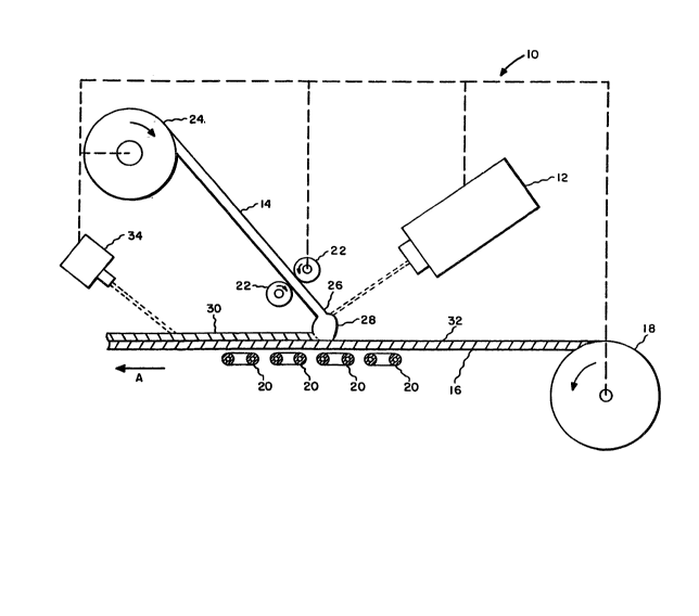
Referring initially to FIG. 1, an apparatus 10 for
producing tape superconductors according to the method of the
present invention is depicted. A high powered laser heat
source 12 of a type known generally in the art is positioned
such that the laser beam is directed at the tip of a wire 14
which, in this embodiment, is made up of the superconductor
compound material. The apparatus and method of the present
invention are particularly well suited for use with A-15 type
superconductors, e.g. Nb-Al, Nb-Ge, Nb-Ga and Nb-Sn, although
other superconductor materials may be employed in producing
tape superconductors.
One potentially significant advantage found in the
method of the present invention is that the method may be
carried out without the necessity of employing a vacuum cham-
ber or otherwise drawing a vacuum in any part of the process.
It is expected that the method will preferably be carried out
in a controlled air or inert gas environment, either of which
provides relative simplicity of operation as compared to the
use of a vacuum chamber which other of the known processes
employ.
--5--
- 2a~2~
RD-19161
A cooled substrate or backing material 16, such as
copper, is disposed to pass in close proximity to the tip of
the superconductor wire 14 when the substrate is moved hori-
zontally and axially in a direction along a longitudinal axis
of the apparatus, as indicated by arrow A, past the tip of
the wire. ~he tape substrate may be supplied in any conven-
tional manner, shown in FIG. 1 as being unwound from supply
roll 18. The cooling of the substrate may be accomplished in
a conventional manner, by passing the substrate through a
refrigeration unit or chill rolls ahead of the point where
the superconductor wire 14 is located, or may be cooled from
underneath by colls 20, as depicted substantially schemati-
cally in FIG. 1. Substrate 16 is chilled in order to prevent
the possibility that the substrate will melt when the film is
deposited thereon, and also to effect a rapid quench and
solidification of the film, and therefore the means for
chilling the substrate is preferably designed to chill the
substrate both immediately before the molten material is
deposited, and immediately thereafter.
The superconductor wire 14 is continuously fed in a
direction toward substrate 16, passing between roller guides
22 at a location above the substrate and above the tip area
of the wire irradiated by the laser beam, in order to support
the wire and maintain the position of the wire tip at a sub-
stantially con-~tant location. The wire feed system may be of
a type used in consumable electrode arc welding processes,
indicated substantially schematically by spool 24 from which
the wire is fed. Roller guides 22 and/or spool 24 may be
driven in order to feed the wire toward the substrate.
In this preferred embodiment of the method of the
present invention, the laser heat source 12 directs a laser
beam with substantial power at the tip 26 of the superconduc-
tor wire 14, which melts the wire material to form a molten
bead 28 of the superconducting material. A suitable laser
;:
~2XJ?'~
RD-19161
source could be a commercially available C02 laser with a
power output capability which, depending upon several factors
including the speed at which the process is carried out,
would be about 50W minimum to about lOOOW maximum. The sub-
strate 16 is positioned to be in contact with this moltenbead 28, and as the substrate is moved laterally with respect
to the bead, molten material is wiped onto the substrate to
form a superconductor film 30 on a top surface 32 of the
substrate 16. The Apeed of tra~el of the substrate and of
lO the wire feed are preferably coordinated such that the wire -
14 is continuously fed toward the substrate and melted by the
laser heat source to continuously replenish the molten bead,
with the bead formed at the tip of the wire being wiped onto
the substrate to produce a continuous film of a predetermined
lS thickness. Stated another way, it is preferred in the pres-
ent apparatus and method to maintain the molten bead at a
substantially constant volume as the process takes place.
The thickness of the deposited film may preferably range from
about l/2 mil to about 2 mils, although other thicknesses may
prove to be suitable in various applications.
Because the substrate is cooled in this preferred
embodiment, the molten superconductor material is quickly
quen~hed and solidified once the material exits the area
heated by laser 12. The finished product, comprising the
substrate and the superconductive film disposed thereon can
be made in long, substantially continuous lengths, the length
being theoretlcally limited only by the length of the tape
substrate starter material and/or the upper limit of the
length of a wire feedstock which can be continuously supplied
by the wire feed system.
The upper surface 32 of the tape substrate 16 may
optionally be treated in order to improve the wettability of
the ~ubstrate which will have the effect of improving the
bonding of the superconductive film thereto. Examples of
_7_
such treatments would be an acid cleaning of the surface or
other treatments to remove oxides therefrom, or a physical
roughening of the surface.
The method of the present invention lends itself
well to on-line control, whether automatic or manual, in
obtaining a tape having desired dimensions, especially a
thickness dimension, and also having a desired level of
deposit continuity and quality. A laser tracking system,
shown schematically at 34, similar in pertinent respect to
arc bead laser tracking system previously developed for use
in arc welding processes, is especially well suited for moni-
toring and controlling the thickness and deposit continuity
(quality) of the superconductor material deposited on the
tape. It will be readily recognized that both the wire feed
rate and the speed of travel of the substrate could be var
ied, as well as the melting of the wire, in controlling the
thickness of the deposited film. Increasing the speed of
travel of the tape substrate would have a tendency to result
in a thinner superconductive film layer, as would a reduction
in the wire ~eed rate and in the melting of the wire. Con-
versely, a decrease in e speed of travel of the tape sub-
strate or an increase in the wire feed rate (assuming that
the laser has sufficient power to completely melt the tip of
the wire at such a rate) would tend to have the effect of
increasing the resulting thickness of the superconductive
film.
As indicated previously, a preferred thickness for
the deposited material may be selected in a range from about
1/2 mil to 2 mils. The laser trackin~ system 34 will thus
preferably contain process control hardware and/or software
and will preferably be operati~ely coupled to the various
components responsible for the substrate supply rate, the
wire feed rate and the power output of the laser heat source,
as indicated by broken lines in FIG. 1. Other monitoring and
. ;
--8--
2~2~2~4
RD-19161
control means previously employed in the art may be used in
performing these functions as well.
FIG. 2 depicts an apparatu.s 100 which may be
employed to perform the method described above, or, where
S desired, a variation of that method. Except where indicated
to the contrary, the components depicted in FIG. 2 will
preferably have the same operating characteristics as the
analogous components depicted and described with respect to
Claim 1. The apparatus in this embodiment comprises a first
and a second laser heat source 102, 104, respectively, of a
type known generally in the art. The laser heat sources 102,
104 are spaced apart from one another with respect to an
axial direction of travel A of tape substrate 106. The first
laser heat source is positioned to direct a laser beam at the
tip 108 of a first wire 110 made up of a first element from
which the compound superconductor is to be formed.
The second laser heat source 104 is positioned
"downstream" of first laser heat source 102, the downstream
direction being determined by the direction of travel A of
the substrate. The second laser heat source is positioned to
direct a laser beam at the tip 112 of a second wire 114 made
up of a second element from which the compound superconductor
is to be ~ormed.
The tape substrate or backing material 106 is
preferably cooled in a manner similar to the FIG. 1 embodi-
ment, and is disposed to pass in close proximity to the tips
108, 112 of the first and second superconductor wires 110,
114, when the substrate is moved horizontally, as indicated
by arrow A, past the tips of the wires. As in the FIG. 1
embodlment, substrate 106 may be supplied from a supply roll
116, or other conventional means, and the cooling of the sub-
strate can be accomplished through the use of cooling coils
118.
br
2~2~2~
- RD-19161
The first wire llO is continuously fed in a direc-
tion toward substrate 106, passing between roller guides 120
at a location above the substrate and above the tip area of
the wire which is to be irradiated by the laser beam. The
5 roller guides are provided in order to support the wire and
maintain the position of the wire tip at a substantially con-
stant location. The wire feed system, represented by spool
i22, may be of a type used in conventional arc welding pro-
cesses as discussed above with respect to FIG. l.
The first laser heat source 102 directs a high
energy las~r beam at the tip 108 of the first wire 110, which
heats and melts the wire material, thus forming first molten
bead 124. As in the FIG. 1 apparatus, substrate 106 is posi-
tioned to be in contact with the molten bead 124, and as the
15 substrate is moved laterally with respect to me bead, molten
material from the bead is continuously wiped from the wire
onto substrate 106 to form a first film 126 on the upper sur-
face 107 of the substrate, in a manner substantially identi-
cal to the method in FIG. 1.
The second wire 114 is continuously fed toward sub-
strate l06, pass ng between roller guides 128 at a location
above the substrate 106 and first deposited film 126 and
above the tip area of the wire which is to be irradiated by
the second laser beam. The wire feed system which his
25 preferably identical to that previously described, is repre-
sented by spool 130.
The second laser heat source 104 directs a high
energy laser beam at the tip of 112 of second wire 114, which
heats and melts the wire material, thus forming second molten
30 bead 132. Molten material from the second molten bead is
contlnuously wiped from the wire onto the first film 126,
which forms a second film layer 134 disposed on top of first
film 126.
--10--
2~2~
--~ RD-19161
The two wires llO, 114, and thus the two film lay-
ers 126, 134, in this embodiment preferably comprise the two
elements from which the compound superconductor is formed.
For example, in producing a niobium-tin compound superconduc-
tor, the first wire used to lay down the first film 126 maycompris~ niobium (Nb), and the second wire, forming second
film 134, would comprise tin (Sn~. Superconductive proper-
ties are attained in such a structure by diffusion of a suf-
ficient quantity of the tin into the niobium such that an
Nb3Sn (A-15 type) phase is formed. In this "two step" pro-
cess described with reqpect to FIG. 2, it may be possible to
achieve an adequate level of diffusion without further pro-
cessing, particularly if the second film is deposited in its
molten state on a first film which has not been fully
quenched.
While it is generally recognized that, in order to
obtain adequate levels of diffusion with the materials of
interest herein, the materials must be held at a minimum tem-
perature at least one-half of the melting temperature of the
material having the higher melting temperature. In the tape
superconductor described as an example above, i.e., a nio-
bium-tin superconductor on a copper backing or substrate, the
diffusion must take place at a temperature lower than one-
half of the melting temperature of niobium ~2700 C~, as the
copper would melt at that temperature. However, a sufficient
amount of diffusion may be obtained by slowing the quench
rate of the first film 126 deposited on the substrate, and by
holding the temperature for a slightly longer time period.
Alternatively, if it is desired to augment the dif-
fusion occurring at the time the second film is deposited, afurther reaction between the films may be carried out "on-
line" by a further heating device, such as a plasma arc torch
136, of a type known generally in the art. In the example
above, the torch 136 may preferably be designed to heat the
'3 2 ~ ~
RD-19161
tape to approximately 900 C, which is roughly 15~ cooler than
the melting temperature of the copper substrate. The temper-
ature and duration of additional heating can be selected to
ensure adequate diffusion of the tin into the niobium, as
indicated schematically in FIG. 2 showing a single supercon-
ductor film 138 disposed on substrate 106 resulting from the
heating and diffusion, even thougb in reality a complete dif-
fusion of the element is not likely to be actually achieved.
The further reaction, where necessary or desirable, may
optionally be conducted "off-line", as is done in other pro-
cesses known in the art.
It is to be recognized that the above method may be
practiced with any of the other A-15 type compound supercon-
ductors or other compound superconductors in a similar man-
ner. Likewise, the order in which the films are deposited isnot believed to be critical to the method, and therefore the
secondary element (e.g., Ga, Ge, Al, Sn) may be deposited at
the first film, with the niobium being deposited as the sec-
ond film.
As with the "one-step" process described with
respect to FIG. 1, the thickness and continuity of the films
deposited on the tape substrate 106 can be monitored and con-
trolled using a laser tracking system operatively coupled
with the tape substrate and wire feed speed controls.
FIG. 3 depicts, in substantially schematic form, an
alternative apparatus 200 for producing tape superconductors
according to the method of the present invention. This appa-
ratus 200 employs a different means for generating a molten
bead o~ material than those depicted in FIGS. 1 and 2. In
this embodiment, an arc is created at the tips of a first and
a second superconductor wire 202, 204, respectively, which
are fed to a predetermined location immediately above the
moving substrate 206.
-12-
2~2~2~
RD-19161
:
As in FIGS. 1 and 2, the direction of movement of
the substrate is indicated by arrow A, and the substrate 206
may be supplied by any conventional means including a supply
roll as depicted in either FIG. 1 or FIG. 2. The first and
second wires 202, 204 are likewise continuously supplied in a
conventional manner such as a wire spool like those depicted
in FIGS. 1 and 2.
In this embodiment, a first and second pair of
roller guides 208, 210, associated with the first and second
wires 202, 204, act not only to feed and guide the wires to
the desired location, but also preferably serve as electrodes
to feed current through the wires in a manner similar to con-
ventional DC arc welding process. A conventional DC arc
power supply 212 is connected to each of these pairs of
roller guides 208, 210, to provide a current running through
each of the first and second wires.
The first and second wires 202, 204 are both fed to
the same predetermined location, and an arc is struck between
the tips 214, 216 of the current-carrying wires, thereby
forming a molten bead 218 comprising material melted from the
tips of each of the two wires. The moving substrate 206 is
positioned, as in FIG. 1 to come into contact with the molten
bead 218, and to wipe molten material onto an upper surface
220 of the substrate to form a film 222 which is subsequently
quenched to form an elongated superconductive film or tape on
tape substrate 206.
.
The moving substrate 206 is preferably cooled or
chilled (cooling means not shown) in a manner similar to the
substrates of FIGS. 1 and 2, in order to prevent possible
melting of the substrate and to promote a rapid quench of the
deposited film. In addltion, the FIG. 3 apparatus further
include~ a means for delivering a cooling gas at the upper
side of the molten bead 218 formed in the method described
2 ~ 2 .~ 2 ~ ~
RD-19161
above. The cooling gas may be delivered through schema~i-
cally depicted conventional tubing 224, in line with one or
more valves 226 provided, as necessary, to control the flow
rate of the cooling gas or to completely shut off the flow of
cooling gas in instances where in is not desired. The flow
of cooling gas may improve the process and the quality of the
film deposits and tape superconductors produced in that the
cooling gas will force the molten bead 218 downwardly toward
the substrate, and in addition will assist in quenching the
deposited film 222.
The first and second wires 202, 204 are preferably
each made of the desired superconductor compound material,
whether of the A-15 type or other superconductor composi-
tions. Alternatively, it may be possible to employ as wire
feedstock a first wire 202 comprising a first element of the
compound superconductor and a second wire 204 comprising the
second element of the compound superconductor. For example,
a niobium wire and an aluminum wire may be used in the pro- -
cess as first and second wires 202, 204, respectively, and
the superconductive compound phase Nb3Al would have an oppor-
tunity form in solution in the molten bead and subsequently
be deposited on the substrate 206.
FIG 3 also depicts a plasma arc torch 228 located
downstream of the area in which the molten bead is deposited
on the substrate to form film 222. The plasma arc torch is
employed, as in FIG. 2, to heat the deposited film to promote
the diffuslon of the elements comprisin~ the compound super-
conductor. This further heating of the film may not be nec-
essary in all instances as adequate diffusion of the elements
may be achieved at the time the film is depo~ited and before
the deposited film 222 has been quenched. Also, it would be
possible, if further diffusion of the elements is desired, to
carry out an "off-line" diffusion reaction process in lieu of
the "on-line" process represented by plasma arc torch 228.
-14-
i: :
2~2~
- RD-19161
FIG. 4 depicts, in substantially schematic form, a
further alternative apparatus 300 for producing tape super-
conductors according to the method of the present invention.
The apparatus in this Figure is used to perform a "two-step"
film deposition process similar in many respects to the pro-
cess described with respect to FIG. 2. For example, the wire
feed means and the substrate supply means may preferably be
of the same type as those previously described.
In this embodiment, an arc is struck between a
first pair of continuously fed first and second wires 302,
304, at the wire tips 303, 305, forming first molten bead
306, which is wiped onto an upper surface 308 of moving tape
substrate 310. Downstream of the formation of first film
312, an arc is struck between a second pair of continuously
fed first and second wires 314, 316, at the wire tips 315,
317, forming second molten bead 318, which is wiped onto an
upper surface 320 of first film 312, thus forming second film
322. ~-
The means for striking the arcs in the FIG. 4
embodiment may preferably be similar to that described with
respect to FIG. 3. A first and second pair of roller guides
324, 326 is provided to guide the first pair of first and
second wires 302, 304, to the desired predetermined position
above substrate 310, and the roller guides 324, 326 are cou-
pled to a first DC arc power supply 328, and serve as elec-
trodes for delivering current through the wire to create the
arc. An additional or second pair of first and second roller
guides 330, 332 is provided to guide the second pair of first
and second wires 314, 316 to the desired predetermined posi-
tion above first film 312, and the roller guides 330, 332 arecoupled to a second DC arc power supply 334, and serve as
electrodes for delivering current through the wire to create
the arc. Although not shown in FIG. 9, it is to be under-
stood that a cooling gas may preferably be delivered blowing
L~ ~
---` 2~2~
RD-19161
downwardly on each of first and second molten beads 306, 318,
in a manner identical to that described with respect to FIG.
3.
In an example in which this embodiment is employed
5 to produce an A-15 type compound superconductor the first -
pair of first and second wires 302, 304 may comprise niobium
or a basic alloy containing niobium, and each of the second
pair of first and second wires 314, 316 may preferably com-
prise the second element (Al, Ga, Ge, Sn) or an alloy of the
second element and niobium. The film deposition process it-
self may, under appropriate circumstances, provide adequate
diffusion of the elements in the first and second films in
order to produce the compound superconductive material. How-
ever, as with the embodiments discussed with respect to FIGs.
1-3, an "on-line~ or ~off-line" heating of the tape and
deposited films to produce further diffusion of the elements
may be employed where desired or if required.
It is to be understood and recognized that the
foregoing detailed description of the invention is given
merely by way of illustration, and many modifications and
variations will be apparent to those skilled in the art with-
out departing from the spirit or scope of the present inven-
tion. Therefore, the scope of the invention is to be deter-
mined by reference to the appended claims.
-16-