Note: Descriptions are shown in the official language in which they were submitted.
--` 2025632
1 27879-39
FIELD OF THE INVENTION
The present invention generally relates to routing
methods and routing systems, and more particularly to a routing
method and a routing system for a switching system having a
pluralit,y of paths.
BRIEF DESCRIPTION OF THE DRAWINGS
., Figure 1 is a system block diagram showing an example of
:.
a conventional ATM switching system having SRMs connected in a
, plurality of stages;
, 10 Figure 2 is a system block diagram for explaining a
conventional routing system;
Figure 3 is a system block diagram for explaining an
operating principle of the present invention;
Figure 4 is a system block diagram showing a first
embodiment of a routing system according to the present invention;
~ Figure 5 is a system block diagram showing an embodiment
:' of a converter of the first embodiment shown in Figure 4;
Figure 6 is a system block diagram showing an embodiment
of an output module of the first embodiment shown in Figure 4;
~. 20 Figures 7A and 7B are diagrams respectively showing
'~s3 formats of a cell and a tag;
~3 Figures 8A and 8B are cell timing charts for explaining
.~:
~ an operation of the first embodlment;
.: Figure 9 shows an operation sequence of the first
. embodiment;
. Figure 10 is a diagram for explaining a VPI/VCI table of
the converter;
Figure 11 is a diagram for explaining a VPI/VCI table of
.
.
:, . . -
,
.. ,,. . .. : .
2025632
2 27879-39
the output module;
Figure 12 is a system block diagram showing an
embodiment of a converter of a second embodiment of the routing
system according to the present invention;
Figure 13 is a system block diagram showing an
embodiment of an output module of the second embodiment;
Figure 14 is a flow chart for explaining an operation of
a cell and tag generation controller within the converter shown in
Figure 12;
Figure 15 is a flow chart for explaining an operation of
a control circuit within the output module shown in Figure 13;
Figures 16A and 168 are cell timing charts for
explaining an operation of the second embodiment; and
Figure 17 shows an operation sequence of the second
embodiment.
8ACKGROUND OF THE INVENTION
In order to freely transfer files at a high speed, it is
.
~ necessary to use a high-speed broadband communication network. In
.;,~,
;~ such a communication network, the communication band must be
several tens of Mbits/s or greater which is extremely large
compared to a communication band for telephones and data
communications which i# in the range of 64 kbits/s x n. Recently,
there is active research in this field of broadband communication,
and the asynchronous transfer mode (ATM) communication ls regarded
as an effective method of communication.
The ATM communication technique is proposed in
Kawarasaki et al., "Perspective of ATM Communication Technique, -
Evolution of 8roadband Communication Network", Journal of
.~,
,
~ A
. ~ . . .
.,~. ... . . . .
, .~ . . -
-~ 2025632
3 27879-39
Electronic Information Communication Society, Vol. 71, No. 8,
August 1988, pp. 806-814. According to the ATM communication,
digitized information such as audio, data and video information
are divided into blocks which have a fixed length and are called
cells. The ATM is a label multiplexing in which each cell is
transmitted with a destination information which is added to a
header of the cell and a channel is identified from a label within
the header. In the ATM, the occurrence of the cells is based on
; an information transmission request and is asynchronous. Hence,
¢ 10 the ATM is different from a synchronous transfer mode (STM) which
; is a time position multiplexing in which a channel is identified
from a time position of a time slot within a frame. In the STM,
~ the time slot occurs periodically regardless of the existence of
,~ information transmission.
".~
The ATM transmits the information after converting the
information into a unified format, that is, cells. The header of
the cell must include channel identification, routing information
and the like. The routing information indicates which route is to
be taken within an ATM switching system. The ATM switching system
directs the cell to a desired output port by selecting connections
of each of unit switches based on the routing information which is
added to the header of the cell.
Figure 1 shows an example of an ATM switching system
having 3 stages of self routing modules (SRMs), where each SRM has
N input links and N output links. For example, a route within the
ATM switching system is swltched during communication, and Flgure
1 shows a case where a route "a" indicated by a one-dot chain line
is switched to a route "b" indicated by a phantom line. When a
:
,.,~,
~:
` 1`'' ' ', . ~ ' ' ' ', ' , ' , ', '
:'.' , ' ' ' ' , ' ' . :
`` 2025632
4 27879-39
fault occurs in a certain route or a congestion occurs in a local
part within the switching system, it is necessary to swltch the
route to a route which still has margin in its capacity. The
congestion is caused by an inappropriate call accept control logic
and when a user inputs a number of cells exceeding a declared
value, and in the latter case, the cells input exceeding the
declared value are disposed, for example.
When the route is simply switched, the cell which is
transferred through the new route after the switching of the route
may go ahead of the cell which is transferred through the old
route before the switching of the route. In other words, since
the new route after the switching of the route is free compared to
the old route, the cell sequence is dlsordered at the output end
of the ATM swltching system. When the cell sequence is
disordered, lt is no longer possible to carry out a positive
signal processing. Hence, when switching the route, it is
necessary to take measures to prevent the cell which is
transferred through the new roùte after the switching of the route
~ from golng ahead of the cell which ls transferred through the old
:~ 20 route before the swltchlng of the route.
.,;,
Conventlonally, vlrtual channel identification (VCI)
; converters 21 and 22 shown in Figure 2 which are provlded in a
tage precedlng an ATM swltchlng system 1 havlng the structure
shown in Flgure 1 have bufferlng functlons so as to prevent the
cell which is transferred through the new route after the
switchlng of the route from golng ahead of the cell whlch i~
: transferred through the old route before the switching of the
-` route.
,~ ,
~: . .. : . . ~
2025632
5 27879-39
Each cell has a VCI number added to an ATM header
thereof, and cells having various VCI numbers are transmitted time
sequentially. A VCI discriminator 3 shown in Flgure 2
discriminates the VCI number of each cell, and a reference is made
' to a VCI table 4 so as to obtaln via selectors 5a and 5b those
cells having the VCI numbers which are to be processed. In other
-~i words, when a route switching instruction is received from a
, central processing unit (CPU) 6, those cells which have
. predetermined VCI numbers and are to take the new route within the
~ 10 ATM switching system 1 are temporarily stored in a first-in-first-
: out (FIF0) memory 7 by the switching of the selectors 5a and 5b,
3 while those cells which are to take the old route within the ATM
,~i
switching system 1 are passed as they are by the switching of the
~, selectors 5a and 5b. The cells which are to take the new route
:1 and are stored in the FIF0 memory 7 are read out after a
.,
predetermined time which is preset by a timer 8. This
. predetermined time corresponds t,o a maximum tolerable delay time
within the ATM switching system 1 such that the cell which is
transferred through the new route after the switching of the route
is prevented from going ahead of the cell which is transferred
~; through the old route before the switching of the route.
:'
~ When switching the route ln the conventional system
. .: .
shown in Figure 2, the cells which are to take the new route
within the ATM switching system 1 are temporarily stored in the
VCI converter 22 which is provided in the stage preceding the ATM
switching system 1 and are read out and input to the ATM switching
system 1 after the predetermined time which is preset by the timer
8 within the VCI converter 22. In other words, the cells which
~`
.~v'.
.~ I
~.~'.'' ,. ...
.. ~ . , , :.:~
. .
; - . .
2025632
6 27879-39
,:
~ are to take the new route must wait before being subjected to the
., switching process in the ATM switching system 1. For this reason,
~' a long delay time is introduced between the cells having the
various V~I numbers, and there is a problem in that a subse~uent
~ signal processing cannot be carried out efficiently within a short
;: time because of the delay introduced at the input stage of the ATM
,~ ~
switching system 1.
~ SUMMARY OF THE INVENTION
,. Accordingly, it is a general object of the present 10 invention to provide a novel and useful routing method and routing
system in which the problems described above are eliminated.
~. Another and more specific object of the present
; invention is to provide a routing method for routing cells which
are transferred through one of a plurality of paths within a
asynchronous transfer mode switching system selected by routing
information, where each of the cells include a header and an
information field and the routing method comprises the steps of
adding first routing information to incoming cells at an input
stage of the asynchronous transfer mode switching system when
supplying the cells to the asynchronous transfer mode switching
; system, generating a route switching confirmation cell in response
to a route switching instruction and for adding second routing
information to incoming cells thereafter so as to supply the route
switching confirmation cell and the cells added with the second
routing information to the asynchronous transfer mode switching
system, where the second routing information is different from the
first routing information and is determined by the route switching
instruction, comparing routing information of the cells with the
-- 2025632
. 7 27879-39
. second routing information at an output stage of the asynchronous
. . .
transfer mode switching system in response to the route switching
instruction, outputting each cell from the asynchronous transfer
mode switching system having routing information different from
the second routing information as it is, and temporarily storing
each cell from the asynchronous transfer mode switching system
having routing information identical to the second routing
information and reading out and outputting the stored cell after
the route switching information cell is output from the
asynchronous transfer mode switching system. According to the
routing method of the present invention, it is possible to prevent
a long delay tlme from occurring between the cells, and
accordingly carry out a subsequent signal processing efficiently
within a short time.
Still another object of the present invention is to
.;,
. provide a routing system for routing cells which are transferred
. ,~. .
~ through one of a plurality of paths within an asynchronous
~ transfer mode switching æystem selected by routing information,
,,,~
where each of the cells include a header and an information field
and the routing system comprises a converter part coupled to an
;~. input stage of the asynchronous transfer mode switching system and
~ including first means for adding first routing lnformation to
j. lncoming cells when supplylng the cells to the asynchronous
-........... transfer mode switching system and second means for generating a
~ route switching confirmation cell in response to a route switching
:~:
`. instruction and for adding second routing information to incomlng
........... cells thereafter so as to supply the route switching confirmation
. . ~
'.4' cell and the cells added with the second routing information to
. . .
2025632
7a 27879-39
the asynchronous transfer mocle switching system, where the second
routing information is different from the first routing
information and is determined by the route switching instructlon,
and an output module part coupled to an output stage of the
asynchronous transfer mode switching system including third means
for comparing routing information of the cells with the second
routing information in response to the route switching
instruction, fourth means for outputting each cell from the
asynchronous transfer mode switching system having routing
information different from the second routing information as it is
and fifth means for temporarily storing each cell from the
asynchronous transfer mode switching system having routing
information identlcal to the second routing information and
readlng out and outputting the stored cell after the route
switching confirmation cell is output from the asynchronous
transfer mode switching system. According to the routing system
of the present invention, it is possible to prevent a long delay
time from occurring between the cells, and accordingly carry out a
. .,
subsequent signal processing efficiently within a short time.
Other objects and further features of the present
:.~. invention will be apparent from the following detailed description
:~.; when read in conjunction with the accompanying drawlngs.
;~ DESCRIPTION OF THE PREFERRED EMBODIMENTS
.,:1
;;
; .,
~,:
~ .
2025632
8 --
.,
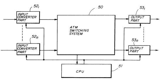
1 First, a description will be given of an
operating principle of the present invention, by
referring to FIG.3. In FIG.3, an ATM switching system
50 includes a plurality of SRMs which are connected in a
plurality of stages so that a switching of the route is
possible. A CPU 51 controls the entire system shown in
FIG.3. Input converter parts 521 through 52n are
provided in a stage preceding the ATM switching system
50 and normally add normal routing information to
incoming cells. When a route switching instruction is
received from the CPU 51, the input converter part 52i
generates a route switching confirmation cell and adds
to the incoming cells thereafter new routing information
which is determined by the route switching information,
where i = 1, ..., n. Output parts 531 through 53n
are provided in a stage subsequent to the ATM switching
- system 50. The output part 53i rewrites an internal
table to the new routing information in response to the
route switching instruction from the CPU 51 and compares
the routing information added to the incoming cells with
~ the new routing information written in the table. When
i the routing information added to the incoming cell
$ differs from the new routing information written in the
table, the output part 53i outputs the incoming cell
as it is. On the other hand, when the routing
~; information added to the incoming cell matches the new
routing information written in the table, the output
part 53i temporarily stores the incoming cell in a
; memory and reads out and outputs this cell from the
memory after the route switching confirmation cell is
received.
Therefore, the basic operation of the present
invention can be summarized as follows. That is, the
input converter part 52i adds the route switching
confirmation cell to the incoming cells when the route
switching instruction is received from the CPU 51, and
the input converter part 52i outputs the incoming
....
. . .
. .,
,.,
,.,. : ~
32
g
,. ,
1 cells thereafter by adding thereto the new routing
information. The ATM switching system 50 detects the
routing information of the cells received from the input
converter part 52i, and carries out the switching
process by switching the links of SRMs based on the
detected routing information. The output part 53i
rewrites the table to the new routing information and
compares the routing information of the incoming cells
with the new routing information written in the table.
When the routing information of the incoming cell
differs from the new routing information, it is judged
that the incoming cell took the old route and the output
part 53i outputs the incoming cell as it is. On the
other hand, when the routing information of the incoming
cell matches the new routing information written in the
table, it is judged that the incoming cell took the new
route and the output part 53i temporarily stores the
incoming cell in the memory and reads out and outputs
this cell from the memory after the route switching
'! 20 confirmation cell is received and output.
` In the ATM switching system 50, the new route
is free, and thus, the cell which takes the new route
may go ahead of the cell which takes the old route. For
this reason, the present invention temporarily stores
the cell which takes the new route within the ATM
switching system 50 before outputting the same to the
output link, so as to prevent the cell which takes the
; new route from going ahead of the cell which takes the
` old route. The cell which takes the new route within
the ATM switching system 50 is corrected by storing this
cell in the memory of the output part 53i which is
` provided in the stage subsequent to the ATM switching
` system 50. Hence, compared to the conventional system
which stores the cell which is to take the new route for
the predetermined time at the stage preceding the ATM
switching system, the present invention does not
:,
~ introduce the long delay time between the cells and it
.,,
:.~.
.,
,~.
.
~2~32
-- 10 --
1 is possible to efficiently carry out the subsequent
signal processing within a short time.
Next, a description will be given of a first
embodiment of the routing system according to the
~, 5 present invention, by referring to FIG.4. The routing
j system shown in FIG.4 includes an ATM switching system
~, 10, a VPI/VCI converter part 11, an output module (OM)
part 12 and a CPU 13, where VPI stands for "virtual path
identifier" and VCI stands for "virtual channel
identifier". The ATM switching system 10 includes 2 x 2
SRMs #1 through #6 which are arranged in 3 stages. The
VPI/VCI converter part 11 is provided in a stage
preceding the ATM switching system lO and is made up of
converters #o through #3 respectively having a structure
shown in FIG.5. The output module part 12 is provided
in a stage subsequent to the ATM switching system lO and
is made up of output modules #0 through #3 respectively
having a structure shown in FIG.6. The CPU 13 controls
the VPI/VCI converter part 11 and the output module part
12 as will be described later.
~ Input links #0 through #3 and output links #0
- through #3 shown in FIG.4 are lines for transferring
~ cells which have a cell format shown in FIG.7A. Lines
'~ from output ends of the converters #0 through #3 to
input ends of the output modules #0 through #3 transfer
tags which have a tag format shown in FIG.7B. As shown
, in FIG.7A, each cell has an ATM header and an
information field, and the ATM header includes a head
check field, a spare field and a VPI/VCI field. On the
other hand, as shown in FIG.7B, the tag includes a cell
~ identification field CIP, routing information fields X,
;~l Y and Z for respectively indicating routing information
~i of the SRMs in the first through third stages, and a
~3 don't care field. The cell identification field CIP
: 35 indicates the kind of cell, that is, whether the cell is
a normal cell (CIP = O) or a route switching
;~ confirmation cell (CIP = 1). Hence, the tag is a kind
~s;~3
.
."
., ,
~. ` . .. .`.. ,. .-. . :; ~ .
';I.,: ' ' :. :'
;.` .` ,. ~. ~ ` .
,~, . . . . . .
i.,`...... - , ` ~ , .
.. . . ... : .
;. : . ~ .. . -
... .,. ,, ` .
- - 2 ~ 3 2
-- 11 --
1 of routing information.
A virtual channel is identified by the VPI and
. the VCI. But for the sake of convenience, it is assumed
in this embodiment that the virtual channel is
:~ 5 identified by the VCI alone to simplify the
description. In actual practice, however, the virtual
~ channel is identified by the VPI and the VCI or by the
-- VPI alone, and the VPI may be fixed in the case where
the virtual channel is identified by the VPI and the
VCI. The terms VPI and VCI are defined by CCITT
standards.
Next, a description will be given of a case
where an old route within the ATM switching system 10 is
switched to a new route by taking as an example a cell
which has a VCI number VCI = OOOO(H) at the input link,
with reference to FIGS.5, 6, 8 and 9. The old route
:~ includes the converter #0, the SRM #1, the link O of the
: SRM #1, the SRM #3, the link O of the SRM #3, the SRM
#5, the link 0 of the SRM #5, and the output module #O
.; 20 in FIG.4. On the other hand, the new link includes the
.. 1 converter #0, the SRM #1, the link 1 of the SRM #1, the
SRM #4, the link 0 of the SRM #4, the SRM #5, the link 0
of the SRM #5, and the output module #O in FIG.4.
. FIGS.8A and 8B are cell timing charts, and FIG.9 shows
;, 25 an operation sequence.
: When a cell #O having the VCI number VCI =
OOOO(H) shown in FIG.8A is input to the converter #0, a
VPI/VCI discriminator part 33 shown in FIG.5
discriminates the VCI number and refers to a VPI/VCI
:. 30 table 32 shown in FIG.10 to look up a corresponding VCI
: number VCI = FFFF(H) on the output link of the converter
,.i,`~ #0. A selector 35 adds a VCI number VCI = FFFF(H) to
~, the header of a cell #l the timing of which is adjusted
.~ by a delay circuit 34. As shown in FIG.10, the VPI/VCI
.. i 35 table 32 stores the VPI/VCI number and the tag
information (kind of cell and routing information) on
the output link of the converter #0 in correspondence
j
, .
. ~ , .
:: , , ... ,, , ..
.: , ~ ~ . : - .. ; :- ..
: l
- 12 -
: 1 with the VPI/VCI number on the input link of the
converter #0. The tag information which indicates the
kind of cell (0) indicating normal cell and the routing
, information (000) read from the VPI/VCI table 32, and
5 the cell and the tag indicated by ~ in FIG.8A are
obtained in a step 100 shown in FIG.9 by switching
,A selectors 36 and 37 by a cell and tag generation
controller 31. The cell and the tag are obtained in a
: step 101 shown in FIG.9 by an operation similar to the
10 above when the cell #1 having the VCI number VCI =
- OOOO(H) is input to the converter #0.
An operation similar to the above is also
carried out when a cell #2 having another VCI number is
input to the converter #0, and the cell and the tag
15 indicated by ~ in FIG.8A are obtained.
When the SRM #3 shown in FIG.4 generates a
' congestion when processing the cell #2, the CPU 13
: decides to switch the route of the cell which has the
s VCI number OOOO(H) on the input link of the converter #0
20 in order to reduce the load on the SRM #3.
The CPU 13 notifies the output module #0 to
;. change the routing information of the cell having the
VCI number VCI = FFFF(H) (VCI = OOOO(H) at the input
`~ link of the converter #0 becomes VCI = FFFF(H) at the
output link of the converter #0) from "000" (X = 0, Y =
0, Z = 0) to "100" (X = 1, Y = 0, Z = 0) in a step 102
.~ shown in FIG.9. A control circuit 20 of the output
module #0 shown in FIG.6 assigns a FIF0 memory 211 in
response to a route switching instruction from the CPU
30 13 which is received via an interface (I/F) 29, and
rewrites the VPI/VCI table 22. The state of the cell
having the VCI number VCI = FFFF(H) is rewritten from
`:' the "normal state" (00) to a "swi~ching state" (01), and
in addition, the routing information is rewritten from
(000) to (100). As shown in FIG.ll, the routing
information and the cell state information are set for
every VPI/VCI number in the VPI/VCI table 22.
.c,~
., ,: . :. ...................... ..
"
- 13 - ~2~2
1 On the other hand, the CPU 13 instructs the
converter #0 via an interface (I/F) 39 to switch the
route of the cell having the VCI number VCI = OOOO(H) on
the input link of the converter #0 in a step 103 shown
in FIG.9. A control circuit 30 of the converter #0
shown in FIG.5 notifies the VCI number VCI = OOOO(H),
the old routing information (000) before the switching
and the new routing information (100) after the
switching to the cell and tag generation controller 31
in response to the route switching instruction which is
obtained from the CPU 13 via the interface 39. In this
state, the VPI/VCI discriminator part 33 shown in FIG.5
detects the incoming cell #2 shown in FIG.8A and having
the VCI number which is "empty", assuming that the cell
#3 is an empty cell following the cell #2. The empty
cell refers to a cell in which the VPI/VCI number is
"empty", that is, a cell which is not used for transfer
of information. Hence, the cell and tag generation
controller 31 outputs a signal which indicates the kind
of cell (1) in the tag, that is, the route switching
confirmation cell. By the switching of the selectors 36
;; and 37, the cell indicated by ~ in FIG.8A having the
VCI number VCI = FFFF(H), the tag indicating the kind of
cell ~1) which is the route switching confirmation cell,
and the routing information (000) are obtained in a step
; 104 shown in FIG.9. Thereafter, the cell and tag
~,,! generation controller 31 rewrites routing information of
the VPI/VCI table 32 corresponding to VCI = FFFF(H) on
~; the output link of the converter #O to the new routing
information (100) in a step 105 shown in FIG.9.
When a cell #4 shown in FIG.8A having the VCI
~, number VCI = OOOO(H) is received following the cell #3,
the new routing information (100) is obtained from the
VPI/VCI table 32 because the routing information is
already rewritten to the new routing information (100).
By the switching of the selectors 36 and 37, the cell
indicated by ~ in FIG.8A and the tag are obtained in
.:
;,.' -- ' . _
... ~ . .
~ '`' t ~3 ~
- - 14 -
1 a step 106 shown in FIG.9. For a cell #5 and the cells
which follow, the cells having the VCI number VCI =
OOOO(H) are obtained with a format similar to that of
the cell #4. Since the cells #2 and #5 have VCI numbers
different from VCI = OOOO(H), these cells #2 and #5 pass
through the converter #0 but are not supplied to the
output module #0.
- The cells #0, #1, ... which are obtained from
the converter #0 are subjected to the switching process
in the ATM switching system 10 shown in FIG.4 and pass a
route dependent on the routing information. But since
. ~ . .
the new route (100) is free, it is assumed that a cell
which takes the new route goes ahead of a cell which
takes the old route as shown in FIG.8B. A description
will be given of the operation of the output module #0
in this case.
. .s
~s In FIG.8B, it is assumed that the cell #0
which takes the old route, the cell #4 which takes the
new route, the cell #1 which takes the old route, a cell
#2' which is input to the output module #0 but is
uncertain of the converter from which this cell
originates, and the cell #3 which takes the old route
are obtained at the input link of the output module #0.
In this case, the cell #4 which takes the new route goes
~ 25 ahead of the cells #1, #2' and #3 which take the old
- route. The cell #0 shown in FIG.8B is obtained from the
old route in the step 100 shown in FIG.9. The VCI
number VCI = FFFF(H) of this cell #0 is detected in a
. VPI/VCI and tag detector 23 shown in FIG.6, and the
; 30 VPI/VCI and the tag (routing information) are supplied
to the control circuit 20 for comparison with the
~;;' routing information and the state information which are
s'~ obtained from the VPI/VCI table 22. The state
;~ information of the VPI/VCI table 22 is already rewritten
to the "switching state" (01) by the route switching
i, instruction from the CPU 13 which is obtained via the
interface 29. In this case, the routing information
:,...
j,,:
: ...
.: :~
~:::, . . ' :
. ........ ~ .
:......... ., ~ ; :. , .: .
.,.~: . ., :~ : : ;
.-:....... :.: ,
- 15 -
1 (000) of the cell #0 and the routing information (100)
from the VPI/VCI table 22 differ~ Hence, a switch 24
and a selector 25 are switched by a control of the
control circuit 20 so that the cell #0 which is obtained
via the detector 23 is not stored in the FIF0 memory
211 but is output as it is to the output link of the
output module #0 in a step 107 shown in FIG.9 and
indicated by ~ in FIG.8B.
Next, when the cell #4 is received at the
: . 10 input link of the output module #0 in the step 106 shown
in FIG.9, the comparison of the routing information is
made in the control circuit 20 by a procedure similar to
the procedure described above. In this case, because
the cell #4 is obtained from the new route, the routing
. 15 information thereof is (100). Hence, the routing
~'J' information (100) of the cell #4 and the routing
information (100) of the VPI/VCI table 22 are the same.
In addition, the state information of the VPI/VCI table
.i 22 is the "switching state" ~01). Therefore, the cell
. 20 #4 is stored in the FIF0 memory 211 by switching the
:.................... switch 24 by the control of the control circuit 20 in astep 108 shown in FIG.9. In this state, an empty cell
~:i
. is output on the output link of the output module #0 as
indicated by ~ in FIG.8B. If there exists a cell
~: 25 which has the same routing information (100) as the cell
; #4, this cell is also stored in the same FIF0 memory
.~ ,. .
Next, when the cell #1 is received at the
~ input link of the output module #0, this cell #1 is
$. 30 output to the output link of the output module #0 as it
~; is by the switching of the switch 24 and the selector 25
. in a step 109 shown in FIG.9 as indicated by ~ in
.~ FIG.8B, similarly as in the case of the cell #0 because
.~ the cell #1 also takes the old route. The next cell #2
.~` 35 is also output to the output link of the output module
#0 as it is as indicated by ~ in FIG.8B, similarly
as in the case of the cells #0 and #1.
,. ~,:
..:,
:..
:
. . . : :: : :.~ -
..... ., ~ .. :.. - --. .
2:
-- 16 --
:'
:
1 When the cell #3 (route switching confirmation
cell) is received at the input link of the output module
#0 in the step 104 shown in FIG.9, the detector 23
detects this route switching confirmation cell #3 and
the control circuit 20 instructs a read with respect to
the FIF0 memory 211 and also switches the selector
25. Accordingly, the cell #4 which is stored in the
FIF0 memory 211 is read out and output to the output
link in a step 110 shown in FIG.9 as indicated by
in FIG.8B. At the same time, the control circuit 20
rewrites the state information of the VPI/VCI table 22
from the "switching state" (01) to the "sweep-out state"
(11). When the FIF0 memory 211 becomes empty by the
read out, the control circuit 20 rewrites the state
.15 information of the VPI/VCI table 22 to the "normal
state" (00), and the normal cells which are thereafter
received via the new route described by the routing
information (loo) are output as they are in a step 111
:~shown in FIG.9. If there exists a cell other than the
..20 cell #4 which is stored in the FIFO memory 211, this
cell is output to the output link of the output module
#0 under the control of the detector 23 which detects
the empty cell shown in FIG.8B and the control circuit
20 which switch the selector 25.
Although the cell #4 which takes the new route
~, goes ahead of the cell which takes the old route and the
~;~ cells #0, #4, #1, #2' and #3 are received at the input
link of the output module #0 in this sequence, the cells
~:~ are obtained with the correct sequence at the output
link of the output module #0 as indicated by ~
through ~ in FIG.8B. The correct sequence is formed
by the cell #1 having the VCI number VCI = FFFF(H), the
.~ empty cell which is a cell from another converter, the
~ cell #l having the VCI number VCI = FFFF(H), the cell
~35 #2' which is a cell with a different VCI number, and the
~cell #4 which is obtained in place of the empty cell
~,#3. In this case, no long delay time is introduced
. i
. ...
:.
.:
,, i .~ . .
... .
:, , : :~,;, . ... ..
.. , . ~ : . - :. ~ ;
2~7,~1~32
.
- 17 -
1 between the cells as in the conventional system which
stores the cells which are to take the new route for the
predetermined time at the input end of the ATM switching
system. Therefore, the subsequent signal processing can
be carried out efficiently within a short time according
to this embodiment.
Next, a description will be given of a second
embodiment of the routing system according to the
present invention. In this second embodiment, the block
lo system shown in FIG.4 is also used. However, the
converters #0 through #3 of the VPI/VCI converter part
11 respectively have a structure shown in FIG.12, and
the output modules #0 through #3 of the output module
part 12 respectively have a structure shown in FIG.13.
lS In FIG.12, those parts which are the same as those
corresponding parts in FIG.5 are designated by the same
reference numerals, and a description thereof will be
omitted. In FIG.13, those parts which are the same as
those corresponding parts in FIG.6 are designated by the
~ 20 same reference numerals, and a description thereof will
- be omitted. In addition, for the sake of convenience,
it is assumed that cells similar to those described in
conjunction with the first embodiment are input to the
, converter #0 and output to the output module #0.
In FIG.12, the discrimination result of the
VPI/VCI discriminator 33 indicative of the VPI/VCI is
`~ also supplied to a cell and tag generation controller
31A. In addition, a signal indicative of a cell timing
is supplied to the cell and tag generation controller
31A.
In FIG.13, a signal EMP indicative of the
, empty cell is supplied from the VPI/VCI and tag detector
. 23 to a control circuit 20A. In addition, the cell
;i which is supplied to the VPI/VCI and tag detector 23 is
also supplied to the control circuit 20A.
In the first embodiment, the cell
identification field CIP of the tag shown in FIG.7B is
,
..,.~,
.,;"
;.... - .
i.,
,., i~; . , :, .~. ;
.
~2~2
-- 18 --
1 made up of 1 bit to indicate the normal cell when CIP =
0 and the route switching confirmation cell when CIP =
1. However, in this second embodiment, the cell
identification field CIP of the tag is made up of 2
bits. The normal cell is indicated by CIP = 00, the
route switching confirmation cell which is an empty cell
is indicated by CIP = 10, and the route switching
confirmation cell which is a normal cell is indicated by
` CIP = 11. CIP = 01 indicates a don't care.
FIG.14 shows an embodiment of an operation of
i the cell and tag generation controller 31A shown in
FIG.12 when switching the route. When a route switching
instruction is received from the CPU 13 via the
interface 39 in a step S1, a step S2 judges whether or
not the timing corresponds to the header of the cell
based on the signal which indicates the cell timing.
When the judgement result in the step S2 becomes YES, a
step S3 judges whether or not the cell is an empty
~ cell. When the judgement result in the step S3 is NO, a
;~ 20 step S4 judges whether or not the VCI number VCI = AAAA,
where A denotes a variable. A step S5 carries out a
normal process of controlling the selectors 36 and 37 to
output the cell and the tag input to the converter #0,
and the process ends.
;l 25 On the other hand, when the judgement result
in the step S4 is YES, a step S6 controls the selector
37 to output the tag of the old route and outputs the
cell identification field CIP = 11. Then, a step S7
~ supplies a rewrite instruction to the VPI/VCI table 32
x~ 30 to rewrite the VPI/VCI table 32, and the process ends.
When the judgement result in the step S3 is
YES, a step S8 inserts VCI = AAAA into the VCI number,
outputs the tag of the old route, and outputs the cell
identification field CIP = 10. After the step S8, the
, 35 process advances to the step S7.
FIG.15 shows an embodiment of an operation of
the control circuit 20A shown in FIG.13. When a cell is
. .
.,
::. , ... ., ............... :,
,-.~: , . . .- :.
. .: . . .:. - .. . ~ . .
. . : : : ,.. : .
.: . . . .
~Q~
- 19 -
1 received in a step Sll, a step S12 judges whether or not
the cell is an empty cell. When the judgement result in
the step S12 is NO, a step Sl3 judges whether or not the
state of the cell is the ~switching state" (ol), the
"normal state" (oo), or the "sweep-out state" (11).
When the "normal state" (oo) is detected in
the step S13, a step S14 controls the selector 25 to
pass the cell as it is, and the process ends.
- When the "switching state" (01) is detected in
the step S13, a step S15 judges whether or not the cell
is obtained through the old route. The process advances
to a step S22 which will be described later when the
judgement result in the step S15 is NO. A step S16
judges whether or not the cell is a route switching
confirmation cell when the judgement result in the step
S15 is YES. The process advances to the step S14 when
the judgement result in the step S16 is NO. On the
other hand, when the judgement result in the step S16 is
YES, a step S17 judges whether or not a cell is stored
in the assigned FIFO memory 21i, for example. A step
;~ S18 changes the state to the "sweep-out state" when the
judgement result in the step S17 is YES, and a step Sl9
changes the state to the "normal state" when the
judgement result in the step S17 is NO. After the step
~.~
S18 or S19, a step S20 judges whether or not the cell is
;~ an empty cell. The process advances to a step S25 which
will be described later when the judgement result in the
step S20 is YES. But when the judgement result in the
step S20 is NO, a step S21 passes the cell as it is and
~ii 30 the process ends.
On the other hand, when the step S13 detects
;~ the "sweep-out state", the step S22 stores the cell into
: .
~A the assigned FIFO memory 21i, for example, and the
process advances to the step S25.
The step S25 judges whether or not a cell is
stored in the assigned FIFO memory 21i, for example.
The process ends when the judgement result in the step
.,
, ~ .
.,
".: ~ . j .
.: , , .
~2~3~
- 20 -
1 S25 is NO. On the other hand, when the judgement result
in the step S25 is YES, a step S26 carries out a routine
for determining the output cell. A step S27 outputs the
cell from the FIFO memory 21i, for example, based on
the routine carried out in the step S26. A step S28
judges whether or not there still exists a cell in the
FIFO memory 21i, for example. The process ends when
the judgement result in the step S28 is YES. On the
other hand, when the judgement result in the step S28 is
NO, a step S29 rewrites the state information of the V~I
which is assigned to the FIFO memory 21i to the
"normal state" and the process ends.
Therefore, in this second embodiment, the cell
timings at the input and output stages of the ATM
switching system 10 respectively become as shown in
FIGS.16A and 16B. In FIGS.16A and 16B, the same
designations are used as in FIGS.8A and 8B, and a
description thereof will be omitted. In this second
embodiment, it is assumed that the cell #3 has the VCI
number VCI = 0000 at the input link of the converter #0
as shown in FIG.16A. The cell identification field CIP
of the cells at the output link of the converter #0 is
indicated as shown in FIG.16A.
As shown in FIG.16B, the cell #3 is output to
,~ 25 the output link of the output module #0 as it is, and
;3 the outputting of the cell #4 from the output module #0
'~ waits until the cell #3 is output to the output link of
the output module #0 and an empty cell is input to the
input link of the output module #0. In other words,
unlike the first embodiment which outputs the cell #4 in
place of the cell #3, the cell #3 is output as it is and
the outputting of the cell #4 waits until the empty cell
; is received in a step 150 shown in FIG.17. FIG.17 shows
an operation sequence of the second embodiment. In
FIG.17, the same designations are used as in FIG.9, and
a description thereof will be omitted.
Of course, as a modification of the second
.,.
,
,,
. . .
: . : . :: :
: , .
: :
~2~63~
- 21 -
1 embodiment, the outputting of the cell #4 may wait until
a cell having a VPI/VCI number corresponding to that of
- the cell #4 is received.
Moreover, as another modification of the
second embodiment, the outputting of the cell #4 may
; wait until the empty cell is received or the cell having
the VPI/VCI number corresponding to that of the cell #4
- is received, whichever occurs first.
Further, the present invention is not limited
to these embodiments, but various variations and
. modifications may be made without departing from the
scope of the present invention.
:~
.,
't;
~' 25
.:
r:
..
::?
;~ 30
.. . .
,, .
~ 35
~ .
...;
i .
" .
.
., . -~ . . I
. - ~
. - ., . , : ~ ~ -
~ . . - .
... , . , ... . . .