Note: Descriptions are shown in the official language in which they were submitted.
2~2~
METHOD AND APPARATUS FOR
BAUD TIMING RECOVERY
Technical Field
The present invention relates to clock synchronization
circuits and, in particular, describes a method and apparatus for
locking local baud timing to remote baud timing.
Background of the Invention
In order to properly recover the data contained in a
received signal a data communications receiver, such as a modem,
must synchronize its baud clock with the baud clock of the remote
transmitter. Typically, the clock in the local device and the clock in
the remote device will both be crystal controlled and therefore the
local baud clock and the remote baud clock, even without a
2s synchronization circuit, typically differ less than 0.02 percent in
frequency. However, even with this small offset in frequency, the
cumulative phase difference between the two baud clocks
eventually becomes large enough to cause errors in the data
transfer.
Modern modems use an analog-to-digital (A/D)
converter to periodically sample the received analog signal and
conve~t it to a digital format to provide a sampled, digitized signal,
and one or more microprocessors to process the digitized signal
and recover the data being transferred. Two types of sampling
clocks for the A/D converters are used: a variable frequency
^ g ~
sampling clock; and a fixed frequency sampling clock. When a
variable frequency sampling clock is used the recovered baud clock
is used to adjust the frequency and/or phase of the sampling clock so
that the sampling frequency, when divided by the appropriate
number ~typically an integer), yields the baud frequency and causes
the local baud clock to be locked on to the remote baud clock.
Fractionally spaced adaptive equalizers can readily
compensate for timing-phase variations between the remote
transmitter baud clock and the receiver baud clock. When there is a
0 frequency difference between these clocks the equalizer
compensates for the accumulated timing-phase difference by
shifting the equalizer tap weights in the appropriate direction along
the delay line. The spatial distribution of the equalizer coefficients
can be used to adjust the receiver sampling frequencies so that the
ls local and remote baud clocks are synchronized. The common
envelope-derived timing recovery system is replaced with a closed-
loop center-tap tracking algorithm. The receiver is locked to the
transmitter in a close~-loop manner by observing the distribution
of the equalizer tap weights. The receiver sampling clock is then
adjusted so as to maintain the dominant tap weights in the center of
the equalizer. However, in order to obtain the desired frequency
and/or phase resolution for the sampling clock, a very high
frequency master clock is typically used in conjunction with a
programmable divider chain which provides the sampling clock.
2s Typically, this divider chain and/or the sampling clock are used to
generate other clocks used by the modem. Therefore, adjusting the
frequency and/or phase of the sampling clock frequently requires
that additional steps be taken to prevent or compensate for changes
in frequency of these other clocks.
With a fixed sampling clock frequency the sampled,
digitized signal is interpolated to a high sampling rate and then
decimated down to the signal processing rate under the control of a
timing function. The timing function determines which of the
interpolated samples correspond to the optimal sampling points and
3S are to be used. An envelope-derived timing recovery system is
2~2~ ~
typically used with this technique. However, the envelope-derived
timing recovery technique can be plagued by considerable timing
jitter, especially when the channel bandwidth is fully used by a
narrow roll-off system or when the channel is severely attenuated
at the band edge.
Therefore, there is a need for a baud timing recovery
scheme which provides for the use of a fixed frequency for the
sampling clock but does not use envelope-derived timing recovery.
There is also a need for a baud timing recovery
scheme which uses a fractionally spaced adaptive equalizer to lock
the local receiver baud timing to the remote transmitter baud
timing without having to adjust the frequency of the sampling
clock.
1S Summary of the Invention
The present invention provides a method and
apparatus for baud timing recovery using a fixed sampling
frequency in conjunction with a dominate tap tracking algorithm.
More particularly described, the present invention provides a
method and apparatus for locking the baud timing of a local
receiver to the baud tirning of a remote transmitter by using a fixed
sampling frequency, a plurality of interpolating filters which
provide selectable delays to compensate for frequency differences,
a fractionally spaced adaptive equalizer to compensate for phase
differences, and a filter control circuit which controls the selection
of the interpolating filter which is in use at a particular instant, adds
or deletes samples so as to provide the proper number of samples
per baud to the adaptive equalizer, and controls of the frequency of
the bit clock.
Briefly summarized, the present invention uses a fixed
sampling clock to obtain samples of a received signal, an
interpolating filter to provide a selected delay, a fractionally spaced
adaptive equalizer which provides a set of complex coefficients,
and a control circuit for deterrnining the location of the dominant
filter tap and for cycling through the bank of interpolating filters at
the rate necessary to keep the dominant tap from moving and
eventually "falling of~' the adaptive equalizer. The control circuit
inspects the ~llter coefficients provided by the adaptive equalizer to
determine the dominant filter tap position, determines whether the
S dominant filter tap position is moving or is stationary, and adjusts
the rate of cycling through the interpolating filter so as to cause the
dominant filter tap position to remain stationary. The control
circuit also adds a sample or discards a sample, as appropriate and
at an appropriate time, so that the correct number of samples per
0 baud will be provided to the adaptive equalizer.
More particularly described, the present invention
provides for determining the difference between a preferred
dominant filter tap position and the current dominant filter tap
position, integrates this difference, and uses this integrated
lS difference to periodically update a filter pointer. The filter pointer
designates which of the interpolating filters is to be used at a
particular time. If the clocks in the remote transmitter and the
clocks in the local receiver have precisely the same frequency then,
once an interpolating filter is selected, that filter will remain
selected. However, these clocks usually differ, even though by a
small amount, and this causes the filter pointer to cycle through the
bank of interpolating filters at a rate necessary to compensate for
the frequency difference. The larger the difference in frequency
the more rapid will be the rate at which the filter pointer cycles
through the bank of interpolating filters. Typically, the rate at
which the filter pointer cycles through the bank of filters is made
during initial handshaking between the remote device and the local
device and, once determined, the rate will generally remain
constant.
The present invention applies a sum-of-the-squares
technique to the filter coefficients provided by the adaptive
equalizer in order to locate the dominate filter tap. The dominate
filter tap, by definition, will have the largest sum-of-the-squares.
The current dominant filter tap position is compared with a stored
(preferred) dominant filter tap position. If the stored value is
2 ~
greater than the current value then the stored value is used to update
the filter pointer. However, if the current value is greater than the
stored value then the current value is used to update the filter
pointer and is also stored so as to become the stored value for futu~e
S comparisons.
The difference between the current dominant filter tap
position and the stored dominant filter tap position is integrated so
that even small errors between the clock rates are compensated for.
Furthermore, the integrated signal is used to update a filter pointer
10 register whose contents indicate the appropriate interpolating filter
to be used. The integrated signal is added to the least significant bits
of the filter pointer register and the filter pointer designation is
obtained from a predetermined number of the most significant bits
of the filter pointer register. This assures that the integrated signal
15 does not cause the filter pointer to change so quickly as to cause data
errors or break the synchronization between the remote and local
clocks. However, the inte8rated signal, when repetitively added to
the contents of the filter pointer register, will cause the filter
pointer to change from designating one interpolating filter to
20 designating a next interpolating filter.
At some point the interpolating filters will rollover
from providing maximum delay to providing minimum delay.
This rollover condition indicates that the sampling frequency is
incorrect and that the cumulative error in the sampling frequency
2s has caused an incorrect number of samples per baud to be taken.
Therefore, a sample is skipped or an additional sarnple is used, so
that the correct number of samples per baud is always passed to the
adaptive equalizer. Because the sample clock frequency is fixed
adding or skipping a sample causes the local baud timing to change
30 so as to be resynchronized to the remote baud timing. However, the
number of bits per baud provided to the other receiver circuitry
(decoders, descramblers, etc.) needs to remain constant.
Therefore, the bit clock frequency is adjusted whenever the baud
timing is adjusted so that the correct number of bit clock pulses per
35 baud is always provided.
T~erefore the present invention seeks to
provide a method and apparatus for recovering baud timing by
using a fixed frequency for the sampling clock and by using
interpolating filters to compensate for the difference between the
s local clock and the remote clock.
Further the present invention seeks to
provide a method and apparatus for recovering baud timing by
using a bank of interpolating filters to prevent movement of the
dominant filter tap position of a fractionally spaced adaptive
10 equalizer.
The present invention further seeks to
provide a method and apparatus which uses the filter coefficients of
an adaptive equalizer to determine the location of and any
movement of the dominant tap in the adaptive equalizer and adjust
15 the rate at which a pointer cycles through a bank of interpolating
~llters so as to compensate for the frequency difference between the
remote clocks and the local clocks and thereby fix the position of
the dominant tap.
Still further the present invention seeks to
20 synchronize local baud timing to remote baud timing by varying
the decimation rate so that a fixed number of samples per baud is
provided to the adaptive equalizer when the number of samples per
baud before decimation is variable.
Further the present invention seeks to
2s provide a bit clock which- is synchronized to the local baud timing
and proYides a fixed number of bit clock pulses per baud
independent of the actual duration of a baud.
In one claimed aspect, the invention
provides an improved baud timing recovery circuit for
30 synchronizing a local baud timing to a recovery baud
timing. The receiver for use with a data
communications receiver comprises an analog-to-
digital converter responsive to a sample clock signal
having a fixed frequency for sampling a received
35 signal to provide a sampled received signal, a data
demodulator responsive to the sampled received signal
A for providing a received baseband data signal and an
6A
adapt:ive equalizer for providing a set of complex adaptive
equalizer filter coefficients in response to an interpolated data
signal, the received signal having a remote baud timing
established by a remote transmitter and the received baseband
data signal having a local baud timing established by the data
communications receiver. The improved baud timlng recovery
circuit for synchronizing the local baud timing to the remote
baud timing, comprises interpolating filter means responsive to
the received baseband data signal and a filter selection signal
for providing the interpolated data signal to the adaptive
equalizer and dominant tap locator means responsive to the set of
complex adaptive equalizer filter coefficients from the adaptive
equalizer for providing a dominant filter tap position signal.
Preferred dominant tap locator means is responsive to the
dominant filter tap position signal for providing a preferred
dominant tap location signal and summing means is responsive to
the dominant filter tap position signal and the preferred
dominant tap location signal for providing a difference signal.
Integrator means is responsive to the difference signal for
providing an integrated signal and filter control means,
responsive to the integrated signal and to the sample clock
signal provides the local baud timing and the filter selection
signal.
In another claimed aspect the invention provides a
method for providing local baud timing for a data communications
receiver from baud timing contained in a received signal provided
by a remote transmitter, comprising the steps of providing a
sampled received signal by sampling the received signal at points
determined by a sample clock signal having a fixed frequency,
providing a received baseband data signal by demodulating the
sampled received signal, providing an interpolated data signal in
response to the received baseband data signal and a filter
selection signal, providing a set of complex adaptive equalizer
filter coefficients in response to the interpolated data signal,
providing a dominant filter tap position signal in response to
the set of complex adaptive equalizer filter coefficients,
providing a preferred dominant tap location signal in response to
6B
the dominant filter tap position signal, providing a difference
signal in response to the dominant filter tap positon signal and
the preferred dominant tap location signal, providing an
integrated signal in response to the difference signal and
providing the filter selection signal and the local baud timing
in response to the integrated signal and the sample clock signal.
Still another claimed aspect of the invention provides
an apparatus for synchronizing local baud timing in the data
communications receiver to the remote baud timing, the data
communications receiver receiving an incoming signal provided by
a remote transmitter and the incoming signal containing a remote
baud timing established by the remote transmitter. The apparatus
comprises clock means for providing a sample clock signal,
conversion means responsive to the sample clock signal for
converting the incoming signal into a demodulated signal, delay
means for providing a set of predetermined delays and responsive
to a delay selection signal for providing a delayed signal by
delaying the demodulated signal by a selected one of the
predetermined delays, equalization means responsive to the
delayed signal for providing an equalized signal to the data
communications receiver and for providing a set of equalization
coefficients and control means responsive to the equalization
coefficients and the sample clock signal for providing the local
baud timing and for synchronizing the local baud timing to the
remote baud timing by adjusting a cycle rate at which the delay
selection signal cycles through the set of predetermined delays.
Still further the invention provides a synchronizing
method for use with a data communications receiver for receiving
an incoming signal provided by a remote transmitter, the incoming
signal containing a remote baud timing established by the remote
transmitter. More particularly the method pertains to
synchronizing local baud timing in the data communications
receiver to the remote baud timing, comprising the steps of
converting the incoming signal into a demodulated signal,
providing a set of predetermined delays, delaying the demodulated
signal by a selected one of the predetermined delays to provide a
delayed signal, cycling through the set of predetermined delays
A
at a selectable cycle rate, providing an equalized signal to the
data communications receiver and providing a set of equalization
coefficients responsive to the delayed signal and synchronizing
the local baud timing to the remote baud timing by adjusting the
selectable cycle rate.
Brief Description of the Drawing
Figure 1 is a block diagram of the preferred embodiment
of the present invention in its preferred environment.
Figure 2 is a diagram of the preferred dominant tap
locator 34 of the present invention.
Figure 3 is a diagram of the integrator and filter
pointer.
. . ,
~A
~5~
Figure 4 is a flow chart which illustrates the functions
performed by the interpolating filters and the filter control.
~ Consisting of Figs . 4A & 4B )
Figure S is a diagram of the bit clock circuit and the
5 relevant part of the master clock circuit. (Consisting of Figs.SA& 5B)
Figure 6 is a timing diagram for the signals used to
generate the bit clock.
Detailed Description
Turn now to the drawing, in which like numerals
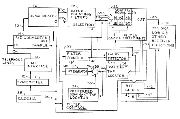
represent like components throughout the several figures. Figure 1
is a block diagram of the preferred embodiment of the present
invention in its preferred environment. The preferred
environment of the present invention is in a data communications
15 device, such as a modem. A telephone line is cormected to a line
interface 10. Line interface 10 is connected to modem transmitter
11 via conductor 12. Line interface 10 accepts signals from modem
transmitter 11 and places these outgoing signals on the telephone
line. Line interface 10 also separates incoming signals on the
20 telephone line and provides them to A/D converter 14 via
conductor 13. It should be understood that a linet such as line 13, is
representative of any signal path and is referred to as a conductor
or a bus simply for convenience. Converter 14 samples the
incoming signal on conductor 13, digitizes the signal, and provides
25 the sampled, digitized signal to demodulator 16 over conductor lS.
Demodulator 16 converts the sampled signal on conductor 15 into a
received baseband data signal having inphase (I) and quadrature
(Q) components. In the preferred embodiment, demodulator 16 is
a Hilbert transform demodulator, although other types of
3 o demodulators can be used provided that they provide the
appropriate I and Q outputs. The I and Q outputs of demodulator
16 are connected by conductors 17A and 17B, respectively, to the
inputs of interpolating filters 20. Interpolating filters 20 represents
a bank of 32 delay lines, each delay line having a different delay. In
35 the preferred embodiment, each part (I,Q) of interpolating filters
20 is implemented by an 8-stage shift register which is clocked at
2 ~
the sampling frequency. The set of eight outputs (one from each
stage) is multiplied by a set of eight coefficients and the resulting
products are summed to provide the interpolated output signal.
There are 32 sets of coefficients, so 32 different filters can be
s simulated. The 32 filters provide 32 different time delays. The
time delay between different filters is preferably an integer
multiple of 1/(FS x 32), where FS is the sampling frequency which,
in the preferred embodiment, is 9600/second. The particular filter
and corresponding delay are deterrnined by the SELECTION
10 input.
If the sample clock is running fast then, with a fixed
delay being provided by filter 20, the dominant tap will move
toward one end of adaptive equalizer 22. Filter control 27
therefore selects a cycle rate at which filter 20 provides
15 increasingly greater delays so that the resultant time between
samples is as if the local and remote baud clock frequencies were
perfectly matched. The dominant tap on the adaptive equalizer
therefore stops moving and is stable. If the sample clock is running
slow then, with a fixed delay being provided by filter 20, the
20 dominant tap will move toward the other end of adaptive equalizer
22. Filter control 27 therefore selects a cycle rate at which filter 20
provides successively decreasing delays so that the resultant time
between samples will also be as if the local and remote baud clock
frequencies were perfectly matched. If the local and remote baud
25 clock frequencies are perfectly matched then filters 20 will be
selected to provide a fixed delay, which may be zero.
The selectively delayed signals are provided by
inteIpolating filters 20 to adaptive equalizer 22 via conductors 21A
-and 21B. In the preferred embodiment, adaptive equalizer 22 is a
30 fractionally spaced adaptive equalizer. l~ese selectively delayed
signals are clocked into registers A1 and B1, then into registers A2
and B2, and then into registers A3 and B3. Therefore, registers A1
and B 1 contain the current data, which represents mid-symbol data,
and registers A3 and B3 contain the data from two sample points
3S prior to the current sample point, which represents start-of-symbol
data. The data from filter 20 is therefore decimated. When the
sample signal on bus 44 occurs adaptive equalizer 22 uses the
current sample, in registers Al and Bl, and the sample from two
sample points earlier, in registers A3 and B3, to perform the
s adaptive equalization function. The output of adaptive equalizer 22
is provided via conductor 23 to the decision logic and other
receiver functions 24 which process the equalized signal to recover
the data, decode and/or descramble the data, provide the resulting
inforrnation to an external device, such as a computer, etc. In the
10 preferred embodiment, adaptive equalizer 22 uses two 49 bit
registers, the outputs of each of which are multiplied by the
appropriate complex filter coefficients and the products summed to
obtain the appropriately equalized output signals. These complex
filter coefficients are provided over bus 30 to filter control 27.
Filter control 27 inspects the filter coefficients
provided by adaptive equalizer 22 to detelmine the location of the
dominant tap on equalizer 22. Filter control 27 monitors the filter
coef~lcients so as to determine whether the location of the dominant
filter tap is stationary or is moving. In response to the location and
20 movement of the dominant filter tap, filter control 27 adjusts the
rate at which the selection signal on conductor 42 cycles through
the bank of interpolating filters 20 so as to maintain the dominant
filter tap in a stationary position and to prevent the dominant filter
tap from going off the end of adaptive equalizer 22. Filter control
25 27 also provides baud status information on bus 44 to bit clock 45.
Bit clock 45 provides a corrected bit clock sign-al on conductor
46 to the decision logic and other receiver functions
24. The bit clock signal on conductor 46 is
responsive to the sample clock provided to converter
14, to a rollover condition in filters 20 and a speed
selection signal provided by decision logic 24 over
bus 47. A rollover condition is defined as the event
wherein the particular interpolating filter selected
changes from the first filter (minimum delay) to the
last filter (maximum delay), or changes from the last
filter to the first filter.
~ ,~
The frequency of the sample clock provided to converter
14, a submultiple of which represents the uncorrected recelver
baud clock, is fixed and the difference between the remote device
clock and the local device clock will eventually cause the local
and remote baud clocks to be out of an acceptable degree of
synchronization. The rollover condition indicates that the
difference between the two baud clocks has reached one sample
period and in order to compensate for this difference the baud
clock and the bit clock should be adjusted and the number of
samples per local baud time should be changed so as to add or
delete a sample. Filter control 27 therefore provides baud
status information to bit clock 45. The baud status information
causes bit clock 45 to momentarily change the frequency of the
bit clock on conductor 46 so as to compensate for the additional
or missing sample. Filter control 27 also adjusts the decimation
rate so that an additional sample is used or a sample is
discarded.
Filter control 27 includes a dominant filter tap
locator 31, a preferred dominant tap locator 34, a summer 33, an
integrator 37, a filter pointer 41 and a baud detector 43. In
the preferred embodiment, interpolating filters 20 and filter
control 27 are embodied in a microprocessor. The complex filter
coefficients on bus 30 are inspected by dominant tap locator 31
to determine the location of the dominant filter tap of adaptive
equalizer 22. This is accomplished by a sum-of-the-squares
method wherein, for each complex pair of coefficients for a
filter position, the coefficient values are squared and then
summed so as to arrive at a magnitude for the filter coefficients
for a particular filter tap location. The magnitude of the
filter coefficients for each filter tap position is compared with
the magnitude of every other filter tap position and the largest
magnitude corresponds to the dominant filter tap. A bubble sort
is used to determine the largest magnitude. The current dominant
filter tap position is provided over conductor 32 to positive
input of summer 33 and to preferred dominant tap locator 34.
Preferred dominant tap locator 34 inspects the past
and current positions of the dominant tap and provides the location
of the preferred dominant filter tap of adaptive equalizer 22.
Preferred dominant tap locator 34 compares the magnitude of the
s current difference between the dominant tap location and the center
tap reference location with the magnitude of the largest prior
difference between the dominant tap location and the center tap
reference location. If the magnitude of the current difference is
less than the magnitude of the prior difference then the new
preferred dominant tap location is determined by adding the prior
difference to the prior preferred dominant tap location. If the
magnitude of the current difference is greater than the magnitude
of the prior difference then the current magnitude is stored and
becomes the prior difference for future calculations, and the new
preferred dominant tap location is determined by adding the
current difference to the prior preferred dominant tap location.
This operation is performed at the baud rate. The output of
preferred dominant tap locator 34 is provided over conductor 35 to
the negating input of summer 33.
The output of summer 33 is the difference between the
current dominant tap location and the current preferred dominant
tap location. The output of summer 33 is provided over conductor
36 to the input of a leaky integrator 37 which integrates the output
of sumrner 33 and provides this integrated output, over conductor
40, to ~llter pointer 41. Filter pointer 41 determines a new filter
pointer value by adding the current filter pointer value and the
output of integrator 37. In the preferred embodiment, integrator
37 uses a 16 bit register and filter pointer 41 uses a- 24 bit register.
Therefore, it takes numerous summations of the output of
integrator 37 to substantially affect the value contained in filter
pointer 41. The five most signi~lcant bits of filter pointer 41 are
provided to interpolating filters 20 to select the appropriate one of
the 32 filters in interpolating filters 20.
The output of filter pointer 41 is also provided over
conductor 42 to baud detector 43. Baud detector 43 is responsive to
A
the sample clock provided to converter 14 and to a rollover
condition of filter pointer 41. If the local clock is running faster
than the remote clock then converter 14 will be providing samples
at higher than the optimum rate. In order to compensate for this
S higher sample rate filter control 27 will be selecting filters, in
interpolating filters 20, which have increasingly greater delays.
Initially, with a speed selection of 9600 bps, baud detector 43 will
provide a baud sample output on bus 44 on every fourth
sample clock pulse provided to converter 14. However, at some
point, filter pointer 41 will rollover (overflow from pointing at the
32nd filter to the first filter). This advises baud detector 43 that the
sample clock frequency is too high and that one additional sample
has been obtained. In order to correct for this additional sample
baud detector 43 will provide the baud sample output on the fifth
sample clock pulse, rather than on the fourth sample clock pulse,
for the next baud, thereby skipping or discarding a sample.
Thereafter, baud detector 43 will provide the baud sample output
on the fourth sample clock pulse until such time as filter pointer 41
overflows again.
However, if the local clock is running at a lower
frequency than the remote clock then filter pointer 41 will
beginning pointing to filters, in interpolating ~llters 20, which have
consecutively decreasing delays. At some point filter pointer 41
will underflow (change from pointing at the first filter to the 32nd
2s ~llter). This means that a sample has been missed and, in order to
compensate for the missed sample, baud detector 43 will provide
the baud sample output on the third sample clock pu!se, rather than
the fourth sample clock pulse, for the next baud, thereby providing
an additional sample.
The output of baud detector 43 is also provided over
bus 44 to the bit clock circuit 45. The bit clock circuit 45 is
responsive to the output of baud detector 43 and to the sample clock
for providing a bit clock on conductor 46 to the decision logic and
other receiver functions 24. If the local and remote clocks are
operating at the same frequency then the bit clock would simply
~A
13
provide pulses at the data transfer rate (e.g., 9600 bps, 4800 bpst
2400 bps, etc.). However, if the local clock is faster than the
remote clock then bit clock 45 will run fast and it will be necessary
to periodically retard bit clock 45. In the preferred embodiment,
s baud detector 43 advises bit clock 45 whether a rollover or a
normal condition exists for filter pointer 41. If a normal condition
exists then no adjustment of the bit clock is necessary. However, if
filter pointer 41 has overflowed then the local clock is running too
fast and the bit clock must be retarded by one count. However, if
0 filter pointer 41 underflows then the local clock is running too slow
and the bit clock must be advanced by one count. ~ the preferred
embodiment, bit clock 45 is a counter whose preset values are
determined by the output of baud detector 43.
Figure 2 is a diagram of the preferred dominant tap
15 locator 34 of the present invention. A first memory 61 contains the
prior largest difference between the dominant tap location (DTAP)
and the center tap reference location (CTPREF). A second
memory 62 contains the magnitude of the prior difference
contained in memory 61. A third memory 63 contains the current
20 value of the preferred dominant tap location. A fourth memory 64
contains the center tap reference location (CTPREF). Memories 61
through 64 are initialized by an initialization circuit 65 via
conductor 66. In the preferred embodiment, adaptive equalizer 22
has 49 tap locations. Therefore, the center tap reference location
2s (CTPREE~) is the middle tap, which is tap number 25. Accordingly,
memories 63 and 64 are initialized with the value of 25 and
memories 61 and 62, which represent difference values, are
initialized with the value of zero.
The dominant tap location (DTAP) is provided over
30 conductor 32 to the positive input of summer 70. The output of
memory 64 (CTPREF) is connected by conductor 67 to the
negative input of summer 70. The output of summer 70, which is
the difference between DTAP and CTPREF, is provided over
conductor 71 to the input of memory 61, magnitude circuit 72~ and
3s a symbolic AND gate 82. The output of magnitude circuit 72 is the
14
magnitude of the difference between the DTAP signal and the
CTPREF signal and is provided over conductor 73 to the A input of
comparator 74. The output of memory 61 is provided over
conductor 75 to the input of magnitude circuit 76 and one input of
5 symbolic AND gate 86. Symbolic gates 82 and 86 are used to
indicate that only one of the current difference on conductor 71 and
the stored difference on conductor 75 are provided to summer 84.
The output of magnitude circuit 76 is provided on conductor 77 to
memory 62. The output of memory 62 is provided on conductor
o 80 to the B input of comparator 74. Comparator 74 compares the
A input to the B input. In ~e preferred embodiment the "A>B" and
"A=B" outputs of comparator 74 are connected by conductor 81 to
the o~her input of gate 82 and to the control input of memory 61.
Also, the "AcB" output of comparator 74 is connected by
15 conductor 85 to the other input of gate 86. In the preferred
embodiment, if the A input is greater than or equal to the B input
then the outputs of comparator 74 on conductor 81 enable gate 82.
However, if the A input is less than the B input then the output of
comparator 74 on conductor 85 enables gate 86. The output of
20 gates 82 and 86 and the output of memory 63 are provided to
positive inputs of summer 84 over conductors 83, 87, and 35,
respectively.
If the A input of comparator 74 is greater than or
equal to the B input then gate 82 will pass, to summer 84, the
2s difference between the current DTAP signal and the CTPREP
reference signal. Summer 84 will add this current difference to the
previous value for the preferred dominant tap location (DTPD) and
this new value will be stored in memory 63 as the new value for the
DTPD signal on conductor 35. Also, the signal on conductor 81
30 will cause memory 61 to store the current difference between the
DTAP signal and the CTPREF signal so that memory 61 always
contains the largest difference between these two signals However,
if the A input of comparator 74 is less than the B input then gate 86
will provide the stored difference value, contained in memory 61,
3s to summer 84. Summer 84 will then provide the new value for the
q ~
DTPD signal by summing the stored difference with the stored
value of DTPD in memory 63. Also, memory 61 will retain its
stored value and will not be updated. In the preferred embodiment,
the values for the DTAP signal and the DTPD signal are updated at
s the baud rate.
In an alternative embodiment, only the 'A>B" ou~put
of comparator 74 is connected to conductor 81, and the "A=B" and
"A<B" outputs are connected to conductor 85. In this alternative
embodiment gate 82 will be enabled and memory 61 will be
o updated only if the magnitude of the current difference is greater
than the magnitude of the stored difference.
Figure 3 is a diagram of the integrator 37 and filter
pointer 41. The difference signal (DTAP-DTPD) on conductor 36
is applied to a positive input of summer 100. The output of summer
15 100 is provided by conductor 101 to the input of a storage device,
such as memory 102, which stores the output of summer 100 to
provide the integrated signal. The output of memory 102 on
conductor 40 is provided to gain control 103 and to adder 110 of
filter pointer 41. The output of gain control 103, an amplified
20 integMted signal, is provided by conductor 104 to another positive
input of summer 100. In the preferred embodiment, the gain of
gain control 103 is 0.9961, which causes integrator 37 to have
losses. Integrator 37 is therefore classified as a leaky integrator
Although the gain for component 103 is not extremely critical it
2s will be appreciated that if the gain is too high then it will be difficult
to obtain fine control of the baud timing and therefore baud timing
jitter will occur. If the gain is too low then it will take an
excessively long time to synchronize or resynchronize the local
baud timing to the remote baud timing. In the preferred
30 embodiment, the value in memory 102 is updated at the baud rate
by storing the output of summer 100 in memory 102.
Filter pointer 41 contains a 24 bit adder 110 and a 24
bit memory 112. Memory 102 of integrator 37 is a 16 bit memory
and provides the integrated signal over conductor 40 to the least
3s significant 16 bits of input A of adder 110. A logic 0 is provided to
16
the 8 most significant bits of input A of adder 110. The 24 bit A+B
output of adder 110 is provided over conductor 111 to the input of
a 24 bit memory 112. The 24 bit output of memory 112 is provided
over busses 42A and 42B to the 24 bit B input of adder 110.
s Therefore, the current value in memory 112 is the sum of the
previous output of memory 102 and the previous output of memory
112. In the preferred embodiment, memory 112is updated every
baud time. Only the five most significant bits of memory 112 are
provided to the SELECTION input of interpolating filters 20 over
bus 42A. The use of 16 bits for the output for integrator 37, 24 bits
for memory 112, and the five most significant bits of memory 112
for the SELECTION signal provides an acceptable tradeoff
between the conflicting requirements of fine control of the baud
timing and rapid synchronization of the baud timing. It will be
appreciated that it will take several updates of memory 112 in order
for the output of integrator 37 to cause a change in the five most
significant bits of memory 112. However, a maximum value output
from integrator 37 will begin affecting the five most signi~lcant bits
of memory 112 within eight updates of memory 112.
If the contents of memory 112, when added to the
output of integrator 37, cause an overflow condition then adder 110
will signal the overflow condition via its carry (C) output on
conductor 42C. Likewise, if an underflow condition occurs then
adder 110 will signal the underflow condition by its negative (<0)
output on conductor 42D. The overflow output and the underflow
output are provided by conductors 42C and 42D, respectively, to
baud detector 43. The operating state of filter pointer 27 therefore
includes normal, overflow, and underflow conditions. It will be
recalled from the above discussions that an overflow condition or
an underflow condition indicates that the baud timing and the bit
clock should be adjusted.
Figure 4 is a flow chart which illustrates the functions
perforrned by interpolating filters 20 and filter control 27. In step
120 the baudcount and the baudflag are initialized to the value of
zero. Decision 121 simply indicates that the remaining steps are
h ~
performed after each occurrence of the sample clock pulse. In step
122 the baudcount is decremented, the interpolating filter function
is performed, and the dominant tap is located. In the preferred
embodiment, the baud count is stored in a modulo 4 counter. This
s counter has three counting patterns: 3,2,1,0 (filter pointer
underflow); 1, 0, 3, 2, 1, 0 (filter pointer overflow); and 0,3,2,1,0
(normal). Decision 123 tests whether the baudcount is equal to 2.
If so then, the baudflag is set to 1 and the mid-symbol data is
collected for use by the adaptive equalizer. The device then returns
0 to decision 121 and waits for the next sample clock pulse.
If the baud count is not equal to 2 then decision 125
tests whether the baud count is equal to 0. If not then the device
returns to decision 121. If the baudcount is equal to 0 then decision
126 tests whether the baudflag is equal to 1. If not the device
lS returns to decision 121. If the baudflag is equal to 1 then the device
is at the end of a baud and therefore, in step 127, the baudflag is set
to 0, the start-of-symbol data is collected for use by the adaptive
equalizer, the symbol data (both mid-symbol and start-of-symbol)
is sent to the adaptive equalizer, the location of the preferred
20 dominant tap (DTPD) is determined, the error (DTAP-DTPD) is
determined, the error is integrated, and the filter pointer is
updated. Decision 130 then tests whether a filter pointer overflow
has occurred. This test is performed by inspecting overflow
conductor 44C for a logic 1. If an overflow has occurred then, in
2s step 131, the baud count is set to 1 and, in step 132, the baud status
(overflow) is sent to the bit clock circuit 45. On each pass through
step 132 a signal, "WRITEl", is sent to bit clock circuit 45 to
indicate that a new baud status is being provided. The WRITEl
gignal occurs at the baud Mte and is therefore a baud clock. The
30 device then returns to decision 121. If the filter pointer has not
overflowed then decision 133 tests whether the filter pointer has
underflowed. This test is performed by inspecting the underflow
condition conductor 44D for the presence of a logic 1. If an
underflow has occurred then, in step 134, the baudcount is set equal
3s to 3, and, in step 132, the baud status (underflow) is sent to the bit
v~
clock. The device then returns to decision 121. If neither a ~llter
pointer overflow nor a filter pointer underflow has occurred
(normal operation) then, in step 132, the baud status (normal) is
sent to the bit clock. It will be appreciated that the baud status
s reflects the operating state (normal, overflow and underflow
condition) of filter pointer 27. The device then returns to decision
121.
It will be recalled that if the baud clock in the local
device runs at a faster rate then the baud clock in the remote device
o then interpolating filters 20 will be required to provide
increasingly greater delays until the maximum delay point is
reached and the filter pointer rolls over (overflows) and resets to
the first filter, which provides the least delay. When this occurs the
device has accumulated one additional sample and, to resync the
1S sampling clock, the device counts five sample clock pulses, rather
than four sample clock pulses, to deter nine that the next baud time
has occurred. This extra count is provided by loading the baud
counter with a value of 1. The baud counter will therefore start
with a value of 1 and, on each pass through step 122, will be
20 decremented so that the values in the baud counter will be, after
step 122 is performed, 0, 3, 2, 1, 0. It will be noted that, normally,
a baudcount value of 0 signals the end of a baud. However, when a
filter pointer overflow condition has occurred, the baudcount will
reach the value of 0 twice, the second time signifying the end of the
2s baud. In order to prevent the first occurrence of the value of 0
from erroneously signaling the end of a baud, a baud flag is used to
indicate whether the value of 0 does properly indicate the end of a
baud. It will be noted that the baudflag is set in step 124 when the
baudcount reaches 2, and is reset in step 127 at the end of the baud.
30 Therefore, if a filter pointer overflow condition occurs and the
baud counter is decremented from 1 to 0, the baudflag will still be
in the reset state since a baudcount of 2 has not occurred.
Therefore, in decision 126 the baudflag will have the value of 0 and
the device will return to decision 121. After decrementing the baud
35 count two more times the baudcount will be 2 and decision 123 and
5 ~
19
step 124 will cause the baudflag to be set so that, after two more
decrements, the baudcount will reach 0 and properly indicate the
end of a baud.
If the local baud clock is running slower than the
5 remote baud clock then the filter pointer will cause interpolating
filters 20 to provide successively decreasing delays. At some point
the filter pointer will underflow (change from pointing to the filter
with the least delay to pointing to the filter with ~he most delay),
which indicates that a sample has been missed and an extra sample
0 should be obtained. This extra sample is obtained by setting the
baud count equal to 3 in step 134 so ~at only three occurrences of
the sample clock pulse will cause the baudcount to be 0 and indicate
the end of a baud.
Between overflow events, and between underflow
15 events, the baud counter does not need to be corrected. Therefore,
in normal operation, the baud counter simply underflows on every
fourth pass through step 122.
The use of a baudflag is a result of the use of a modulo
4 counter for the baud counter. If a higher modulus is used, such as
20 8, then the baudflag could be omitted, decision 125 would flow
directly into step 127, and, in step 131, the baudcount will be set
equal to 5. However, in this event, the negative output of decision
133 would be required to flow into a step which set the baudcount
to 4 so that, in nonnal operation, every fourth sample clock pulse
2s would indicate the end of a baud.
Figure 5 is a diagram of the bit clock circuit 45 and the
relevant part of the master clock circuit 25. It will be recalled that
the sample clock frequency is fixed and that, at a data rate of 9600
bps, there may be N-l, N, or N+l samples taken per baud before
30 decimation and so the local baud timing is variable. However, the
bit clock needs to provide exactly the same number of bit clock
pulses per baud. Therefore, the bit clock frequency must also be
variable in order to track the local baud timing. In the preferred
embodiment, the bit clock frequency is increased by approximately
35 33 percent for 14400, 9600, 72û0 and 4800 bps (nominal), and
approximately seven percent for 2400, 1200 and 600 bps (nominal)
for the compressed mode of operation, and is decreased by
approximately 20 percent and six percent, respectively, for the
expanded mode of operation. Furthermore, in order to maintain
5 the integrity of the outgoing data, the bit clock frequency is fixed
within a baud and can only change values on a baud-by-baud basis.
The circuit of Figure 5 therefore provides a variable frequency bit
clock and synchronizes any changes in the bit clock frequency to the
beginning of a baud. A 14.7456 megaHertz oscillator 150 provides
lo the master clock (MCLK) signal on conductor 26A to a divide-by-
128 divider 151. The 115.2 kHz output of divider 128 is provided
on conductor 26B to a divide-by-2 divider 152. The 57.6 kHz
output of divider 152 is provided on conductor 26C to a divide-by-
3 divider 153. The Ql output of divider 153 is provided as the
5 19200Ql signal on conductor 26D. The Q2 output of divider 153 is
provided on conductor 26E to the input of inverter 154. The
output of inverter 154 is provided on conductor 26F as a negated
19200Q2 signal to the input of a divide-by-2 divider 155. The
output of divider 155 is the 9600RX signal on conductor 26G and is
20 provided to the inverter 156. The output of inverter 156 on
conductor 26H is the negated 9600RX signal. Outputs Ql and ~2
of divider 153 are 19200 kHz clocks which have a duty cycle of 33
percent. The Ql output leads the Q2 output by one third of a cycle.
The several clock signals provided by clock circuit 25 are provided
25 to bit clock circuit 45. It will be understood that clock circuit 25
also provides clocks having other frequencies to transmitter 11 and
to other components in the receiver section as shown in Pigure 1.
The 9600RX signal has a frequency of 9600 Hertz and is the sample
clock provided to A/D convertor 14. It will therefore be seen that
30 the sampling frequency is fixed.
The 115.2 kHz signal is provided to the clock input of
a divide-by-1.5 divider 160 and to one contact of a single pole,
double throw switch (or multiplexer) 162. The output of divider
160is provided to the other coratact of switch 162. Switch 162
35 selects the 115.2 kHz signal when the nominal bit rate is 14,400 bps,
~2~
7200 bps, or 4800 bps. The 76.8 kHz output of divider 160 is
selected when the nominal bit rate is 9600 bps,2400 bps,1200 bps,
or 600 bps. The output of switch 162 is provided over conductor
163 to the clock input of a programmable counter 164. The
s negated ripple carry output (RCO) of counter 164 is colmected by
conductor 165 to one input of a two-input AND gate 166. The
output of gate 166 is provided on conductor 167 to the clock input
of a divide-by-2 divider 170 and to the negated LOAD input of
counter 164. The Q output of divider 170 is the bit clock on
10 conductor 46. Table 1 shows the bit clock frequencies for the
normal, compressed and expanded modes of operation.
Table 1
Bit Clock Frequencies
15Normal Compressed Expanded
14400 19200 11520
9600 12800 7680
20 7200 9600 576~
4800 6400 3840
2400 2560 2259
1200 1280 1129
600 640 565
2s
Table 2 shows the divider factors for programmable
counter 164 and the use/non-use of divider 160 for the different bit
clock frequencies.
~2~3
22
Table 2
Divider Factors
Frequency Divide-by-1.5 Programmable
Counter
19200 No 3
14400 No 4
11520 No 5
lo 12800 Yes 3
9600 Yes 4
7680 Yes 5
9600 No 6
7200 No 8
5760 No 10
6400 No 9
4800 No 12
3840 No 15
2560 Yes 15
2400 Yes 16
.2259 Yes 17
1280 Yes 30
1200 Yes 32
1129 Yes 34
640 Yes 60
600 Yes 64
565 Yes 68
- The speed selection output of decision logic 24 is
30 provided over bus 47 to the inputs of preset value logic circuit 172.
The speed selection is usually fixed for a particular communication.
Preset value logic circuit 172 provides a first output (M) on
conductor 173 to the selection (SEL) input of switch 162, and a
second output (PC) on bus 174 to the preset value input of
35 programmable counter 164. Preset value logic circuit 172
2al2~5~
23
therefore selects whether divider 160 is or is not used and loads the
proper preset value into programmable counter 164 so that
programmable counter 164 will provide the divider factors
indicated in Table 2. The overflow signal and the underflow signal
s are provided over conductors 44A and 44B, respectively, to the Dl
and D2 inputs, respectively, of register 176. The Ql and Q2
outputs of register 176 are provided over conductors 181 and 180,
respectively, to the inputs of preset value logic circuit 172. The
speed selection on bus 47 selects the normal (nominal) bit clock
0 frequency and, if appropriate, the overflow and underflow signals
on conductors 44A and 44B, respectively, select the expanded mode
or the compressed mode, respectively, for the bit clock frequency.
Filter control 27 provides the overflow, underflow and negated
WRrrEl signals to bit clock circuit 45 at the end of each baud count
15 (step 132 of Figure 4). The negated ~RITEl signal is provided on
conductor 44C to the clock input of register 176 and the clock input
of register 182. The data (D) input of register 182 is connected to a
logic 1. Therefore, on the rising edge of the negated WRITEl
signal the new normaVoverflow/underflow baud status is clocked
20 into register 176 and a logic 1 is clocked into register 182.
Registers 184, 186, 191, 197, and 201 synchronize the loading of
divider 160, programmable divider 164, and divider 170.
The Q output of register 182 is connected by
conductor 183 to the D input of register 184. The 9600RX clock is
25 connected to the clock input of register 184. The negated Q output
of register 184 is connected by conductor 185 to the negated clear
(C~) input of register 182, the negated preset (PR) input of register
191, and ~e D input of register 186. The MCLK clock is provided
to the clock input of register 186. The Q output of register 186 is
30 provided on conductor 187 to the negated preset input of register
170 and the negated clear input of register 184. The signal on
conductor 187 forces the bit clock on conductor 46 io a logic 1 on
the next rising edge of the 9600RX signal after a negated WRITEl
pulse occurs. The start of a baud time is therefore signalled by the
3s first rising edge of the bit clock signal on conductor 46 after a
24
negated WRITEl pulse occurs. The negated Q output of register
182 on conductor 190 is proYided to the D input of register 191 and
one input of a 4-input NOR gate 195. The negated 9600RX signal is
connected to one input of a two-input AND gate 192. The 19200Ql
signal is provided to the other input of gate 192 and to a second
input of gate 195. The output of gate 192 is provided on conductor
193 to the clock input of register 1~1. The Q output of register l9l
is provided on conductor 194 to the other input of gate 166. A
logic 0 on conductor 194 disables gate 166 and programmable
counter 164, causes counter 164 to be loaded with a new value on
the next rising edge of the clock signal on conductor 163, forces the
negated RCO signal on conductor 165 to a logic 1, and prevents the
bit clock signal on conductor 46 (which is a logic 0 at that time)
from being prematurely forced to a logic 1 state by counter 164.
The rising edge of the 9600RX signal will, through registers 184
and 186, cause the bit clock signal on conductor 46 to be preset to a
logic 1 at the beginning of the next cycle.
The 9600RX signal and the negated 19200Q2 signal
are connected to the other two inputs of gate 195. The output of
gate 195 is connected by conductor 196 to the D input of register
197. The 57.6 kHz signal is connected to the clock input of register
197. The negated Q output of register 197 is connected by
conductor 200 to the negated LOAD input of divider 160 and the D
input of register 201. The MCLK signal is connected to the clock
input of register 201. The Q output of register 201 is connected by
conductor 202 to the negated clear input of register 197. The signal
on conductor 200 is used to force divider 160 to load (reset) just
prior to the first rising edge of the 9600RX signal after a negated
-WRl l ~l pulse.
Figure 6 is a timing diagram for the signals used to
generate the bit clock. The 9600RX signal on conductor 26G has a
fixed frequency of 9600 Hertz. The negated WRITE1 pulse on
conductor 44C preferably occurs when the 9600RX signal is a logic
1. The occurrence of the negated VVRITEl pulse indicates that the
end of a baud is near and that the next rising edge on the 9600RX
5i~
signal is the start of a new baud. It will be seen that there may be
five, four, or three cycles for the 9600RX signal, depending upon
whether the expanded, normal, or compressed mode, respectively,
is selected. However, it should be noticed that the bit clock on
s conductor 46, when a nominal speed of 9600 bps has been selected~
always has four cycles per baud. lherefore, the bit clock
frequency is adjusted so as to provide the proper number of bit
clock pulses during a baud time, regardless of whether that baud
time is equal to three, four or five clock cycles at 9600 Hertz. A
lo baud clock signal can be provided, if desired, by simply dividing
the bit clock on conductor 46 by the appropriate number. For
example, for 9600 bps and 4800 bps the appropriate integer is 4 and
2, respectively. A baud clock signal can also be provided by setting
a latch on rising edges of the 9600RX clock and resetting the latch
15 on the negated WRlTEl pulse.
It will be noticed that the negated WRITEl pulse
causes signals to occur on conductors 194, 187, and 200. As
previously stated, the logic 0 on conductor 194 disables gate 166 of
Figure S and maintains divider 170 in a logic 0 state until the next
20 rising edge of the 9600RX signal. The signal on conductor 187,
which forces the bit clock signal to a logic 1, occurs on the rising
edge of the 9600RX signal. The signal on conductor 200, which
causes a load (reset) of divider 160, also occurs on the rising edge
of the 9600RX signal immediately following the negated WRITEl
2s pulse. Because of the reset action provided by registers 186 and
201 of Figure S the logic 0 pulses on conductors 187 and 200 are
very narrow, and have a period equal to the period of the master
clock. Also, the logic 0 pulse for the negated WRITE1 signal is
very narrow, typically being the execution time for one instruction
30 for the processor implementing filter control 27. The bit clock on
conductor 46, at a speed of 4800 bps, provides exactly two cycles
per baud, regardless of whether normal, compressed or expanded
mode is selected. At 2400, 1200, and 600 bps, the bit clock on
conductor 46 provides four, two, and one, respectively, cycles per
35 baud. Figure 6 also shows that, in the expanded mode, samples are
$
26
provided to the adaptive equalizer on the third and fifth sample
clock pulses. In the normal mode of operation, samples are
provided to the adaptive equalizer on a second and fourth sample
clock pulses. In the compressed mode of operation, samples are
s provided to the adaptive equalizer on the ~lrst and third sample
clock pulses. The signals associated with baud number 2 illustrate
the normal mode of operation wherein there are four samples per
baud and every other sample is provided to the adaptive equalizer.
Baud number 1, which illustrates the expanded mode of operation,
o has five samples per baud. Using every other sample is considered
to be normal operation so it would seem that sample number 1
should also be used. However, in the expanded mode of operation,
the baud detector and bit clock circuits are compensating for the
fact that the sample clock is running too fast for the remote
15 transmitter clocks and therefore a sarnple (the sample taken at cycle
number 1) is not used and is considered to be discarded.
The compressed mode of operation has three samples
per baud. Again, considering the use of every other sample to be
normal operation, it will be seen that both samples 4 of the
20 preceding baud (baud number 2) and sample number 1 of current
baud (baud number 3) are used. Therefore, the baud detector and
bit clock circuits are compensating for the slow running data
sampling clock by adding a sample, e.g., shifting the sampling,
from samples 2 and what would be sample number 4 of baud 3, to
2s use samples 1 and 3 of baud 3.
Figures 1 and 4 describe two different techniques,
which accomplish the same results, for providing samples to
adaptive equalizer 22. Figure 1 indicates that the sample signal on
conductor 44 instructs adaptive equalizer 22 to use the culTent
30 sample (Al, Bl) and the sample from two sample times before (A3,
B3). Figure 4 indicates, in step 124, that mid-symbol data is
collected for the adaptive equalizer and, in step 127,
start-of-symbol data is collected for the adaptive equali~er and the
full symbol data is then sent to the adaptive equalizer. It will be
35 appreciated that both techniques accomplish the same results:
2Q2~5
27
decimating the sampled signal and causing adaptive equalizer 22 to
use the current sample and the sample from two samples before. In
the preferred embodiment, the technique illustrated by Figure 4 is
used.
s It will be appreciated from the above that the present
invention encompasses the use of a fixed sample clock,
interpolating filters to compensate for differences between the local
and remote clocks, an adaptive equalizer, a filter control which
monitors the location and any movement of the dominant tap in the
o adaptive equalizer, adjusts the cycle rate through the interpolating
filters to prevent movement of the dominant tap, and adds or
discards a sample, if and when appropriate, so as to provide the
proper number of samples per baud to the adaptive equalizer, a
baud detector for detecting the end of a baud, and a bit clock circuit
for providing a local bit clock. From the above description and
drawings, many other embodiments of the present invention may
suggest themselves to those skilled in the art. Therefore, the
invention is to be limited only by the claims below.