Note: Descriptions are shown in the official language in which they were submitted.
2 0 2 ~ ~ 5 ~
-1 - CE001 42R
.~ . ., -.,
,:, ',,' :'
, ~..,,:.,
SINGLE-BLOCK FILTER FOR ANT~NNA
DUPLEXING AND ANTENNA-SWITCHED DIVERSITY
'
Back~round of the Invention
The present inventiQn relates generally to radio
frequency (RF) signal filters, and more particularly to a
single-block filter for antenna duplexing and antenna-
switched diversity in duplex radio transceivers.
A prior art single-block ceramie filter for antenna
duplexing is shown and described in U.S. Patent Number
4,742,562. However, such prior art single-block ceramic
filter does not accommodate antenna-switched diversity.
In the past, antenna-swi~ched diversity has been used -~
to minimize the effects of signal fading in mobile radio ~-
communications systems, a problem which is aggravated in
cellular teiephon~ systems due to operating frequencies
~, 25 above 80~ MHz. According to a prior antenna-switched
diversity schema, a receiver i5 switched between a first ;:
antenna and a second antenna in response to detection of
degradation in the received signal. This has been `
accomplished in prior art cellular telephones by utilizing a
transmit filter and two separate receive filters and ~`
. switching the input of the cellular telephone receive~
between tha two receive filters, or by using a transmit
,~ filter and a receiv@ filter and switching the input of the I -
receive filter between the two antennas. However, in both
,1
#
2~257~8
- 2 - CE00142R
of the foregoing instances two s~parate fil~ers are
required.
O~ ts of the ln~fen~iQn
Accordingly, it is an objec~ of the present invention
to provide a single-b!ock filter that is capable of both
antenna duplexing and antenna-switched diversity in a
duplex radio transceiver.
It is another objec~ of the present invention to
;~ provide a single-block filter having electrodes extending at
;~l least partially into corresponding resonators for coupling a
transmitter and receiver of a radio transceiver to first anld
second antennas.
It is further object of the present invention to
provide a unique coupling electrode having a flat portion .-
extending at least partially into corresponding resonators
3~ of single-block filters for couplin~ signals thereto.
2 0
Bri~f Description of the Drawinqs
sl Fig. 1 illustrates a duplex radio transceiver including
two antennas coupled to a single-block filter shown in ~ -
perspsctive and embodying the present invention.
Fig. 2 is a perspective view of another single-block
filter embodying the present invention.
Fig. 3 is a perspective view of the coupling device
used in ths single-block filter in Figure 2. ~ i
Fig. 4 is a flow chart of the process used by the
microcomputer in Figure 1 for selecting between the two
antennas coupled to the duplex radio transceiver.
~ .
.~ -
.j
7
: ~ . : , .
2 0 2 ~ 7 5 8
,. . .
',., ~ :
` - 3 - CE00142R -~
Fig. 5 is a top view of yet another sin~ls-block filter
embodying the present invention, which has two antenna
electrodes. I;
Fig. 6 is a top view of yet a further singl~-block
.~ 5 filter embodying the present invention, which has two
! antenna electrodes.
~ , -
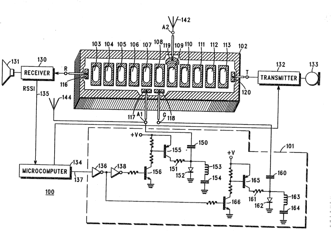
~, 10 Referring to Figure 1, there is illustrated a duplex
radio transceiver 100 including two antennas 142 and 144
!j, coupled to a single-block filter 102 shown in perspective
and embodying the present invention for providing both
antenna duplexing and antenna-switched diversity. Duplex
radio transceiver 100 also includes receiver 130 coupled to .
speaker 131, transmitter 132 coupled to microphone 133,
diversity control circuitry 101 coupled to antenna 144, and
''t microcomputer 134 coupled to receiver 130, transmitter
132 and diversity control circuitry 101 for controliing the
operation thereof. Blocks 130, 131, 132, 133 and 134 of -
transceiver 100 may be componen~s of any commercially
available duplex radio transceiver. In the preferred -~
embodiment, transceiver 110 is the transceiver shown and
described in Motorola instruction manuai number
68P81070E40, entitled "DYNATAC Cellular Mobile
Telephone," published by and available from Motorola C ~ E -
Parts, 1313 East Algonquin Road, Schaumburg, Illinois
60196.
According to the present invention, single-block
filter 102 is coupled to antennas 142 and 144 for providing ~ -
both antenna duplexing and antenna-switched diversity.
Antenna 142 is coupled by filter 102 to transmitter 132,
and antellnas 142 and 144 are switchably coupled by filter
102 to receiver 130 by diversity control circuitry 101 in ;
~J
~, ~
2~2a7~8 :
/ - 4 - CE00142R ~ ~ -
'~!''` response to diversity control signal 137. Microcomputer
134 is coupled to receiver 130 ~or monitoring the received
si~nal strength indication (RSSI~ signal 135. Wh~n the
RSSI signal 135 drops in lav~l indicating that the signal
5 being received on one of the antennas 142 or 144 has
~, become degraded due to fading or other interference,
'3`, microcomputer 134 chang~s the binary state o~ diversity
~i control si~nal 137 for switching receiver 130 to the other
one o~ antennas 142 or 144.
.. 10 Diversity control circuitry 101 includes pin diodes
152 and 162 which are switched in response to di~ersity
control signal 137 for switching receiv&r 130 between
antennas 142 and 144. When antenna 144 is selected, pin
, diode 152 is switched off and pin diode 162 is switched on
to couple pad 118 of filter 102 to RF signal ground.
Atternatively, when antenna 142 is selected, pin diode 162 ~ P~
is switched off and pin diode 152 is switched on to couple
i~ pad 117 of filter 102 to RF signal ground. Pin diodes 15
and 162 are switched on and off in response to the binary
state of diversity control si~nal 137.
When diversity control signal 137 has a binary one
state, the output of inverter 136 has a binary zero state
(low voltage) and the output of inverter 138 has a binary
,,t~ one state (high voltage). The binary one state of the output
of inverter 138 turns on transistor 156. When transistor -
156 is on (conducting current), transistor 155 is turned on - -~
and applies a bias curren~ to pin diode 152 via resistor
151. Pin diode 152 is switched on (low impedance state)
by this bias current and couples pad 117 and antenna t44 ~ `~
via capacitor 150 to RF signal ground. Pad 117 is
j preferably coupled by a coaxial cable or alternatively a
transmission line to capacitor 150 and antenna 144. It is
also preferable that capacitor 150 and pin dioda 152 be
located as çlose to the end A1 o~ such coaxial cable as -;
3 : ~
i~
.~
,~
i.~ ` . : .
.,,,~ . .
.
::
2 ~ 2 ~ ~ ~ 8 : :
- 5 - CE001421'~
, ~
practical. At the same time, the binary zero state of the
`. output of inverter 136 turns off transistors 166 and 165,
keeping pin diode 162 off ~high impedance state). Inductor
163 and capacitor 164 are coupled in parallel with pin
diode 162 for resonating out parasitics due to pin diode i-~
162 to achieve better open and short circuit conditions.
Conversely, when diversity control signal 137 has a
~5 binary zero state, the output of inverter 136 has a binary ~ -
-~ one state (high voltage~ and the output of invortar 138 has
.~ 10 a binary zero state (low voltage). The binary one state of
ths output of inverter 136 turns on transistor 166. When
transistor 166 is on (conducting current), transistor 165 is
, turned on and applies a bias current to pin diode 162 via ;. `
'! resistor 161. Pin diode 162 is switched on (low impedance
~, 15 state) by this bias current and couples pad 118 via
-I capacitor 160 to RF signal ground. Pad 118 is preferably
coupled by a coaxial cable or alternatively a transmission -
line to capacitor 160. It is also preferable that capacitor
160 and pin diode 162 be located as close to the end G of ~.
such coaxial cable as practical. At the same time, the
binary zero state of the output of inverter 13B turns off
;~ transistors 156 and 155, keeping pin diode 152 off (high
impedance state). Inductor 153 and capacitor 154 are
~, coupled in parallel with pin diode 152 for resonating out
parasitics due to pin diode 152 to achieve better open and -~
short oircuit conditions. ~ -
Filter 102 in Figure 1 is a dielectric block filter
preferably comprised of a high-dielectric low-loss
ceramic. Filter 102 may also be partially enclosed in a
housing, such as housing 280 shown in Figure 2, which
housing may be attached by soldering or other means ~ ~ `
producing a modular filter component. Filter 102 includes ;-
transmission line resonators formed by elongated holes
103-113 extending from the top surface to the bottom
, ,
.,
.
2~2~7~8
- 6 - CE00142R
`~ surface thereof. Holes 103-113 have a substantially
rectangular cross section with rounded corners and parallel
elon~ated sides. The boffom and sides of filter 102 and
;~ internal sur~aces of holes 103-113 are covered with
. 5 conductive material over substantially their entire
surfaces. The top surface of filter 102 is covered by a
strip of conductive material near the periphery thereof
which substantially surrounds holas 103-113. Also
-~ disposed on the top surface are pads for each hole 103-
113, pad 120 coupled by a coaxial cable ( at end T) to
,i transmitter 132, pad 116 coupied by a coaxial cable ~ at
l end R) to receiver 130, pad 119 coupled by a coaxial cable (
~, at end A2) to antenna 142, pad 117 coupled by a coaxial
cable ( at end A1) to antenna 144 and capacitor 150, and
pad 118 coupled by a coaxial cable ( at end G) to capacitor
160. The pads for each hole 103-113 and pads 116-120 are
likewise comprised of conductive material covering the top -
surface of filter 102. The pads for holes 103-113 may
;i~ have varying shapes for capacitively intercoupling with one --
another and coupling to the surrounding conductive
material at the sides o~ filter 102. Each of the holQs 103-
113 functions essentially as a foreshortened transmission
line resonator. In the preferred embodiment, the
conductive material covering the surfaces of filter 102 is
plated thereon.
When pad 117 is coupled to RF si~nal ground and pad
~`~ 118 is not grounded, filter 102 functions as a duplexer
coupling receiver 130 and transmitter 132 to antenna 142.
Conversely, when pad 118 is coupled to RF signal ground,
receiver 130 is coupled via pad 117 to antenna 144,
grounded pad 118 isolates receiver from antenna 142, and
,'3 transmitter 132 is coupled to antenna 142. The amount of
isolation provided by grounding pad 118 can be varied by
increasing or decreasing the capacitive coupling between
,,~
~,
..
.,~j .
~, .. ~ . ~ . .. . .
";. ~:,
~ 2~2~7~
.
- 7 - CE00142R -
~,-.
pad 118 and the pad for hole 108, by decreasing or ~ -
ij increasing, respectively, the gap between pad 118 and the
pad for hol~ 108, by varying the size of the opposing edges
of pads 108 and 118, or by any other suitable means. The ;
amount of couplin~ provided by pad 117 can likewise be
-~ varied with respoct to ~he pad for hole 107. In other
embodiments, pad 118 may be directly ccnnected to hole
108 or may be a portion of the pad for hole lG8.
3 Referring next to Figuro 4, there is illustrated a flow m
chart of the process usad by the microcomputer 134 in
Figure 1 for selecting between the antennas 142 and 144.
Entering at START block 402, the process proceeds to block
404, where the guard time flag is checked. If ~he guard
time flag has a binary one state, YES branch is taken to
block 408. At block 408, a check is made to determine if ; ~;
the four millisecond timar (4 MS) has timed out. If not, NO
branch is taken to RETURN block 420 ~o return to other
J tasks. If the four mitlisecond timer (4 MS) has tirned out, ~;
YES branch is taken from block 408 to block 409 where the
guard time flag is reset to a binary zero state. Thereafter, ~ -
program control proceeds to block 410 as described
hereinbelow.
Returning to block 404, if the guard time flag has a
binary zero state, NO branch is taken to block 406, where a
check is made to determine if the ten millisecond timer ~
(10 MS) has timed out. If not, NO branch is taken to RETURN - - ~ ~;
block 420 to return to other tasks. If the 10 MS timer has
timed out, YES branch is taken from block 406 to block 410 -~
where an RSSI sample is taken. Block 410 is also reached
from blocks 408 and 409 after the 4 MS timer has timad - -~ -
out. Microcomputer 134 includes an analog-to-digital ;~
converter for taking a di~itized sample of the RSSI signal
135. Next~ at block 412, a check is made to determine if
~ ~.
2~2~7~8 - -
- 8 - CE00142R
the RSSI sample is 6 dB less than ~he average RSSI. The
~` average RSSI is a running averago taken by microcomputor
134 over the last fifty RSSI samples. If the RSSI sample is
;'i not 6 dB less than the average RSSI, NO branch is taken
5 from block 412 to block 414 wh~re the average RSSI is
updated using the current RSSI sample, andl the 10 MS timer
is restarted for another ten millisacond time interval.
Thereafter, program contrel returns to other tasks at
,t RETURN block 420.
Returning to block 412, if the RSSI sample is 6 dB
less than the average RSSI, YES branch is taken to block
i' 416 where the binary state of the diversity control signal
137 is changed to switch between antennas 142 and 144. ~ -
Next, at block 418 the guard time flag is set to a binary one
15 statc, and the 4 MS timer is restarted for a four
millisecond time interval. The guard time flag is set in
order to sample the RSSI signal 135 four milliseconds
- after switching between antennas 142 and 144. As a --~
result, RSSI signal 135 will be sampled again after four -
20 milliseconds rather than ten milliseconds. The sampling ~ n~
interval is reduced in order to be sure that the antenna 142 ~ -
or 144 being switched to is rec~iving an adequate RF
signal. If both antennas 142 and 144 are receiving poor RF
signals, receiver 130 will be switched from one antenna to
25 the other every four milliseconds. Thereafter, program
control returns tc other tasks at RETURN block 420.
Referring to Figure 2, there is illustrated another
filter 202 embodying the present invention. Instead of ~-
usin~ pads for coupling signals theretoi filter 202 includes
3û coupling electrodes 216, 217, 218, 219, and 220, which
`~ extend at least partially into corresponding holes 203, 207,
208, 209, and 213, respectively. Electrodes 216-220 are
positioned and retained in holes 203, 207, 208, 209, and
213 by means of dielectric plugs 226-230, respectively.
~,
., .
- :
.
:
. .
2~2~7~
- 9 - CE00142R ~ ~
, . -.
Plugs 226-230 may be comprised of any suitable - :.
. dielectric, such as, for ~xample, ceramic or plastic. Plugs
226-230 may be retain~d in holes 203, 207, 208, 209, and ~
~' 213 by means of a press fit, glue, or other suitable means. ;~.-
,~ 5 Plugs 226-230 may also be loosely fitted in holes 203,
207, 208, 209, and 213 and retained thereirl by a housing
280 which extends over plugs 226-230 and has holes ..
therein allowing electrodes 216-220 to protrude
therefrom. Once housing 2~0 is attached by soldering or ~ - .
other suitable means, filter 202 may be mounted on a ~ ~-
printed circuit board (not shown3 as a modular filter
component. . -
P~eferring to Figure 3, there is illustrated a unique
coupling el~ctrode 216 having a flat portion 316, 317
extending at least partially into a corresponding hole 203
of filter 202 for coupling signals thereto. Electrode 216 -
inserts into plug 326, which includes a top portion 226 and ~ r ~-
a rectangular shaped hold 318 for accepting flat portion
316, 317 of electrode 2t6. Electrode 216 may have a shape
2û and size that varies for varying the amount of coupling to ~ -~
the resonator provided by hole 203. For example, eleotrode
216 may have a rectangular shape 317 or triangular shape
316. In other embodiments, electrode 216 may simply be a
pin. Coupling slectrodes 217, 218, 219, and 220 and -:
2~ correspondin~ plugs 227, 228, 229 and 230 may also be
implemented as shown in Figure 3.
Referring to Figure 5, there is illus~rated a top view
of yet another single-block filter 500 embodyin~ the `~
present invention, which has two antenna pads 524 and
526. The embodiment in Figure 5 makes better use of the
isolation characteristics of filter 500. Pad 524 is a strip
; of conductive material located between holes 508 and 509, ~ ~
and pad 526 is also a strip of conductive material located ~ ~ -
between holas 509 and 510. Pad 524 extends from the -
;l ::-
, ~.:. .
'~3 ~ :.
~j " "
'.:.:.: ' ' : :
2Q2~7~8
.. ~ .
~ - 10 ~ CE001 42R
, . opposite side of filter 500 as does pad 526. The width,
length and positioning of pads 524 and 526 may be varied
to vary the coupling to corresponding holes 508, 509 and
509, 510, respectiv~ly. Pad 526 couples antenna terminal
.` 5 A2 to resonators 509 and 510. Switch 522 is responsive to -~
diversity control signal 137 for switching pad 524 to
either antanna terminal A1 or antenna terrninal A2. Switch
522 may be implemented with one or more conventional
reed relays or with pin diodes and transmission line
circuitry. The pads for holes 503-513 of filter 500 have ;~
.~ varylng shapes for capacitively intercoupling with one
another and coupling to the sùrrounding conductive
material at the sides of the block.
Referring to Figure 6, there is illustrated a top view
of yet a further singla-block filter 600 embodying the
present invention, which has two antenna pads 624 and
626. The embodiment in Figure 6 makes better use of tha
isolation characteristics of filter 600. Pad 624 is a strip ~ ~ `
;~ of conductive material located between holes 608 and 609,
: `,1
and pad 626 is also a strip of conductive material located
between holes 609 and 610. Pad 624 extends from the
same side of filter 600 as does pad 626. The width, length
and positioning of pads 624 and 626 may be varied to vary
the coupling to corresponding holes 608, 609 and 609, 610,
respectively. Pad 626 couples antenna terminal A2 to
resonators 609 and 610. Switch 622 is responsive to
~j diversity control signal 137 for switching pad 624 to
either antenna terminal A1 or antenna terminal A2. Switch
622 may be implemented with one or more conventional
~', 30 reed relays or with pin diodes and transmission line
circuitry. The pads for holes 603-613 of filter 600 have
varying shapes for capacitively intercoupling with one
another and coupling to the surrounding conductive
.' material at the sides of the block.
'!! ; `:-
!' ' ` .
:~:
., ~,
.~.; ' .
~ 20~7~8
: ; .',
- 11 - CEOû142R
!~ In summary, a unique single-block fi!ter has been
~`~i` described which is capable of providing both antenna
duplexing and antenna-switched diversity in a duplex radio - .
transceiver. The unique single-block filter rnay include
coupling electrodes and a housing for providing a modular ;~
filtsr component. Moreover, the single-block filter may --
include unique coupling electrodes having a flat portion
~, extending at least partially into corresponding resonators
thereof for coupling signals there~o. The unique single-
block filter and unique coupling electrodes of the present
s. invention may be advantageously utilized in applications ~ -
where RF filtering, antenna duplexing and/or antenna
diversity is desired. ;
.!:1 '
`';~ : ~
`I ' '`,.,:
.. . .
,j~ . .
'l . -
,,, ; "
,. . .
,.
,,.. ,.,~ ~., .~ . . - - . .. - .. . -.