Note: Descriptions are shown in the official language in which they were submitted.
AC ~O DC TO AC POWER CONVERSION
APPARATUS WIT~ FEW ACTIVE SWITCRES
AND INPUT AND OUTPUT CONTROL
FIELD OF THE INVENTION
Ihis invention pertain~ generally to the field of
electrical power conversion systems and particularly to
power converters utili~ed in uninterruptable power supply
systems and single to three phase converters.
~ACKGROVND OF THE INVENTION
Uninterruptable power supplies (UPS) are widely
applied for a variety of critical loads, including
computers, financial tran~action handlers and life Rupport
equipment. A proliferation of power electronic load~ on
the utility grid has caused a significant increase in
harmonic levels on the AC lines. Further, the use of
computers on a very large scale has made the issue of the
cleaness of the power available on the power system more
critical. Although UPS ~ystems have been used in the paqt
for large computer installations, the increased dependency
of business and industry on computers has seen a
tremendous increase in the use of UPS systems even for
2~25~
-- 2 --
small computers operating off single phase ~upply lines.
Given the decreasing cost of computing capability,
single phase UPS systems are extremely sensitive to cost.
Con~equently, few UPS manufacturers can afford the luxury
of offering improved power factor interface to the
utility. However, the possibility of harmonic standards
being enforced is very real, and more importantly, the
restriction of RMS current supplying capability for
commercial or domestic line frequently limits tlle rating
of the ]argest unit that can be fed from the available
supply. Consequently, units with a poor power factor will
be able to draw less power from the supply mains than a
comparable unit with sinusoidal input line currents. A
third harmonic overload in neutral conductors is another
result of AC line current harmonic~, and are often
encountered in the use of typical UPS systems and switched
mode power supplies.
Two approaches have primarily been utilized for
commercial UPS systems. One approach uses a
ferro-resonant transformer as a voltage regulator. Line
conditioning i6 completely passive and the technique is
very robust, giving good immunity against disturbances.
Under normal operation therefore, power flow does not
occur through the transfer devices. On identifying
failure of the AC line,`the inverter is brought on line,
the connection to line power is cut off, and the inverter
continues supplying the load. During normal operation,
the inverter can also be used to recharge the battery.
This technique has high efficiency and reliability as well
aQ moderate cost. However, the ferro-resonant transformer
tends to be fairly heavy, and transitions from AC line to
inverter operation can encounter problems under certain
low or high line conditions. The quality of the output
waveform under non-linear loads can also be very poor.
The other common approach is the so-called on-line UPS
system in which a separate AC to DC converter i~ used to
2 ~ 4 7
-- 3 --
provide battery charging and regul~tion function. The DC
bus is supported by the battery and feeds a DC to AC
inverter with appropriate filtering. Static by-pa~s
switches are used to revert the output power to the AC
line in the event of failure of the inverter. Such a
scheme provides power from the main power lines under
normal operation, but only after two stages of power
processing. Consequently, although the system has good
performance, it is more expensive and less efficient.
Another approach reported recently may be referred to
as a stand-by utility interactive UPS system. See, T.
Kawabata, et al., "Chargerless UPS Using Multi-Functional
Mi-MOS Inverter," IEEE-IAS Conf. Rec., 1986, pp. 513-520.
Using such a technique, the need for two power conversion
stages is eliminated, and the inverter charges a high
voltage DC battery while the system is in the stand-by
mode. This approach, however, allows no line conditioning
in terms of voltage correction, disturbance rejection, or
reactive/harmonic compensation. The approach can be
varied so that the inverter is used to simultaneously
function as an active filter to improve the line current
waveform, as well as to maintain the state of the charge
on the battery. This approach requires higher inverter
ratings and bulky series filter components.
High fre~uency link ~ystems which would result in
substantial reductions in transformer si~e and cost have
been proposed. See, e.g., S. Manias, et al., "Bilateral
DC to AC Converter Employing a Hish Frequency Link," IEEE-
IAS Conf. Rec., 1985, pp. ; I. Yamato, et al., "New
Conversion System For UPS Using High Frequency Link,"
IEEE-PESC Conf. Rec., 1988, pp. 658-663. While the
concept of high frequency links is very sound, its
usefulness in UPS applications may be questionable. Upon
inverter failure, the bypaæs arrangement now has to he
accomplished without isolation. If the system is to
operate under those conditions for any length of time, it
202~8~7
- 4 -
may not be acceptable. Further, the presence of a static
bypass arrangement already involves non-iso1ated contact
between the supply and load sides, completely obviating
the function of the high frequency transformer. However,
the objectives of UPS availability can al80 be provided
for by multiple units operating in parallel.
None of the approaches aiscussed above simultaneously
satisfy the requirements of load regulation with nonlinear
loads, single stage power conversion, small filter
components, and sinusoidal AC line currents with unity
power factor.
SUMMARY OF THE INVENTION
m e present invention provides a power conversion
apparatus having a minimum number of active switches and
is especially adapted to single phase UPS systems. It
takes advantage of the fact that power flow in most UPS
applications is completely unidirectional, that is, from
AC line to load. The conversion apparatus requires the
utilization of only four active switches to realize its
objectives. These include independent control of the
input and output currents, a common neutral connection,
line conditioning, sinusoidal input currents independent
of load currents, a~ well as battery charge and discharge
regulation. Five switches may be utilized if a low
voltage battery and resonant link operation is desired.
The power conversion apparatus of the invention allows
full control of the currents on the load and AC lines
sides, even when the input and output are completely
asynchronous. The apparatus can operate with unity input
power factor and deliver a high quality waveform to the
load.
~ -e conversion apparatus of the invention includes a
full bridge of active switching devices connected across
DC bus lines to which the battery is also connected. The
2 iO ~
single phase input line supplies rectified power to the DC
bus through a rectifier bridge. The load and the AC
supply line share a common neutral line. The switching of
the switching devices in the bridge is controlled to
provide AC output power to the loa~ through a
transforDer. ~tatic switches can be connected in the line
from the bridge inverter to the transformer, and another
static switch can be provided in a line directly from the
supply line to the transformer, to allow the inverter to
be switched out and thereby operate the load directly from
the AC supply lines until a line failure is detected. The
inverter can also be operated to provide line conditioning
and distrubance rejection while power i8 being supplied
from the main AC power lines, and allows the backup
battery to be charged during stand-by operation.
The apparatus of the invention can also be implemented
utilizing a resonant DC link and a fifth active switch can
be employed to convert the circuit to a soft-switching
resonant D~ link converter, allowing the u6e of a lower
voltage battery. This permits switching frequencies whic~
are an order of magnitude higher than in conventional hard
switching inverters.
Further objects, features, and aavantages of the
invention will be apparent from the following detailed
description when taken in conjunction with the
accompanying drawings.
BRIEF DESCRIPTION OF THE DRAWING
In the drawings:
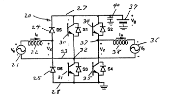
Fig. 1 is a schematic circuit diagram of a power
conversion apparatus in accordance with the invention with
input and output control.
Fig. 2 are illustrative voltage waveforms for DC
modulation of the conversion appparatus of Fig. 1.
Fig. 3 is a plot showing the locus of possible values
of the battery voltage for the conversion apparatus of
Fig. 1.
'~ 7
- 6 -
Fig. 4 is a sehematic circuit diagram for a UPS syste~
utilizing the present invention.
Fig. 5 is a schematic circuit diagram of a single
phase to three phase converter incorporating the
conversion apparatus of the present invention.
Fig. 6 iB a schematic circuit diagram of a UPS power
conversion apparatus utilizin~ a resonant DC link
connected to the battery.
Fig. 7 is a block diagram of a load side controller
for a USP ~ystem in accordance with the invention.
Fig. 8 is a block diagram of the synthesis of the
input AC line reference I~.
Fig. 9 is a block diagram of a controller for the UPS
system of Fig. 4 which accomplishes simultaneous control
of the input and the output.
Fig. 10 are waveforms for the resonant DC link
inversion apparatus of Fig. 6 including output voltage,
inductor current, inverter line to line voltage, and
inductor current, supply voltage, and supply current.
DETAILED DESCRIPTION OF THE INVENTION
A schematic circuit diagram of the basic power
conversion apparatus of the invention is shown generally
at 20 in Fig. 1. The apparatus receives AC power from a
single phase source 21, which may be AC power mains,
through an input inductor 22, which may represent an input
tran~former inductance. The influctor 22 is connected to a
node 23 between a pair of diodes 24 and 25 to rectify the
input AC current passed through the inductor 22 to a DC
current and a DC voltage between DC bus lines 27 and 28.
Also connected across the DC bus lines 27 and 28 is a
inverter bridge formed of gate controlled active switching
devices 30, 31, 34 and 35. Each of these switches, which
may be bipolar junction transistors, typically would
include antiparallel diodes as shown in Fig. 1. The
-- 7 --
electrical connection between the switches 30 and 31 i8
joined at a node 32 to a common neutral line 33 which
extends from the input power source to the output load 36,
represented a~ a voltage source in Fig. 1. The output of
the bridge composed of the switches 30, 31, 34 and 35 is
supplied from a connection at a node 37 to an output
inductor 38 (which may repre~ent an output transformer
inductance) which delivers the current passed through it
to the load 36. The backup ~torage battery 39, or output
filter if required, is connected to the DC bus line 27, as
is a smoothing capacitor 40.
The inverter bridge operates under a pulse width
modulation strategy which chooses one of three switching
states (+1, 0 and -1). The choice of the zero state can
be fullfilled by turning on switches 30 and 34 (zero
positive, 0+) or 31 and 35 (zero negative, 0-)
simultaneously, with no discernible difference from the
point of view of the load. This fact represents an
additional degree of freedom which can be exploited to
control the AC line side current.
For example, if the current I8 flowing through the
inductor 22 is positive as shown in Fig. 1, the diode 24
is seen to be conducting. By selecting the switches 30
and 34 to realize the zero state (01), zero volts is
impressed across the input lines (the voltage Vx), while
selecting the switches 31 and 35 (0-) results in the DC
bus voltage VB (the voltage of the battery) as the
voltage Vx between the node 23 and the common line 33.
For positive voltage from the voltage source, Vs, this
results in the current I8 increasing or decreasing,
rèspectively. Simil~rly, for negative values of V8 and
Is~ the diode 25 conducts and selecting the 0+ state
gives Vx = ~Vv while the 0- states gives Vx =
The diodes 24 and 25 constrain power flow to be
unidirectional from the AC lines to the DC bus capacitor
40. Thus, the circuit functions in the manner of a
semi-controlled converter with active switches.
~2~7
-- 8 --
The degree of control available on the input side
depends strongly on the number of times the inverter is
allowed to choose the zero state. This 1mplies that a
higher ratio of VB to VO is required to obtain good
control on both sides. On the other hand, every selection
of a non-zero state reduces the amount of control
available for the input sides. Consequently, full control
on both the input and output sides is only available over
a restricted range of input and output voltages.
This relationship can be examined by considering DC
input voltages assuming pulse width modulation control3.
If such DC input voltages are provided (rather than the
normal AC from the power mains), the resulting waveforms
for the voltages V and V are shown in Fig. 2. The
inverter operates between the state 1 (switches 30 and 31
conducting) and state zero with a duty cycle Di to give
a positive output voltage VO. For positive values of
V8 and I8, the diode 24 conducts all the time. As the
switches 31 and 34 conduct for Di, the voltage Vx is
contrained to be at the DC bus level VB at least for
that period of time. During the time that the inverter is
in the zero state, the O~ or O- state can be chosen to
acheive the desired control. For DC input voltages this
gives the following relationships.
Vo = Di VB
V8 ~ Di VB VO
Consequently, if full control on input and output are to
be`obtained, V8 must be greater than VO. Similarly
for negative values of VO and for positive values of
V8, the relationships are seen to be:
VO - -~l-Di) VB
V8 Di VB = 1 + Vo/VB
`:~
`.
~02~7
g
For negative values of Vg, a similar set of equations
can be determined. These contraint equations are
illu~trated in the graph of Flg. 3 and show that, ln the
steady ~tate, if both V9 and VO have the same
polarity, then the converter works as a buck converter and
has a limitation on the maximum poqsible output voltage
that can be realized. Where VO and V8 have opposite
polarity, any ratio of VO to V8 can be obtained.
However, there is a maximum ~imultaneous voltage
limitation on VO and Vs of 1/2 the DC bus voltage.
These limitations are important if input and output
control are to be fully maintained under DC conaitions.
Under AC operations, the energy storage in the DC link can
substantially alter the behavior of the converter.
The foregoing AC to DC to AC conversion apparatus can
be adapted for UPS operation as shown in Fig. 4. The
i~portant requirements now include maintaining charge and
discharge of the storage battery on the lin~, in addition
to regulation of the input and output currents. The load
side output may be controllea using a current regulator,
in accordance with output voltage regulation and
distortion requirements. The input side may also be
current regulated, and the reference command is calculated
based on battery charge and discharge needs as well as
load demands.
The UPS system in accordance with the present
invention is shown generally at 50 in Fig. 4 and receives
AC line power on AC terminals 51 and 52 from the power
mains. One of the terminals 52 is connected to the common
or neutral line 53 of the apparatus, w~ile the other
terminal Sl is connected to an input inductor 54 which
supplies current to a node 55. The node 55 is connected
between a pair of diodes 56 and 57 which are connected
across the DC bus line 58 and ground. A bridge inverter
formed of four active switching device~ 59-62 is also
connected across the DC bus 58 and ground in a manner
20~8~7
-- 10 --
similar to that described above with respect to the~
circuit of Fig. 1. The node 63 between the switching
devices 59 and 60 is connected to the common line 53 and
the node 64 between the switching devices 61 and 62 is the
output voltage connection from the bridge. Also connected
to the DC bus are a smoothing filter capacitor 65 to
ground and a battery 66 through a filtering inductor 67.
The output voltage from the brid~e at the node 64 is
supplied through an output inductor 70, a controllable
static switch 71 and a line 72 to a tap in the primary of
a transformer 74. The secondary of the transformer 74 is
connected to an output line 75 leading to the load, with
the capacitor 76 connected across the line 75 to filter
output transients. To complete the circuit, a
controllable static switch 78 is connected in a line from
one of the AC input terminals 51 to the primary of the
transformer 74. Thus, when the static switch 78 is
closed, the voltage acro~s the AC input lines 51 and 52
will be provided acro~s the primary of the transformer 74.
The system of Fig. 4 can operate as an on-line UPS and
provide line conditioning and distubance rejection. The
transformer tap is selected such that under low-line
conditions the converter bridge formed of the devices
59-62 can adequately supply the load. During the bypass
mode, the static switches 70 and 78 are activated to
directly connect the load to the primary of the
transformer. A particularly desirable feature of this
circuit i~ the use of a common neutral connection between
the input line at the terminal 52 and the output at the
primary of the transformer 74.
The AC to DC to AC conversion apparatus of the
invention can also be adapted to be utilized as a single
phase to three phase converter, as illustrated generally
at 80 in Fig. 5. The system 80 receives single phase AC
power at input terminals 81 and 82 but has a third
202~7
-- 11 --
terminal 83 on which is generated a voltage which
effectively causes the power across the three terminals
81, 82 and 83 to be a three phase voltage which may be
applied to a three phase load, such as the motor 8~
illustrated in Fig. 5. The input voltage on one of the
terminals 81 i8 provided through an input inductor 86 to a
node 88 at which rectifying diodes 89 and ~0 are joined.
The output of the diodes 89 and 90 is provided to DC bu~
lines 91 and 92 across which is connected a bridge
inverter composed of active switching devices 93-96. At a
node 98 a connection is made between the switching devices
93 and 94 and the second AC input terminal 82. The output
of the inverter at a node 99 connected between the
switching devices 95 and 96 is connected to the third
terminal 83. A capacitor 100 is connected across the DC
bus to smooth out the voltage on the bus and provide a
stored DC voltage across the bus lines.
Because the output inverter composed of the switching
elements 93-96 can supply voltage and current having an
arbitrary phase/frequency relationship with the input, and
because the neutral connection at which the input terminal
82 i B connected to the node 98 is common, the inverter can
be made to synthesize a waveform with the same voltage as
the input, but phase shifted so as to generate a balancea,
three phase voltage. This inverter can then be used to
drive a three phase load indicated by the motor 84, for
example, a constant speed induction machine.
The use of high voltage batteries in UPS systems often
creates reliability and C08t issues. To use a lower
voltage battery nor~ally requires extra devices to perform
the bi-directional chopper interfaces between the battery
and the DC link. ~owever, the conversion apparatus of the
present invention can be readily adapted to be utilized as
a soft switching resonant DC link inverter with
frequencies which are an order of magnitude higher than
conventional hard switching inverters. This resonant link
~2~
- 12 -
circuit is illustrated generally at 110 in Fig. 6.
Operation with bipolar junction transistors (BJT)
darlingtons at 30 kHz for 15 kVA inverters is easily
feasible. With IGBTs and new devices such as the MCT,
1ink frequencies up to 60 kHz are pos 8 ible. The circuit
is easily realized at the multi-kilowatt power levels of
interest. The u~e of a ~oft switching circuit achieves
substantial benefits in terms of the size of filter
components, acoustic noise, electromagnetic interference,
and system efficiency.
The high frequency DC link conversion apparatus 110 of
Fig. 6 receives single phase power at input terminals 111
and 112, with one of the terminals connected to an input
inductor 114 and the other connected to a common output
line 115. The inductor 114 i8 connected to a node 116
that joins two diodes 118 and 119. The diodes 118 and 119
are connected between DC bus lines 120 and 121, as is an
inverter composed of gate controlled active switching
devices 123-126 connected in a bridge configuration. The
junction between the switching devices 123 and 124 at a
node 127 is connected to the common line llS, and the
junction between the switching devices 125 and 126 at a
node 128 is connected to an output line 129 leading to an
output inductor 130 which extend to one of the output
terminals 131, to which the UPS load may be connected.
The other output terminal 132 is connected to the common
line 115, and an output filtering capacitor 133 is
connected between the terminalY 131 and 132.
A capacitor 135 i~ connected between the DC bus line
120 and 121 and charges to provide a DC voltage across
these lines. The battery 137 is connected to the DC bus
line 120 by a resonant link circuit composed of a series
inductor 138 and an active switching device 140. A
capacitor 141 and inductor 142 are also connected to the
DC bus line 120 and are joined at a node 145 to which the
battery is also connected. A capacitor 144 extends from
2 ~
- 13 -
the node 145 to connection to the other DC bus line 121.
The switching oP the device 140 can be controlled to
provide a resonant DC link voltage on the DC bus 120 in a
conventional manner. See, for example, D. M. Divan, et
al., "Zero Voltage Switching Inverters for High Power
Applications," IEEE-IAS Conf. Rec. 1987, pp. 625-639, and
. Venkataramanan, et al.,"Discrete Pulse Modulation
Stategies for High Frequency Inverter Systems," IEEE-PESC
Conf. ~ec., 1989, which are incorporated herein by
reference.
~ variety of control options are available for
providing simultaneous regulation of input and output
currents as well as battery charging functions. For
example, a block echematic of a controller required for
synthesizing to two reference currents I and Io
is shown in Fig. 7 and 8. See, also, the article by
Venkataramanan, et al., supra. To obtain good output
regulation, especially in the presence of non-linear
loads, a current regulator with reference and load
feedforward is used. The reference output voltage V
is applied to a block 150 in Fig. 7 corresponding to the
filter capacitor. This represents the fundamental
component Ic that must flow in the capacitor if the
desired output voltage i~ to be obtained. The current
Ic is added at a junction 151 to the fundamental load
current from Il a line 152 to generate a current
reference Io for the converter section. The load
current is considered to be a disturbance to the syetem,
and is aleo compensated using feedforward on a line 154 to
a summing junction 155 which also receives the value of
Io through a current regulator 156. This approach gives
extremely good dynamic characteristics as well as voltage
regulation, even in the presence of substantial load
non-linearities. The output of the junction 155 is
integrated (156) to provide the output voltage V which
ie compared in a summing junction 160 with the reference
2~25~
- 14 -
V0 and the difference is passed through a
proportional-integral compensator 162, the output of which
is supplied to the summing ~unction 151.
The input current reference V is derived from
the dual requirements of DC bus regulation and battery
charge and discharge requirements. The battery voltage
VB is compared at a summing junction 170 with a
reference voltage Vbatt der~ e
reference battery current Ibatt and the differences
is provided to a proportional-integral controller 172, the
output of which is provided to a multiplying junction 174
which also receives the supply voltage V . The
proportional-integral controller is used to accomplish
power balance, taking into account the powerflow into the
battery. The output of the proportional-integral
regulator is multiplied with the input supply voltage Vs
to realize a template for the input current waveform
I .
For the hard switching pulse width modulated (PWM)
system of Fig. 4, a two output variation of the dead-beat
control proposed in K. P. Gokhale, et al., "Dead-Beat
Microprocessor Control of PWM Inverter for Sinusoidal
Output Waveform Synthesis," PESC 85 Conf. Rec., pp. 28-36,
is possible. However, the resonant DC link inverter of
Fig. 6 is capable of superior performance. Control using
discrete pulse modulation stategies, necessary in resonant
link systems, requires a different approach. In PWM
systems, the existence of a finite switching period
implies the concept of an average value over a cycle,
defined by the duty factor. In discrete pulse modulation,
where only the possible switching instants are know, there
is no equivalent period of repetition. Con~equently, open
loop systems are virtually impossible to implement, and a
closed loop regulator is required. This is not a drawback
in most implementations.
' ,~
"` 202~
- 15 -
The discrete pulse modulated current regulator can be
implemented in various ways. Most appealing ~ppears to be
an optimal co~t function regulator. See the article by
Vekatarmanan, et al., supra. Discrete pulse modulators
(DMP) systems which allow the selection of optimal
inverter states to ful$ill defined cost functions are
relatively easy to implement. A typical cost function
could be the following:
J = k~ Abs(I -I8) + Abs(Io-Io)
W~ere k i 8 a scaling factor which indicates the relative
importance of regulating Io or I8. The coæt function
J is calculated for all the four states ~l,0+,0-,-l~, and
the state which realizes the lowest value is selected.
This approach has been implemented in the past, but is
fairly complex.
A simpler iDplementation which give~ very good
performance uses the output vo]tage information. When
ever V0 is ~ufficiently large, it can drive the output
inductor current Io with sufficient slope to allow
current control. Under these conditions, the inverter
output is switched between an active vector (i.e., ll) and
zero. This permits control of the input side current.
Whenever the voltage V0 is close to zero, the inverter
is swtiched from one active state to another to control
the inverter current, but with one resonant link cycle
spent on the zero state. This implementation requires
comparators checking on the instantaneous errors in the
load and line ~ide inductor currents and a signal
indicating the presence of adequate back EMF. A simple
state sequencer i8 then sufficient to generate the control
functions needed.
A block diagram of the controller implemented in
accordance with the foregoing proceaures i8 illustrated in
Fig. 9. The I reference i8 generated in the same
,,~
202~8~'~
- 16 -
manner as illustrated in Fig. 8, and yields a value
I9 which is compared with the measured current value
I6 in a differential amplifier 180, the output of which
i9 provided as an input to a logic circuit 181 which
provides the gating control output~ to the four active
switches in the inverter. Another input to the logic
circuit 181 is provided from a differential operatianal
amplifier 183 which receives at its two inputs the load
current Il and the signal obtained from the output of a
summing junction 184 which receives inputs from another
summing junction 185 and from a gain control circuit 186
whlch provides a constant, K, to the signal applied
therqto. m e inputs to the junction 185 are the output
current Io and the reference voltage V0 passed
through the capacitor 187. The input to the gain function
186 i~ provided from a summing ~unction 190 which compares
the reference voltage V0 with V0. V0 is also
applied through an absolute value function 191 to one of
the inputs of a differential amplifier 192 which recieves
at its other input a scaled source voltage kV . The
output of the amplifier 192 is also provided to the logic
circuit 181. The circuit 181 al80 receives a link
sychronization signal on a line 194 which provides timing
information to properly time the gating signals to the
gates of the active switching devices in the inverter
bridge.
As an example of the implementation of the invention,
a conversion apparatus utilizing the resonant DC link
converter of Fig. 6 was implemented using BJT darlington
transistor modules switched at a link frequency of
27 KHz. A controller as described above with respect to
Fig. 9 was utilized which incorporates feetforward
concepts as well as a discrete pulse modulation strategy.
me waveforms of Fig. 10 illustrate the proper regulation
of the input an~ output currents as well as control boost
operation from the AC line to the DC link. The graphs in
202~8~7
- 17 -
Fig. lO show filter output voltage (200), output inductor
current Io (201), inverter line to line voltage (202),
input inductor current (203), supply voltage (204), and
supply current ~205). The line to line inverter output
voltage waveform confirm~ the modu]ation strategy where
plus and minus 1 transmissions are only permitted under
low back EMF conditions, and even then only after a one
cycle wait at a zero ~tate. The resonant DC link
converter implementation also realizes the benefit of low
acoustic noise, low electromagnetic interference,
excellent harmonic performance and dynamic performance,
and high efficiency.
It is thus ~een that the conversion apparatus in
accordance with the present invention allows the
achievement of several advantageous features. These
include the requirement for only four switches, or five
with a low voltage battery and resonant link operation,
boost control from the AC line to the DC link, independent
control of both input and output sides, a common neutral
between the input and output, line conditioning in
addition to a UPS function, sinusoidal input AC line
currents irrespective of the load current, and the
accomplishment of battery charge and discharge control
with no additional devices.
It is understood that the invention is not restricted
to embodiments ~et forth herein as illustrative, but
embraces all ~uch forms thereof as come within the scope
of the following claims.