Note: Descriptions are shown in the official language in which they were submitted.
2~25950
A DUPLEX STRUCTURE SIGNAL TRANSFER POINT SYSTEM
FOR COMMON CHANNEL SIGNALLING SYSTEM NO.7
[BACKGROUND OF THE INVENTION]
The present invention pertains to a duplex structure signal
transfer point system for common channel signalling system No.7
suggested by CCITT (International Telegraph and Telephone
Consultative Committee).
Unit level 2, one of the units which accept protocol for
message transfer, is a board that runs protocol level 2 of the
message transfer part protocol. Unit level 3 is a board that runs
message handling protocol, which governs message routing in
protocol level 3 of the message transfer protocol. Network level
2-3 interconnects the units such as a unit level 3, a network unit
level 3-3, and many unit level 2's And a signal message processing
sub-module, comprising the unit level 3, the unit level 2, and the
network unit level 3-3, is constructed by interconnection of each
unit with the network unit 2-3.
In prior art signal transfer point system, a network level
2-3 with only one path is used for the interconnection between the
unit level 3 and the unit level 2's. Also, a network level 3-3
with one path is used for the interconnection between such
modules. In case a path is malfunctioning, many unit level 2's or
modules are disabled given that there's just one path in such a
system.
2025~55
[SUMMARY OF THE INVENTION]
It is an object to irnprove the reliability of the
system by replacement of the malfunctioning module following
appropriate procedures.
To achieve the above-rnentioned ob~ect, the present
invention provides a duplex structure signal transfer point
systern for common channel signalling system No. 7, comprislng
(1~ a duplex structure network level 3-3, ~2! a network unit
level 3-3 interconnected to the duplex structure network level
3-3, a unit level 2, and a unlt level 3, (3~ a signal message
processing module with duplex structure network level 2-3,
interconnecting the unit level 3, the unlt level 2, and the
network unit level 3-3, (4) a management module connected to
the duplex structure network level 3-3, and (5~ an ~ & M
(Operation and Maintenance) systern connected to the duplex
structure network level 3-3.
In accordance with the present lnventlon, there ls
provlded a duplex structure slgnal transfer polnt system for
cornmon channel signalling systern No. 7, comprising: duplexed
serial interconnection mean~; duplexed network interface means
connected to said duplexed serial interconnectlon means, for
performing an interconnection between a plurallty of slgnal
message processing submodules; duplexed parallel
lnterconnectlon means connec~ed to said dllplexed network
interface means, for performing a parallel duplexed
interconnection between a plurality of unlt level 2 performlng
means and a duplexed unit level 3 performing means; sald
duplexed unlt l~vél 3 performing means connected to said
.~ 2 74~92-1
202~95U
duplexed parallel interconnection means, for performing a
protocol level 3 of a message transfer protocol in the common
channel signalling system No. 7; and said plurality of unit
level 2 performing means connected to said duplexed parallel
interconnection l-neans, for performing a protocol level 2 of
the message transfer protocol ln the common channel signalling
systern No. 7.
[BRIEF DESCRIPTION OF THE DRAWINGS]
This invention will be readily understood from the
following more detailed description presented in coniunction
with the following drawings, in which:
Flg. 1 is a diagram showing a duplex structure
signal transfer point system of the present invention;
Fig. 2 ls a diagram showing duplex structure slgnal
message process module of the present invention;
Fig. 3 is a dlagram showing duplex structllre signal
message process sub-modules of the present invention;
' 2a 74Q92-1
202~9~0
Fig.4 is a diagram showing streams of input signal messages
applied to unit level 2 ;
Fig.5 is a diagram showing construction of unit level 3 ;
Fig.6 is a diagram showing construction of inter-connection
network unit level 3-3 ;
Fig.7 is a diagram showing construction of unit level 2 ;
Fig.8 is a diagram showing a common DPRAM (Dual Ported Random
Access Memory) ;
Fig.9 is a diagram showing detailed construction of other
embodiment of unit level 2 ;
Fig.10 is a diagram showing detailed construction of other
embodiment of unit level 2.
[DETAILED DESCRIPTION OF THE DRAWINGS]
With reference to the drawings, the present invention will be
described in detail.
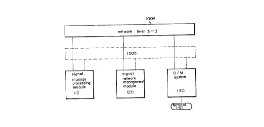
Fig.1 is showing a signal transfer point system with duplex
structure network level 3-3, comprising (1) network level 3-3's
100a and 100b, (2) a signal message processing module 110, (3)
a signal network management module 120, (4) an O & M (Operation &
Maintenance) system 130, and (5) a terminal 140.
Fig.2 is showing a duplex structure signal message processing
module of the present invention, comprising (1) network level
3-3's 200a and 200b, (2) a signal message processing sub-modules
220a through 220n.
Fig.3 is showing a duplex structure signal message processing
2025950
sub-module, comprising (1) network level 3-3's 300a and 300b, (2)
unit level 3's 310a and 310b, (3) network unit level 3-3 320a and
320b, (4) parallel buses or network level 2-3's 330a and 330b,
(5) unit level 2's 340a through 340n, (6) distributive memories
350a and 350b in the unit level 3, (7) distributive memories 360a
and 360b in the network unit level 3-3, and (8) distributive
memories 370a through 370n in the unit level 2.
In the present invention, the signal message processing sub-
module consists of two separate boards, the network unit level
3-3's 320a and 320b, for the interconnection between the duplex
structure network level 3-3's 300a and 300b. In this way, the
reliability of the system is improved given that the disable state
of a signal message processing sub-module is prevented by the
utilization of the network unit level 3-3's and the parallel buses
with no error, instead of the network unit level 3-3 and the
parallel buses with error. Especially, the unit level 3's 31Oa
and 310b are interconnected to numerous unit level 2's, 340a
through 340n, by two parallel buses, 330a and 330b. In case an
error occurs in a parallel bus of such a system, the disable
states of numerous unit level 2's, caused by the error on the
parallel bus, are prevented by the interconnection between the
unit level 2 and the unit level 3 through the parallel bus with
no error. As a result, the reliability of the system is improved,
and the system normally operates during maintenance. Two boards
of the unit level 3 can simultaneously do either the same
functions or different functions. The unit level 3 acts as master
2025950
of each parallel bus. Therefore, the unit level 3, connected to
the parallel bus with no error, acts as master when an error
occurs in a parallel bus.
The signal message processing module includes hundreds of
signal links, run the functions of level 2. The functions of
level 2 can be provided by using of hundreds of circuit boards.
In general, the number of circuit boards, which can be connected
with the standard parallel bus, cannot exceed 20. In consequence,
the present invention adopts a hierarchical structure connecting
numerous signal message processing sub-modules, each of them
interconnecting 8 through 16 unit level 2's through the parallel
bus, by using of the duplex structure network level 3-3, Then,
hundreds of circuit boards can be connected to the parallel bus at
ease.
Fig.4 is showing streams of the input a signal messages
applied to the unit level 2. Signal message stream 1 and stream 2
are showing the signal message process in normal state. The
stream 1 flowing in the order of 1-2-3-8-9 shows a process, in
which a signal message processed in the unit level 3 is applied to
the unit level 2 in the same signal message processing sub-module.
The stream 2 flowing in the order of 1-2-3-5-6-10-17-19 shows a
process, in which a signal message processed in the unit level 3
is applied to the unit level 2 in the same signal message
processing sub-module. The stream 3 flowing in the order of 1-2-
4-8-9 shows a process, in which the signal message is transferred
through the other parallel bus with no error, when one parallel
CA 0202~9~0 1998-01-26
bus is malfunctioning. The stream 4 flowing in the order of
1-2-3-11-7-12-17-19 shows a process, in which the signal
message is processed through the network level 3-3 and the
network unit level 3-3, when one network unit level 3-3 or one
network level 3-3 is malfunctioning.
Fig.5A and Fig.5B are showing construction diagrams
of the unit level 3, performing the functions described in the
protocol level 3 of the message transfer part protocol,
comprising a CPU (Central Processing Unit), a ROM (Read Only
Memory), a RAM (Random Access Memory), and a DPRAM (Dual
Ported Random Access Memory).
The unit level 3 can be made of a general-purpose
processor, such as MC68000, Intel 80286, and so on, and a ROM
or a RAM storing program, performing the functions described
in the level 3 of the message transfer part protocol. The
unit level 3 is interconnected to the duplex structure
parallel bus through first connector and second connector.
There are two kinds of unit level 3. In one of the two kinds
of unit level 3 shown in the Fig.5A, the CPU accesses one
portion of the duplex structure parallel bus through the first
connector, and also accesses the other portion of the duplex
structure parallel bus through the DPRAM and the second
connector. The latter access performs memory functions only.
In the other unit level 3 shown in Fig.5B, the CPU accessed
one portion of the duplex structure parallel bus through the
second connector, and also accesses the other portion of the
duplex structure parallel bus through the DPRAM and the first
Trade-Mark
74092-1
2025950
connector. The latter access performs memory functions only.
Given that the above-mentioned two kinds of unit level 3 directly
access one portion of the duplex structure parallel bus without
any arbiter, the performance of the system is improved for high
speed access to the parallel bus is possible. As a result, every
unit level 3 is regarded as a memory to each other.
Therefore, the reliability of the system is improved and the
hardware of the system is simplified, because arbiter can be
excluded in the system. Since the design of a duplex structure
arbiter is-technologically difficult, the exception of the arbiter
in the system takes great advantage. By replacing the erroneous
unit level 3 with the normal unit level 3, the disable states of
numerous unit level 2's connected to the unit level 3 are
prevented.
Fig.6 is a construction diagram of the network unit 3-3
comprising a CPU, a RAM, a ROM, a DPRAM, a network control chip,
and an arbiter .
The network unit level 3-3, comprising a general-purpose
processor and memory devices, interconnects the module or the sub-
module to the network level 3-3. Specifically, a network control
chip is used for interfacing the network level 3-3.
In general, a network control chip is used for communication
between a system and a popular LAN (Local Area Network), such as
Token Ring, = Bus, and Ethernet. Programs for driving the
network control chip and of the nekwork level 3-3 control
protocol, are stored in ROM and RAM. As shown in Fig.6, the
2025950
duplex structure bus recognizes the network unit level 3-3's as
memories. An internal arbiter is required to prevent the access to
the memory through both the first connector and the second
connector at the same time. Given that the arbiter independently
exists in the circuit board, unlike the arbiter for the bus, an
erroneous arbiter doesn't seriously effect the entire system.
Fig.7 shows a construction diagram of the unit level 2,
comprising a CPU 72, a RAM 74, a ROM 73, a DPRAM 76, a HDLC
chip 71, and an arbiter 75. The unit level 2 performs the protocol
level 2 of message transfer part protocol. The protocol level 3
is related to the functions for the network management and the
signal message routing. Likewise, the unit level 2 performs the
signal message transfer function. In other words, it transfers
corrected signal message for error-free signal message transfer.
The signal message transfer speed is 64Kbps. The unit level 2
performs the protocol level 2 by using of commercial HDLC chip 71,
such as Z8530, SCN68562, and so on. As shown in Fig.7, the duplex
structure bus recognizes the unit level 2's as memories, like the
network unit level 3-3's above. An internal arbiter 75 is required
to prevent the access to the memory through both the first
connector and the second connector at the same time. Given that
the arbiter 75 independently exists in the circuit board, unlike
the arbiter for the bus, an erroneous arbiter doesn't seriously
effect the entire system, like in Fig.6.
As shown in Fig.5, Fig.6, and Fig.7, no arbiter is required,
2025950
because each bus of the duplex structure parallel bus accesses
only one unit level 3. In other words, the circuit is greatly
simplified for the parallel bus recognizes every unit in the
system as memory, and the duplication is easily done for no
arbiter is required. And commercial DPRAM's are used as RAM's
connected to the parallel bus, for the simplification of the
functions of the arbiter on the board.
Fig.8 shows a block diagram of a commercial DPRAM, no arbiter
is required when the CPU inside the unit accesses the parallel bus
through the first connector and the second connector, given that
the DPRAM has independent address lines and independent data lines
unlike a typical RAM.
In this way, the performance of the system is greatly
improved by reduction of the time required for the arbitration.
Specifically, the performance of the system is also greatly
improved by reduction of the time required for the arbitration for
the unit level 3 with DPRAM.
Fig.9 is showing construction of other embodiment for the
unit level 2, comprising two DPRAM's 91 and 92, a CPU 93, a ROM
94, a RAM 95, and a HDLC chip 96, with needing no arbiter.
The functions of the above construction elements are like the
unit level 2 of Fig.7.
Fig.10 is showing construction of other embodiment for the
unit level 2, comprising two RAM's 102 and 104 and two arbiter
101 and 103, a CPU 93, a ROM 94, a RAM 95, and a HDLC chip 96.
202S950
The RAM's 102 and 104 and the arbiter 101 and 103 respectively
first or second connector and the CPU 93.
The functions of the above construction elements are like the
unit level 2 of Fig.7.
The advantages provided by the present invention will be
described hereinafter.
Even though there occurs an error in the network level 2-3 or
the network level 3-3, numerous unit level 2's and modules can
normally operate. Extra time required for the maintenance of the
erroneous path can be provided by replacement of the path with the
other path of normal condition. In the prior art system, the
entire system should be shut down, or there are so many troubles
to bear for replacement of a module in the system. However, in
the system of the present invention, the erroneous module can be
replaced without causing turbulence in the operation of the
system.