Note: Descriptions are shown in the official language in which they were submitted.
~S337
ELECTRO-OPTIC MODULATOR
1 BACKGROUND OF THE INVENTION
1. Technical Field
The invention relates to the techniques for
modulating optical signals, and more particularly to a
- 5 planar interferometer electro-optic modulator.
2. Discussion
Fi~er optic links are becoming increasingly
important in a wide variety of applications such as
millimeter wave communications and radar systems. An
external electro-optic modulator is usually required for a
millimeter wave fiber optic link since direct modulation
of a solid state laser signal is generally not possible
above microwave frequencies.
15 Travelling wave integrated optic modulators used
for this purpose are known in the art. Typically, the
modulators include an optical waveguide formed in a
substrate and an overlying metallic electrode structure.
The drive frequency applied to the electrode structure is
used to modulate the light in the optical waveguide.
Examples of such modulators are found in Alferness et al.,
"Velocity-Matching Techniques for Integrated Optic
Travelling Wave Switch/Modulators", IEEE J. Quantum
Electronics, Vol. QE-20, No. 3, March 1984, pp. 301-309;
Nazarathy et al., "Spread Spectrum Frequency Response of
Coded Phase Reversal Travelling Wave Modulators", J~
Lightwave Technology, Vol. LT-5, No. 10, October 1987, pp.
- 1433-1443; and Schmidt, "Integrated opticS Switches and
2~2~337
1 Modulators", from Integrated Optics: Physics and
Applications, S. Martellucci and A. N. Chester (eds.), pp.
181-210, Plenum Press, New York, 1981.
Travelling wave integrated optic modulators
fabricated in substrate materials for which the optical
and microwave drive velocities are equal offer the
potential of very broad modulation bandwidth. However,
for important electro-optic substrate materials such as
lithium niobate there is an inherent mismatch between the
optical and microwave velocities. Since the optical
signal phase velocity in lithium niobate is nearly twice
the microwave drive signal velocity, the magnitude of the
phase modulation begins to degrade as the phase difference
between the optical and microwave drive signals increases.
This phenomena is often referred to as phase "walk off".
This velocity mismatch necessitates design
trade-offs. The maximum achievable drive frequency
decreases as the modulator length is increased.
Conversely, to lower the drive voltage and power, a long
device length is required. Thus, a trade off must be made
between maximum drive frequency and required drive power.
In other words, the modulator must be made shorter and the
drive power larger as the frequency increases.
In prior attempts to compensate for this
velocity mismatch, periodic electrode structures have been
used in coplanar electro-optic modulators. These periodic
electrode structures can be categorized into either
periodic phase reverse electrodes or intermittent
interaction electrodes. The known intermittent
interaction electrode configurations are unbalanced
transmission lines, i.e., they are asymmetric about the
propagation axis. This leads to incompatibilities with
the balanced line (typically coaxial or waveguide probe)
transitions to the other fiber optic link transmitter
components. The prior art modulators have been fabricated
from Z-cut lithium niobate where the optical waveguide is
2026337
1 placed under the metal electrode. In this construction, a
dielectric buffer layer is usually required between the
metallic electrode and the waveguide in the substrate.
The dielectric layer is disadvantageous in that it
introduces possible bias point instability. Further, the
prior art modulators fail to disclose impedance matching
circuitry which would ensure good efficiency and
performance of the modulator.
1~ SUMMARY OF THE I~v~ ON
In accordance with the teachings of the present
invention, an electro-optic modulator is provided. The
modulator includes a substrate having a major surface into
which two generally parallel channels of an optical
waveguide are formed. A radio fre~uency (RF) coplanar
waveguide is formed on the major surface of the substrate.
The RF coplanar waveguide has a pair of metallic ground
conductors separated by a region that overlies the two
optical waveguide channels. An optical signal having a
given phase is input to the optical waveguide and
electromagnetic energy is applied to the RF coplanar
waveguide. Provision is made for adjusting the phase of
the electromagnetic signal as it propagates down the RF
coplanar waveguide from the drive source so as to maintain
the electromagnetic signal in phase with the optical
signal in the optical waveguide channels.
Other aspects of this invention are as follows:
An electro-optic modulator comprising:
(a) a substrate having a major surface;
(b) an optical waveguide having at least two
generally parallel optical waveguide channels formed in
said substrate adjacent said major surface;
(c) an RF coplanar waveguide formed on the major
surface of the substrate, said RF coplanar waveguide
having first and second metallic ground conductors
,~
20263~7
_ 3a
thereon which are separated by a region, the region
overlying the two optical waveguide channels, said RF
coplanar waveguide also having an axis of RF signal
propagation within the region;
(d) optical input means for coupling an optical
signal of a given phase to the optical waveguide;
(e) electromagnetic drive source means for
coupling electromagnetic energy to the RF coplanar
waveguide; and
(f) phase regulating conductor means in said
region between the first and second metallic ground
conductors for adjusting the phase of the
electromagnetic energy to maintain it in phase with the
optical signal in the optical waveguide; said regulating
conductor means being symmetric about the axis of RF
signal propagation.
An electro-optic modulator comprising:
(a) an X-cut lithium niobate substrate having a
major surface;
(b) an optical waveguide having at least two
generally parallel optical waveguide channels formed in
said substrate adjacent said major surface, at least one
channel in the substrate being diffused with titanium;
(c) an RF coplanar waveguide formed on the major
surface of the substrate, said RF coplanar waveguide
having first and second metallic ground conductors
thereon which are separated by a region, the region,
overlying the two optical waveguide channels, said RF
coplanar waveguide further including input and output
impedance transforming means, oriented transversely
along the major surface and at opposite openings of said
RF coplanar waveguide for bringing the input impedance
level of the RF coplanar waveguide to the output
impedance level of an RF source, and for bringing the
output impedance level of the RF coplanar waveguide to
,~~
2026337
3b
the input impedance level of an RF load, said impedance
transforming means including tapered first and second RF
coplanar waveguide openings;
(d) optical input means for coupling an optical
signal of a given phase to the optical waveguide;
(e) electromagnetic drive source means, for
coupling electromagnetic energy to the RF coplanar
waveguide, said electromagnetic drive source means
comprising a first input terminal coupled to said first
metallic ground conductor, a second input terminal
coupled to said second metallic ground conductor, and a
third input terminal coupled to said phase regulating
conductor means, said first and second input terminals
being coupled to a first output terminal of an RF source
and said third input terminal being coupled to a second
output terminal of an RF source, said first, second, and
third input terminals being adjacent to said first RF
coplanar waveguide opening, said electromagnetic drive
source means further including a first output terminal
coupled to said first metallic ground conductor, a
second output terminal coupled to said second metallic
ground conductor, and a third output terminal coupled to
said phase regulating conductor means, said first and
second output terminals being coupled to a first input
terminal of an RF load and said third output terminal
being coupled to a second input terminal of an RF load,
said first, second and third output terminals being
adjacent to said second coplanar waveguide opening; and
(f) phase regulating conductor means in said
region between the first and second metallic ground
conductors for adjusting the phase of the
electromagnetic energy to maintain it in phase with the
optical signal in the optical waveguide, said phase
regulating conductor means including a metallic
, _
!5~
_ 3c 2026337
electrode having an elongated strip lying on the major
surface of the substrate, within the region and between
the optical waveguide channels, said electrode further
including a plurality of transversely extending stubs
placed at periodic intervals, first and last of said
stubs being shorter than the middle stubs, and said
electrode being symmetric about the axis of RF signal
propagation.
A method for modulating a light signal comprising
the steps of:
(a) passing an optical signal of a given phase
through an optical waveguide having at least two
generally parallel optical waveguide channels formed in
an x-cut lithium niobate substrate and adjacent a major
surface of said substrate; and
(b) coupling electromagnetic energy from an RF
source to an RF coplanar waveguide, such that the
interaction of the electromagnetic energy and the
optical waveguide channels produces a change in phase in
the optical signal, said RF coplanar waveguide being
formed on the major surface of the substrate, said RF
coplanar waveguide having first and second metallic
ground conductors thereon which are separated by a
region, the region overlying the two optical waveguide
channels, said electromagnetic energy being maintained
in phase with the optical signal through the use of a
phase regulating conductor means in said region between
the first and second metallic ground conductors, said
phase regulating conductor means including a metallic
electrode having an elongated section lying on the major
surface of the substrate, within the region and between
the optical waveguide channels, said electrode further
including a plurality of transversely extending stubs
placed at periodic intervals.
_.
2~26337
3d
BRIEF DESCRIPTION OF THE DRAWINGS
The various advantages of the presnet invention
will become apparent to one skilled in the art after
reading the following specification and by studying the
drawings in which:
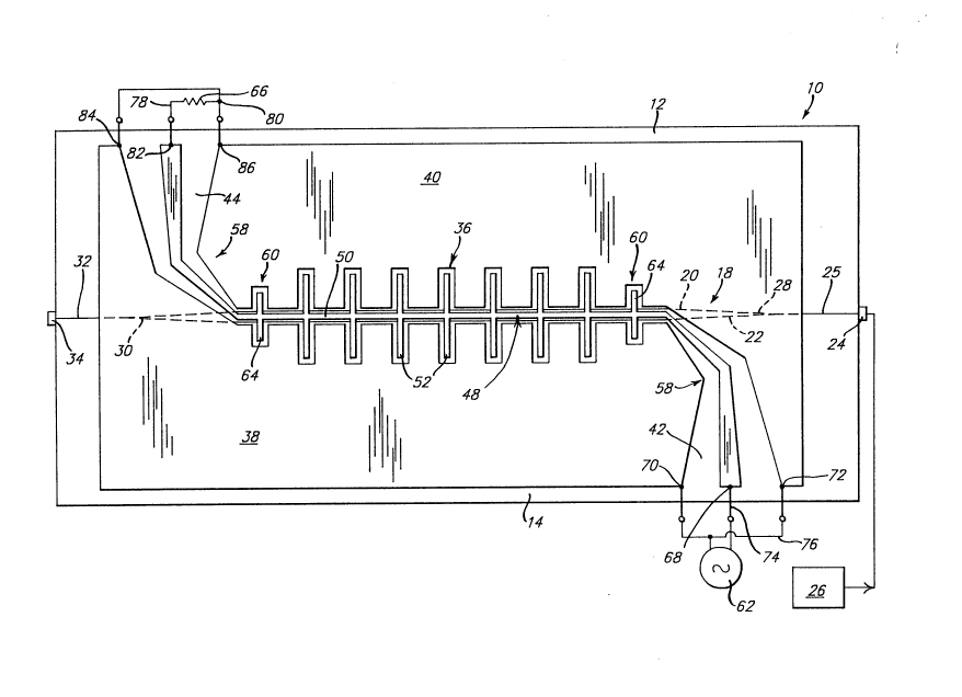
FIG. 1 is a top view of an electro-optic modulator
made in accordance with the teachings of this invention;
FIG. 2 is a partial enlarged top view of the
modulator shown in FIG. 1; and
2 G ~
1 FIG. 3 is a partial cross-sectional view taken along
the lines 3-3 of FIG. 2.
DETAILED DESCRIPTION OF THE PREFERRED EMBODIMENT
Turning now to the drawings, the electro-optic
modulator 10 is formed on a substrate 12 having a major
surface 14. Preferably, substrate 12 is formed of X-cut
lithium niobate (LiNbO3). The term "X-cut" refers to a
particular crystallographic orientation of the substrate
material, which is determined by industry standards. The
use of X-cut lithium niobate substrates are advantageous
over the known use of Z-cut lithium niobate substrates.
The use of Z-cut lithium niobate substrates generally
requires that the RF electrodes be placed vertically above
the optical waveguide. This, in turn, usually
necessitates the use of a silicon dioxide (Sio2) buffer
layer to prevent optical loss. However, this buffer layer
can be a source of bias instability. The use of X-cut
lithium niobate alleviates these problems because it
requires no buffer layer. The optical waveguide can be
placed between the metallic electrodes of the RF coplanar
waveguide as used in this invention.
The optical waveguide 18 is patterned into a
Mach-Zender interferometer. Optical waveguide 18 includes
at least two generally parallel optical waveguide channels
20 and 22 which are formed in the substrate 12 immediately
underneath major surface 14 as can be seen most clearly in
FIG. 3. In this embodiment, the waveguide 18 includes an
input 24 coupled to light source 26 such as a laser.
The waveguide 18 can be formed by diffusing
titanium into the surface 14 of substrate 12 using well
known techniques. The diffused titanium generally takes
the form of a strip 25 which splits at junction 28 into
the two channels 20 and 22. The channels 20 and 22 run
parallel to each other throughout a substantial length of
the substrate 12 and then are again joined together at
-- 2~2~3~7
1 junction 30 to form a line 32 terminating at optical
output 34. The optical output 34 typically is coupled to
an optical fiber, which serves as the transmission link to
an optical receiver.
The electro-optic modulator lO includes a
symmetrical RF coplanar waveguide 36. The RF coplanar
waveguide 36 generates an RF electric field in a region 46
between two metallic ground planes 38 and 40 on the major
surface 14 of the substrate lO. Waveguide 36 has openings
10 42 and 44 on opposite sides of the substrate 12. In the
preferred embodiment, opening 42 is an input opening
coupled to an RF source 62.- Opening 44 is an output
opening coupled to an RF load 66.
Centrally located within the region 46 and upon
the major surface 14 is a phase regulating conductor 48 of
the intermittent interaction type. The major length of
conductor 48 is in the form of a strip 50 having stubs 52
oriented transversely along both sides of the strip 50.
Turning to FIG. 2, the length (L) of the stubs 52 and
periodic distance (d) between the stubs 52 are determined
by the following relationship:
fD d (Nm ~ No)= -c (2L/~ + n)
where L is the length of the stubs, d is the length of the
periodic electrode section, fD is the RF design frequency,
~ is the RF design wavelength, c is the free space speed
of light, and n is an integer restricted to lie between:
fD d (Nm No)/
The edges of the RF coplanar ground plane conductors 38,
40 and the phase regulating conductor 48 define gaps 54
and 56, respectively.
2~263~7
1 Unlike prior electrodes of the intermittent
interaction type, the phase regulating conductor 48 is
symmetric about the axis of RF propagation. This symmetry
causes the modulator to behave like a balanced
transmission line, and facilitates testing and packaging
of the modulator.
One of the features of the invention is the
incorporation of impedance transforming circuitry 58 and
impedance matching features 60 within the modulator 10.
10 Having impedance transforming and impedance matching
characteristics built into the modulator 10 facilitates
connection of the RF source 62 since no extra impedance
matching circuitry is required. Impedance transforming is
performed by tapered input and output openings 42 and 44.
15 The impedance matching is carried out by end stubs 64
- which are shorter than the middle stubs 52. Together the
impedance transforming openings 42, 44, 58 and the
impedance matching stubs 64 transform the modulator's RF
impedance to the impedance level of the source and the
20 load. The impedance matching stubs 64 serve to transform
the impedance of the periodic electrode structure to the
impedance of an unperturbed linear RF coplanar waveguide.
The impedance transforming sections 58 serve to bring the
impedance level seen by the RF signal at a location just
25 outside the impedance matching stub up to the impedance
level of the source and the load.
The RF coplanar waveguide 36 and phase
regulating conductor 48 can be formed by first depositing
a layer of conducting material upon the major surface 14
30 of substrate 10. This may be accomplished by thermal
deposition o. sputtering of the desired metal onto the
substrate in a vacuum chamber. In the preferred
embodiment, gold is used with an underlying layer of
chromium or titanium to facilitate adhesion to the major
35 surface 14 of substrate 12. The metallic ground
conducting layers 38, 40 and the phase regulating
2~2~37
1 conductor 48 are up-plated in thickness using an
electrolytic gold plating solution and the gaps 54 and 56
are etched by an iodine gold etchant and a buffered oxide
etch (containing hydrofluoric acid).
The connection of the microwave source 62 and
the load 66 to the modulator 10 is straightforward.
In the preferred embodiment, a terminal 68 is connected to
one line 74 from the source 62, while terminals 70 and 72
are connected to the other line 76 of source 62. One side
78 of load 66 is connected to terminal 82, while the other
side 80 is connected to terminals 84 and 86.
The method for modulating an optical signal
begins with passing an optical signal of a given phase
from optical source 26 through optical input means 24 into
the optical waveguide 18 of the modulator. The signal
enters both channels 20 and 22. Next, the coplanar
waveguide 36 is coupled to a modulating RF signal source
62. The electric field components in the gaps 54 and 56
are oriented generally perpendicular to the direction of
RF signal propagation and are of opposite polarity. In
the area of the optical waveguide channels 20 and 22, the
electric field components pass through the channels and
electro-optically change their waveguide indices and,
therefore, the phase of the optical signals. Since the
phase changes within the channels 20 and 22 are different,
amplitude modulation occurs at the junction 30 when the
optical signals in channels 20 and 22 combine.
Since the RF signal velocity is less than the
optical signal velocity, the electro-optic modulator 10
incorporates the phase regulating conductor 48. The phase
of the microwave signal in the coplanar waveguide 42 is
periodically advanced by removing the signals in the gaps
56 and 54 from the area of channels 20 and 22 and passing
them around stubs 52. When the signals return to the area
of the channels 20 and 22, the microwave and optical
signals are again in phase. This electrode structure
2~2~33~;7
.
1 makes possible the modulation of optical signals by RF
signals above microwave frequencies. The RF source output
power needed to achieve sufficient depth of modulation can
be reduced by increasing the length of the modulator.
Although the invention has been described with
particular reference to certain preferred embodiments
thereof, variations and modifications can be effected
within the spirit and scope of the following claims.