Note: Descriptions are shown in the official language in which they were submitted.
2 ~
This invention relates to transmitters and
particularly to small, low voltage (1~5 to 6 volts nominal)
transmitters ~or transmitting at a single selected frequency,
normally (but not essentially) at a very high ~requency
(VHF), that is greater than 30 MHz.
In the design of transmit~ers which are used for the
location or tracking of birds, animals, vehicles, people or
other objects it is desirable to use as small and light a
transmitter as is possible.
The invention is particulary concerned with
transmitters Eor use in the sport of falconry. For such
sport it is common for small transmitters to be attached to
hunti.ng birds in order that they can be tracked and located
if lost or ou-t of sight. For this use it is particularly
important that the transmitters are small and light while
; remaining capable of emitting as strong a signal as possible.
It is also desirable that their active life is of several
days (at least four).
The frequencies used for this sport are designated in
each country in which it is praticed. In the UK the legal
frequency gran-ted by the government is approximately 173-17~
MHz. In USA, Canada, Europe and the Middle East -the
frequency alloted for falconry is approximately 216 M~lz. In
Germany frequencies of 151 to 155 MH~ and 403 to 405 MHz are
also used.
The transmitter clrcuit ls usually based on a crystal
oscillator having a predetermined nominal frequency, a
Erequency multi.plylng and arnpliying circuit and a pulsing
circuit desiyned to give a puLsed output at -the predetermi.ned
frequency. The transmitters normally have a power less than
S~ mi.lli.watts and are driven by batteries at 3 or 4OS volts
nominal.
The transmit~er ci.rcuit most comrnonly used at present
.: :: ... .,. ,. : : - . ,.:. . :, ~ -
..
2 2 J~
in falconry i5 that shown in Fig. 6. In this circuit the
crystal oscillator stage O oscillates at a frequency
approximately one third that required (216 MHz) and a
frequency multlplying circuit stage M is arranged to triple
the frequency. This known circuit has a pulsing stage P
providing an OFF period in which no signal is transmitted and
an ON period in which a signal is transmitted. The OFF
period is defined basically by a capaci-tor charging up
through a resistor and the ON period by -the same capacitor
discharging through another resistor and a translstor which
forms part of the oscillator stage. For this known circuit
to function correctly a good DC gain characteris-tic is
required for the transistor. For efficient oscillation,
however, that transistor also needs to have a good gain
characteristic at the crystal frequency. These requirements
are often conflicting and the result is a wide amptitude
variation of output signal from the oscillator stage and thus
from the transmitter. The frequency tripling s-tage,
mentioned above, is chosen so tha-t -the oscillator stage can
function at a lower frequency where it is possible to obtain
transistors with a sufficient DC gain to operate the pulsing
circuit, but this is less efficient than, for example, a
frequenc~ doubling circuit. There is no means for tuning the
frequency once assembled.
An object of the present invention is -to provide a
more efficient transmitter circuit which will provide a
higher output power for less battery power, which is small
and light and which is preferably reproducable from one
e~ample to another using standard components.
Accordingly, the present invention provides a low
voltage, single frequency, transmitter circuit comprising an
oscilla-tor stage including a crystal oscillator having a
predetermined nominal frequency and a first -transistor, a
frequency rnultiplying and amplifying stage arranged to
.: :~ - ; :
.:
~2~
multiply and amplify said nominal frequency, and a pulsing
stage, characterised in -that
the frequency multiplying circuit is arranged
preferably to double the frequency, and
the pulsing stage comprises at least a second
transistor distinct from -the first transistor, which second
transistor is switched off duriny an OFF period when there is
no output and is switched on during an ON period and in which
the O~F to ON period is in the ratio at least 15:1 preferably
20:1.
This gives greater efficiency and minimises the
current drawn. Preferably the on pulse width is in the range
40 to 70 millisec.
Preferably the pulsing circuit comprises two
transistors each of which is switched off during the OFF
period. Alternatively a unijunction transistor is used.
Preferably these have effective negative resistance and
therefore a fast action. This gives a sharp narrow pulse.
With advantage the oscillator circuit includes a
tuning means, preferably a variable capacitor, by which the
tolerances of the crystal frequency and other components of
the oscillator stage can be compensated. ~his allows the
frequency to be accurately adjusted after assembly so that
each transmitter made from standard components has the
required frequency. Also it allows the output for the
oscillator circuit to be ma~imised.
The output from the at least second transistor of the
pulsing stage is connected to the crystal oscillator via a
resistor whose value is selected to cover all variations of
the gain specification of the translstor of the oscillator
circuit. The transistor of -the amplifying stage is
preferably biased on.
~ he components forming the frequency multiplying and
amplifyiny staye also have tolerances which separa-tely
introduce inaccuracies in the output Erequency compared with
the required nominal frequency. Preferably this circuit also
includes tuning means, distinct from the tuning means in the
: ~ . . ..
- . . : , . ~: :
. : , ., ~ : ,
.. , , :
:: ; . , :.............. ,
2~2~
,, .
oscillating circuit, whereby the final desired frequency of
the amplifier circuit can be -tuned to compensate for
component tolerances thus causing the output power and the
efficiency to be maximised.
Another important aspect of the circuit which may be
claimed independently is that the transmitter is directly
connected to an antenna, without the use of an intervening
transmission line, and the output impedance of the amplifier
stage is matched to the antenna impedance in the range 10-30
ohms.
, Preferably the voltage variation in the pulsing
circuit is in the range 1/3 to 2/3 the supply voltage -1- or -
20%.
The embodiments of circuit described by way of example
; ~ 15 are provided on a circuit board of 12-15mm length and 8mm
wide, located in a casing of less than 2500 cu mm volume with
-the whole transmitter weighing~less than 7 grams.
::
~: :
Embodiments of transmitter circuit with antenna and
casing, ln accorda~nce with the invention, will now be
described, by way of example only, with reference to the
accompanying drawings of which :-
Figure 1 is a exploded side view of the parts of a
transmitter and antenna ready for assembly,
Figure 2 is a sectional view of the parts assembled
Figu~re 3 is a diagram of one embodiment of transmitter
circuit,
Figure ~ is a diagram of an alternative form of transmitter
circuit,
~igure 5 is a diagram of a further alternative form of
3~ transmikter circuit, and
Figure 6 is a circuit diagram of a prior art transmitter
circuit.
. , ,:
:~ . : : :. .. . : . .
`: :
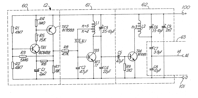
The transmitter circuit 12 is located on a printed
circuit board 13 having an output terminal 14 to which the
antenna 15 comprising a colled section 16 and a straight wire
portion 17 is connected. The transmitter has a casing
comprising an aluminium cylindrical body 18 and a cap 20.
The body is open at one end the exterior surface oE which is
threaded at 21 and the cap is 1nternally threaded at 22 to
screw over the open end. The base of the body 18 is formed
,
with a central circular aperture 23 through which the antenna
projects. The transmitter casing for example is of length
27 rnm and external diameter 10 mm. The transmitter has
,; additionally an insulating sleeve 24, an insulat~ng washer 25
and a battery connector 26 which comprises a stud 27
extending through the washer and defining a slot into which
the end of the printed circuit board is pushed. Three
batteries 30, each of 1.5 volts nominal, are located in ~he
casing between the battery connector and the end of the cap
and~are surrounded by the insulating sleeve 24.
To assemble the transmitterj with the antenna
connected to the printed circuit board, the circuit board is
slid into the body ~18 of the casing until it is fully against
the base of the body. The insulating sleeve 24 is then slid
against the washer 25 to cover the inside of the body ~or the
length of the battery compartment. Five layers 31, 32, 33,
34, 35 of insulating heat shrink material are then placed
over the antenna coil portion 16 and the base of the body 18
starting with the smallest first, as seen in figure 2. These
may include adhesive. The batteries are located in the
battery compartment and the cap is screwed onto the casing
body. The whole transmitter, casing and batteries, may be
made to weigh as little as 7 grams and have a volume less
than 2500 cu mm.
In this example the transmitter had a frequency o~
216.1 MHz, and an output impedance of approx 22 ohms (10 to
30) to match the antenna radiation resistance. The coiled
:`l
ç
wire portion of the antenna had the following dimensions: 29
turNs of enamalled copper wire 0.56 mm diameter, lS mm
length, an internal dimension of 3.5 mm diameter (an
inductance of about 700 nH). The straight wire was made of
7/0.2 mm stainless steel cable, having a 185 mm length. The
capacitance of the wire at this frequency is approximately
2.5 pF. The straight wire portion can be made from steel or
copper or alloys of these and can be twisted or solid and
insulated or not. The electrical length of the coiled wire
portion was approx. 52 (Theoretical split 22 for the
straight wire and 30 for the transmitter casing).
The first embodiment of transmitter circuit, as seen
in Figure 3, is designed to transmit at 216.1 MHz. The
circuit has positive and negati~e terminals 100, 101
respectively at 4.5 volts nominal and zero voltage, the
terminals being connected through the battery connector to
the katteries 30. Resistors Rl and R2, both 4M7, are
connected in series between the terminals 100, 101. Resistor
R4, lM0 has one end connnected to terminal 100 and the other
end~connected to one end of a resistor R5, 15K, the other end
of which is connected to the collector of a transistor TRl,
BC 848B, the base of which is connected to the junction of Rl
and R2 and the emitter of which is connected through
capacitor Cl, ~2 ~ 2), to terminal 101. The transistor TR2,
BC858B, has its collector connected to terminal 101, its base
connected to the junction of R4 and R5 and its emitter
connected via a resistor R7, 18K, to the terminal 101. A
resistor R3, 5N6, is connected between the junction of Rl and
R2 and the junction of R7 and the emitter of TR2. A
resistor R6, 820K is connected between the ]unction of R7 and
TR2 and the junction of Cl and TRl. The value of this
resistor will vary dependent on the voltage of the batteries.
In a modified version having only 3 volts of power R6 would
be 680 K. A crystal XLl having a natural frequency of
approximately 108 MHz has one side connected through a
capacitor C2, 47 pF, to the terminal 101 and the other side
connected to an intermediate point of an inductance Ll one
:~ : . :.: . ,
7 ~ ~ 2 ~
side of which is connected to terminal 100 and the other end
of which is connected to the collector of a transistor TR3,
BFS17. The emitter of TR3 is connected to the terminal 101
and its base is connected to the junction of crystal XL1 and
C2, this junction also being connected via a resistor R8,
47K, to the junction of R7 and transistor TR2. A variable
capacitor C3, (2.5 to 10 pF) has one side connected to
terminal 100 and the other side connected via a capacitor C4,
22 pF, to the terminal 101 and also to the junction of L1 and
TR3. The transistor TR4, BFR 93, has its emitter connected
to terminal 101, its base connected via a resistor R9, 2K2 to
~ terminal 101 and also via a capacitor C5, 47 pF, to the
! junction of C3 and C4 and its collector connected to an
intermediate point of an inductance L2. The inductance L2
has one end connected to terminal 101 and the other end
connected via a variable capacitor C6, 2.5 to 10 pF, to
terminal 100 and also via capacitor C7, 3.9 pF, and
capacitor C8, 10 pF, in series to the terminal 101.
Capacitor C9, (2N2), acting as a radio frequency decoupler
extends between the terminals 100, 101 and the output
terminal 14 of the transmitter is connected to the junction
between capacitors C7 and C8.
Each of the inductancies L1 and L2 comprises a powder
~ iron toroidal core with 0.1 mm enamel copper wire winding.
- 25 Inductance L1 has its intermediate point connected to the
crystal XL1 having 5 turns on the side connected to terminal
100 compared with 4 turns connected to transistor TR3.
Inductance L2 has its intermediate point connected to TR4
with 3 turns on either side.
The transmitter circuit consists of four basic
stages - a pulsing stage 60, an oscillator stage 61, a
frequency doubler and amplifier stage 62, and an antenna AE
matching circuit 63.
The pulsing circuit consists of TR1 and TR2 and
associated components. TR1 and TR2 are a complementary pair
and are both either conducting or switched off. When
conductive the voltage on the base of TR1 is approximately
2/3 the supply voltage VS, because R3 is in parallel with R1.
C1 is charging up -towards VS through R3 and TR2. When the
voltage at the emitter of TR1 is similar to that at its base,
TR1 and TR2 both switch off. The voltage at the base of TR1
5 is now about 1/3 VS because R3 is now in parallel (through
R7) with R2. C1 discharges through R6 towards 0 volts. When
the voltage at the emitter of TR1 falls to about 1/3 VS, TR1
switches on again and the action is repeated. The active
area of voltage variation is between 1/3 and 2/3 VS (+ or -
20%) and the potential divider R1, R2, R3 is ~ade up of high
value resistors (greater than 100K and preferably greater
than 800K) compared ~ith the value of R5 and R7 (ratio >10).
This reduces the current drawn from the batteries and
contributes to their longer life by increasing the linearity
of the charge rate and isolating the sagging effects of the
voltage supply caused by the pulsiny. Preferably R1, R2 and
R5 have similar values. The timing is determined by Cl in
combination with R5 and R6. C1 and R5 basically determine
the ON period, and C1 and R6 determine the OFF period. Both
2~ TR1 and TR2 are switched off during the OFF period thus
minimising the total current drawn. Preferably the circuit
is arranged to have a pulse length (ON time) of about 50
milliseconds (+ or - 20~) with a 20:1 off/on ratio (~ or -
20~)-
With the separate pulsing circuit of this invention,
having two transistors each independent of the oscillator
stage transistor, the oscillator transistor can be chosen for
efficiency at the crystal frequency. This allows both higher
efficiency in the oscillator stage and flexibilty in the
ON/OFF ratios. Varying R5 to change the ON time has little
efect on the OFF time and varying R6 to change the OFF time
has little effect on the ON time so the ratio o~ OFF and ON
times can be selected up to about 100:1. Preferably the
oscillator circuit is located on one side of the circuit
board and the pulsing circuit on the other side.
The crystal oscillator is based on the "Pierce
Harmonic" circuit. This circuit oscillates at half the
:: .
~,
:. : :: : . - ,
,: , :~. : ,.
.: - , :: -
- 2~3~
,~
required output frequency of the transmitter. L1 and C3 form
a tuned circuit and the feedback, via XL1, is taken from a
tapping on L1. C3 being a variable capacitor allows tuning
of the circuit to tune out the tolerances of the crystal and
more particularly tolerancies in L1. This achieves ability to
accurately set the frequency and maximum efficiency. Each
model can be tuned to the desired frequency using standard
componentsO
By comparison the prior art design of Fig 5 does not
have an ability to tune at this stage and the feedback is
taken from the junction of two series capacitors forming the
tuned circuit with an inductor.
The frequency doubler and amplifier stage 62 includes
the circuit around transistor TR4 and has the two functions
of frequency doubling and amplifying the ou~put. ~2 and C6
form a tuned circuit at the final desired frequency and
select the second harmonic of the signal presented to TR4.
This stage is tuned by variable capacitor C6 in order to take
out the tolerances of the components (in this stage), and
thus achieve maximum efficiency.
In order to achiev~e antenna matching, the output
impedance of the first amplifier stage is adjusted by the
ratio of C7 and C8 so as to match the antenna impedance.
With the desîgn o~ this invention the output impedance is
required to be matched to the antenna impedance and the
antenna is effectively tuned to compensate for the lack of a
good ground plane. In known designs the antenna is taken
directly from the output tuned circuit. This is a relatively
high impedance but in the absence of a good ground plane,
this gives a better overall radiated power than matching to
the normal quarter wavelength antenna.
The transmitter circuit thus contains two separate
tuning systems. The capacitor C3 can be varied to tune the
crystal to the exact required frequency to take out the
tolerances of the crystal oscillator circuit. The capacitor
C6 can be varied thereafter for fine -tuning to take out the
tolerances of the components in the multiplying and
-, ~ :
- - ,:
amplifying stage.
A modified ~ransmitter circuit is shown in Figure 4.
This is substantially the same in operation as the circuit of
Figure 3 and like parts have been given like reference
S numerals and will not be redescribed.
The pulsing stage of the Figure 4 circuit has been
achieved with fewer parts, namely only 4 resistors 2
transistors and 1 capacitor, allowing the size of the circuit
to be reduced.
In this modified pulsing circuit, a resistor Rll
(lM2) and a capacitor Cll (1 ~ F) are arranged in series
between positive and negative voltage sources 100, 101.
Transistors TRll and T~12 (respectively BC858B and BC848B)
have been arranged as a four layer semiconducting device
known as a Unijunction Transistor which has effective
negative resistanceO TRll and TR12 are connected as shown
between the junction of Rll and Cll and the junction of
resistors R13 (2K2) and R14 (lOK) which are connected in
series between 100 and 101.
The emitter of TR12 is connected through R15
(20K) to the crystal oscillator and through R16 (lOK) to the
base of transistor TR4. The value of R15 has been chosen to
cover all variations of the gain specification of the
transistor TR3.
When the circuit is switched on the capacitor Cll
charges through resistor Rll and when the emitter potential
of TRll becomes higher than its base potential transistor
TRll starts to conduct. In so doing the collector of TRll
endeavours to rise towards the emitter potential and turns
the base of transistor lrRl2 positive which causes it to
conduct. When TR12 starts to conduct it turns the base of
TRll negative so setting up a regenerative action.
Capacitor Cll then discharges through resistors R15 and R16.
The combination of transistors TRll and TR12 thus provide a
fast acting switch with the point of switching set by the
ratio of R13 and R14. The OFF time while Cll is charging up
is dictated by the values of Rll and Cll and the ON time when
, ~
11 2~2~
Cll is discharging through R15 and R16 is determined by the
values of Cll and R15 and R16.
The positive pulse produced by charging of Cll
through Rll starts the oscillator and puts a bias on the
transistor TR4 of the amplifier circuit. Because of the
effect of a negative resistance of the transistor combination
TRll and TR12 the switch action is fast acting producing a
narrow steep sided positive pulse, for e~ample having a width
of 40 to 70 ~illisecs.
The antenna matching circuit C7 (3p9) and C8 (lOp) is
now connected to the line 100 and C9 replacd by C10 (4n7).
A further modified transmitter circuit is shown in
Figure 5, this being essentially a combination of the pulsing
circuit of Figure 3 with the oscillator stage, amplifying and
multiplying stage and antenna matching stage of Figure 4 with
variations and with different component values. Where the
function is essentially the same as in the previous circuits
this will not be described again.
In the pulsing circuit resistors R21 to R28 function
similarly to resistors Rl to R8 and have the values R21 820K,
R22 lM2, R23 lM2, R24 lM2, R25 47K, R6 1~2, R7 18K~ and R8
47K. This has the same reduced current usage advantage as
the Figure 3 circuit.
In the amplifying and multiplying stage R29 of 18K
replaces R9 and is connected between the base of TR4 and the
junction of R23 and R26. This acts to slighty bias the base
of TR4 on so that it acts as a class A amplifier instead of a
class C (se]f biased) amplifier as in the Fiyure 3 circuit.
This increases the second order distortion effect. C4, C5
have been replaced by C24 and C25 (each 33pF) in series with
each other between C3 and terminal 101, with the base of TR4
connected between the junction of C24 and C25. C23 (4n7)
connected between terminals 100, 101 provides an additional
radio frequency decoupler in the oscillating stage.
Transistor TR3 is of type BFR92A and transistor TR4
is of -type BFR92, 92A or 93 having a DC current gain in the
range ~0-200. This provides more reliable switching with the
,:
.:
, :. . : ................................. .. ..
.. . . ~ ... .. .
12
circuit values (R8 greater than 30K) required for achieving
the required short pulse.
The output stage is the same as that for Figure 4.
A transmitter in accordance with these circuits used
with 4.5 volts nominal batteries has been found to transmit
for seven days, as compared with about thirty six hours for
the prior art circult of Figure 6, and at a greater radiated
output power.
': ~ ; '
.