Note: Descriptions are shown in the official language in which they were submitted.
2~2~3~
BACKGROUND OF THE INVENTIO~
The present invention is directed to a measuring position for
a microwave component, having a carrier for the microwave component
and at least one test probe. The present invention is directed to
an arrangement for measuring both analog-le as well as digital,
hybrid or monolithically constructed circuits in quasi-planar line
technology having carrier materials (substrates) with an optimally
small surface. For example, single semiconductor components such
as, for example, housed or unhoused transistors, for example
MESFETs, have a small surface, as do components such as hybridly
constructed or monolithically integrated microwave circuits (MMIC)
or combined arrangements such as chip-carrier structures.
In the prior art, the measurement of housed transistors has
been performed with suitable measuring receptacl0s wherein the
terminal bands of the transistors are contacted via planar line
structures. Unhoused transistors have hitherto been tested in
measuring mounts with a web. Due to the irreversible contacting
by bond wire and solder, this measuring method is not non-
destructive. Therefore, the measured transistors can generally
not be re-used. The measurement of complete, monolithically
integrated circuits of GaAs material likewise has the disadvantages
recited for the measurement of unhoused transistors. This
measurement is not non-destructive and i~ complex and is therefore
suited neither for measuring individual components nor for
measuring a great number of elements as necessary in the final
testing during the manufacture of components.
There is a measuring position (Cascade Microtech, Inc.) for
measuring planar circuits on a semiconductor wafer. This measuring
position is equipped with test probes in coplanar line technology.
The measurement of a component with this type of measuring probe
requires a terminal configuration on the component in coplanar line
2 ~ 6 9
technology (without base metallization) or requires through-
contactings on the semiconductor wafer. A measurement of
individual integrated circuits on the chip level or on the chip-
carrier level with such a measuring position is only ~ossible with
additional measures.
SUMMARY OF THE INVENTION
The object of the present invention is to provide a measuring
position for a microwave component, having a carrier for the
microwave component and at least one test probe. It permits non-
destructive identification of the properties of microwave circuits
.... . . . . . .
on optimally small substrate areas even for the measurement of
quasi-planar circuits with connecting lines in asymmetrical
microstrip line technology.
This object is inventively achieved by a measuring position
wherein spatial positions of the test probe are variable and
adjustable in three spatial directions relative to the spatial
position of the carrier.
The spatial position of the carrier can be variable and
adjustable in three spatial directions or the spatial position of
the test probe can be variable and adjustable in three spatial
directions. A means for automatic adjustment of the carrier and/or
the test probe can be provided.
The test probe can be a coaxial line and a coaxial outer
conductor of the coaxial line can press against the carrier.
The test probe can be designed to exer~ a mechanical pressure
onto the microwave component. In one embvdiment the test probe is
rotatably seated via a hinge or joint. Furthermorel the test
probes can be chronologically movable in arbitrary combinations.
A means for direct testing of a semiconductor component can be
provided within a microwave circuit. The test probe can have a
multi-conductor structure. An integration of a network into the
est probe can also be provided.
A measuring position of the present invention makes it
possible that the dimensions of the circuits to be measured
(dimensions of the substrate, dimensions of the semiconductor chi~,
dimensions of the chip carrier, etc.) for the measurement are
limited in the direction toward low values only by the cross-
sectional dimensions of the test probes employed.
The electromagneti~ stray field, the emitted power and, thus,
the electromagnetic coupling of the aperture fields is essentially
defined by the cross-sectional dimensions of the test probes in
comparison to the wavelength of the fundamental wave on the lines.
The present invention makes it possible to use coaxial line test
probes having an inside diameter of the outer conductor of less
than O.7 mm. Such values lead to an allowable, minimum distance
of the apertures of the employed test probes of less than 1 mm,
which defines the minimally allowable substrate surface in the
measurement. A further miniaturization of the overall measuring
arrangement as well as of the possible test subject can be carried
out, so that spacings can be realized that allow a direct
measurement of MMICs or of transistors.
BRIEF DESCRIPTION OF T~E DRAWINGS
The features of the present invention which are believed to
~e novel, are set forth with particularity in the appended claims.
The invention, together with further objects and advantages, may
best be understood by reference to the following description taken
in conjunction with the accompanying drawings, in the several
Figures in which like reference numerals identify like elements,
and in which:
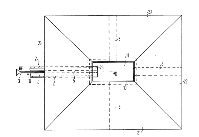
FIG. 1 shows a plan view of a four gate ~easuring mount;
FIG. 2 shows a partial section through a measuring mount of
FIG. l;
~2~9
FIG. 3 shows a cross-section through a part of a measuring
mount;
FIG. 4 shows a section through a part of a measuring mount;
FIG. 5 shows a section through a part of a measuring mount;
FIG. 6 depicts the aperture region of the coaxial line test
probe for test subjects having coplanar connecting lines;
FIG. 7 shows a microstrip line test probe;
FIG. 8 shows a cross-section through a shielded double line
system;
FIG. 9 shows a cross-section through a planar multi-
conductor structure;
FIG. 10 shows a conductor structure of an adapted test
probe; and
FIG. 11 shows a longitudinal section through a filter or
matching network in coaxial line technology.
DESCRIPTION OF THE PREFERRED EMBODIMENT
FIG. 1 shows a plan view (fundamental arrangement) of a four-
gate measuring mount including coaxial line-to-microstrip line
junctions. In the center of the measuring mount, FIG. 1 shows the
test subject (without an overhead conductor) with the substrate 11
that is connected to a measuring system of a conventional type, for
example HP 8410/8510, via coaxial lines 5 (DC and RF~ or test
probes 5 (DC).
Using coaxial lines for the test probes 5, these coaxial lines
comprise an outer conductor 2, an inner conductor 3 and a
dielectric between outer conductor 2 and inner conductor 3, for
example Teflon 4. Dependent on the application, the test probes
5 have DC or RF feeds 6.
The test probe~ 5 serve the purpose of contacting test
subjects having lines in coplanar and asymmetrical line technology
whose miniaturization is enabled by the present invention. A
2~2~3~9
~easuring position of the pres~nt invention fundamentally has a
bipartite type mechanical structure and enables the automatic
adjustment of the overall arrangement.
Among other things, miniaturized, open coaxial lines, for
example solid jacket cables, are used as test probes 5. At their
open end, these coaxial lines can have a nose 25, or only the inner
conductor 3 can be conducted out of the coaxial line, so that
either the nose 25 or the inner conductor 3 overlaps the surface
of the substrate 11 in the plan view of FIG. 1. The nose 25 can
be composed completely of Teflon 4 or the nose 25 can comprise a
part of the outer conductor 2 and a part of the Teflon 4.
Structural details of the mechanical part of the measuring
mount may be seen in FIGS. 2 through 5. With a design of the
present invention, there is fundamentally the possibility of
measuring circuits in microstrip line technology whose area is on
the order of magnitude of the chip carrier arrangements to be
tested. Such chip carrier arrangements can have dimensions of
approximately 2 x 5 mm2. In a measurement of the present invention,
the circuits are neither modified nor destroyed, so that they are
available for the intended use after the testing (non-destructive
measurement in the microwave range). It is thus not only possible
to make spot checks of production batches, but it is possible ~o
test any manufactured circuit that is to be used. FIGS. 2
through 5 each respectively show at least a part of the cross
section of a measuring arrange~ent of FIG. 1. In particular, FIGS.
2 through 5 illustrate the junction between the test probes and the
microstrip lines on the test subject. This junction can be
executed with a miniaturized coaxial line having a solid jacket.
A semi-rigid line can be used as the coaxial line, for example UT
34 having an inner conductor diameter of 0.200 mm and an inside
diameter o~ the outer conductor of 0. 66 mm. The inner conductor
2~26~9
~ is pressed onto the overhead conductor of the microstrip line on
a substrate 11 by the projecting nose 25 of outer conductor/Teflon.
The substrate 11 can be composed of Al203 ceramic having a thickness
of 10 mil and an overhead conductor width of a 50 ohm line of 0.248
mm. The outside of the coaxial outer conductor 2 can thereby lie
on the carrier base plate 10. The carrier base plate can be
composed of CuMoCu. The end faces in the aperture plane of the
open coaxial line thereby press flush against the edge of the
substrate 11.
The chip-carrier arrangement is held and adjusted by alignment
pins 9 in the back side of the carrier base plate 10. The carrier
base plate lo can be additionally fixed by a mount (carrier holder)
8. The carrier holder 8 can be composed of Teflon. Teflon is a
registered trademark. The miniaturized coaxial lines 5 have their
cross-sectional dimensions selected such that, first, an
electromagnetic coupling of the two aperture fields is prevented
on the basis of the relatively small substrate dimensions and such
that, a matching of the characteristic impedance and field line
pattern of the two line forms is guaranteed. The difference
between the radius of the inner conductor and the outer conductor
of the coaxial line should therefore approximately correspond to
the height of the substrate 11 in order to avoid additional
matching networks. The coaxial line 5 can be arranged at an angle
relative to the base area of the carrier in order to improve the
contact between microstrip lines and test probes.
A design inclined by an acute angle is suitable in order to
diminish the electromagnetic reactants of the walls of the
measuring mount. The surface of the measuring mount should thereby
be coated with a suitable attenuation material.
For inner conductors 3 having small cross-sectional
dimensions, the nose 25 or an additional mechanism, for example an
2~369
~lignment pin 9 or a holdsr 8 of dielectric material having low
permittivity is provided in order to guarantee the adjustment
needed for a reproducible contacting between test subject and test
probes. The test probes 5 whose nature and number can vary
depending on the test subject and contacting (DC and RF) are
mounted in common or individually on one or more mounts. The test
probes are seated resiliently and resist twisting in a longitudinal
direction. The transition from the test probes to the further
measuring system occurs on the basis of suitable coaxial
arrangements.
The significant stray field at the open end of the test probes
5 propagatas in a volume region whose radius corresponds to
approximately 2-3 times the inside radius of the outer conductor
2. The minimum distance of the test probes is defined as a
function of the position of the test probes relative to one
another. It is thereby respectively assumed that the wavelength
of the fundamental wave in the coaxial line 5 is far greater than
all cross-sectional dimensions and that the inner conductor or,
respectively, overhead conductor of the test probes has only such
a length, beyond the aperture plane of the test probe, that is
extremely small in comparison to the wavelength of the fundamental
wave in order to avoid additional emission in this region. This
condition, however, i5 always met given the intended application
of the measuring mount and in the planned frequency range up to 18
GHz and above 18 GHz, since the thickness of the substrate
approximately corresponds to the difference between inner conductor
radius and outer conductor radius of the coaxial line 5 in order
to guarantee a matching of resistance and field pattern in the
junction region between test subject and test probe. For solid
materials, the measuring arrangement can be miniaturized or,
respectively, enlarged proportionally to the operating fre~uency
3 ~ 9
(assuming no losses~ without influencing the properties of th~
arrangement. Only an approximately constant influencP of the
mechanical manufacturing tolerances thus must still be taken into
consideration.
The basis for a measuring position of the present invention
can ~e a conventional probe measuring position that is rebuilt in
the fashion of the present invention. A microscope can be used
with which the adjustment of the test subject, i.e. the adjustment
of the overhead conductor 26 on the test subject and the inner
conductor 12 of the coaxial line, can be checked. The horizontal
motion (x-z direction FIG. 2) occurs, for example, manually with
the assistance of a micrometer screw or occurs computer-controlled
via a corresponding support; the vertical (y-direction) motion
occurs with a suitable arrangement. Additionally, the coaxial
lines can be resiliently moved in a z-direction but protected
against twisting. The properties of the junction between coaxial
line 5 and microstrip line can thereby be improved. The contacting
of the test subject occurs in the RF or HF range and in the DC
range via the coaxial lines S or in the DC range via standard test
probes 5 insofar as these test probes 5 do not deteriorate the
function of the test subject. The measuring arrangement is
suitable for implemanting complete, error-corrected ("on carrierl',
'lon chipll calibration), vectorial measurements at circuits on an
op~imally small substrate surface.
FIG. 2 shows an anti-twist cable layout 17 having replaceable
cables. The replaceable cables are resiliently arranged in a
longitudinal direction. The measuring mount 15 has an alignment
pin 14 in order to provide a contact pressure of the coaxial inner
conductor 12 on the overhead conductor 26 of the substrate 11. The
measuring mount 15 has a damping material 16 on its surface. The
coaxial cable has a SMA connection 13 and the measuring arrangement
2~2~3~
of FIG. 2 has a platform 7.
FIG. 3 shows a cross section through a part of a measuring
mount similar to the measuring mount of FIG. 2. It can thereby be
clearly seen that the alignment pin 9 serves the purpose of
adjustirg che chip carrier 10. The measuring mount 27 has a
resistance layer 28 on its surface. The pressing mechanism 29, 30
that comprises an alignment pin 30 of, for example, Teflon and an
alignment pin 29 that is arranged inside the measuring mount 27,
serves the purpose of fixing the coaxial line 5 and of pressing the
roaxial inner conductor 12 of this coaxial line 5 onto the overhead
conductor metallization 26 on the substrate 11.
The arrangement of FIG. 3 has an upper part 33 and a lower
part 34. The upper part 33 is composed of the probe structure and
of the upper part of the measuring arrangement. The lower part 34
of the measuring arrangement is arranged on the platform 7 of the
probe measuring position.
In cross section, FIG. 4 shows a further possibility for a
junction between a coaxial line and a microstrip line. The coaxial
inner conductor 12 contacts the overhead conductor metalli~ation
26 on the substrate 11. The underside of the substrate 11 can have
a metallization 32. An electrical contact ~etween the substrate
11 and the outer conductor of the coaxial line is produced via the
outer conductor-to-ceramic contact 31.
FIG. 5 shows a further version of the pressing mechanism
between the test probe and the test subject. The inner conductor
12 and the outer conductor 43 of the coaxial line are pressed onto
the chip carrier arrangement 10, 11 in that the second part of the
measuring mount 39 is angularly arranged. This second part of the
measuring mount 39 is adjustably arranged in order to be able to
set the mechanical pressure of the coaxial line against the test
subject at the beyinning of a mea~urement. The chip carrier
2~2~
~rrangement 10, 11 is thereby resiliently seated in the direction
of the arrows 41. The first part of the measuring mount 40 is also
resiliently fashioned in the direction of the arrows 41. The first
part of the`measuring mount 40 and the second part of the measuring
mount 39 are provi~led with hinges or joints 42 at a suitable
location. The be~ding point thereby occurring between the first
part of the measuring mount 40 and the second part of the measuring
mount 39 is shown exaggerated in FIG. 5 in order to illustrate this
principle.
The pressing direction in which the coaxial line is pressed
against the test subject is referenced 35. A tensile direction 36
derives for the measuring arrangement of FIG. 5. The measuring
arrangement of FIG. 5 has a rotatable fastening 37 around which the
second part of the measuring mount 39 can be rotated in the
direction 38.
FIG. 6 shows the aperture region of coaxial test probes 5 when
the test subject comprises a connecting line in coplanar line
technology. The length L of the nose 25 can be variably adapted
to the respectiv~ test subject. The aperture region of coaxial
test probes is shown in FIGS. 2 through 5 for test subjects having
connecting leads in asymmetrical mi~rostrip line technology.
FIG. 7 shows the overall arrangement of a planarly constructed
test probe. This test probe is composed of a basic structure of
carrier material and base metallization 45 onto which a further
dielectric layer 44 with the upper conductor 46 is applied. The
overall structure of this test probe may be shielded under certain
circumstances by a further metallization 47. The overall structure
of the test probe can comprise a nose 25. The right-hand part of
FIG. 7 is a section through the center of the left-hand part of
FIG. 7. FIG. 7 shows a microstrip line test probe for test
subjects having connecting lines in asymmetrical mi~rostrip line
11
2~2~
technology. In modified form, such a microstrip line test probe
is also suitable for a test subject having connecting lines in
coplanar line technology.
For use of a test probe in microstrip line technology, the
junction to the measuring ~ys~em occurs via a suitable microstrip
line-to-coaxial line ju-nction. The test probes can be movably
~eated similar to the test probes of FIGS. 2 through 5.
Test probes can be manu~actured in coplanar or asymmetrical
microstrip line technology or in triplet technology with
respectively slight modification of the basic structure of FIG. 7.
Independent of use in the measuring arrangement, the test
probes are suitable ~or measuring integrated circuits on a chip
level that are firmly implemented in a hybrid constructed circuit.
As a result of the double line structure, these structures
can be used in a broad frequency range beginning with a frequency
of zero.
FIGS. 8 and 9 shows multi-conductor structures wherein the
test probes 5 comprise a plurality of inner conductors.
FIG. 8 shows a cross section through a shielded double line
system (three-conductor arrangement) having two inner conductors
47 and one outer conductor 48. FIG. 9 shows a cross section
(aperture region) through a planar multi-conductor structure having
a base metallization 49, a plurality of overhead conductors 50, a
shielding 51 and two dielectrics 52, 53.
FIGS. 10 and 11 show coaxial and planar filter structures.
Networks can be integrated into the test probes 5, for example, for
decoupling radio-~requency power, for matching, attenuation and
filtering of harmonics or the like. Corr~sponding networks can
also be applied on the test subject holder. FIG. 10 shows an
overhead conductor structure of an adapted test probe 5 with DC
blocking capacitor 54 and DC supply 55 in planar line technology.
12
2~3~9
~he arrow 56 points to the measuring system and the arrow 57 pOihts
to the test subject.
FIG. 9 shows schematically a longitudinal section through a
filter or matching n~twork in coaxial line technology. The test
probe of FIG. 11 has an inner conduct~or 12, an outer conductor 43
and a nose 25. The measuring arr~ngement of the present invention
can be composed of two parts for every junction between the test
subject and measuring mount, these two parts being connected to one
another via a hinge or joint (FIGS. 2 through 5). The first part
is composed of the test subject carrier that is the same for all
test probes and is composed of the further, lower part that is
movable in the three spatial directions (x, z; continuous motion;
y; two conditions).
The second part is composed of the mount for the respective
test probe and of the overall, upper part that is either
manufactured of a material that has optimally few reactances onto
the operating properties of the measuring arrangement or that is
coated with a suitable damping material.
The test probe i5 rigidly connected to the second part. The
base plate 10 of the test subject carrier has an electrical contact
with the base metallization 32 of the quasi-planar circuit on the
shortest path.
The mount 8 of the test subject carrier is composed of a
material whose properties have optimally few reactances onto the
operating behavior of the arrangement, for example of a dielectric
having a low value of ~he permittivity factor that is also coated
with a suitable damping or attenuation material. The te t subject
can be exactly fixed on the basis of additional measures such as,
for example, alignment pins 9 in the carrier base plate 10. The
test subject carrier is resiliently seated in order, first, to
gu2rantee an improved contacting of the junction between the test
13
~2~
subject and test probe and, second to guarantee a junction having
constant pressing power (spring constant). The test subject
carrier can be ~oved in the x-z plane and can also be moved in the
y-direction by computer-controlled with the ~ssistance of a
coordinate table, for example corresponding to ~n adjustment rule.
Respectively ons measuring mount 21 through 24 is movably
arranged with respect to the test ~ubject per test probe 5 in FIG.
1. In combination with the mobility of the test probes 5 in a
longitudinal direction of these test probes and via a further hinge
or joint in combination with the resilient holding of the test
probes and test subject, the movable seating of the two parts of
the measuring arrangement of the test probes 5 via a hinge or joint
at a location that does not influence the operating behavior of the
arrangement, guarantees optimum contacting in the region of the
junction of the test subject line and the respective test probes
5 in their aperture region on the basis of manual or automatic
motion of the arrangement in y-direction. A test subject line can
thereby be an asymmetrical microstrip line or a coplanar line
with/without base metalliæation. Over and above this, the
mechanically uncoupled allocation of the two parts of the measuring
arrangement is also possible. ~ath arrangements enable a
reproducible, fast and computer-controlled adjustment. A
microscope (manual adjustment) or an ~lectrical signal that can be
derived from the reflection or transmission behavior of the
circuit, from a reference structure in common on the test subject
or on the test subject holder or from the output signal of a
suitable, conventional means (automatic adju~tment) serves for
monitoring the adjustment of the inner conductor of the coaxial
line or, respectively, of the overhead conductor of planar test
probes on the overhead conductor of the planar line of the test
subject. This electrical signal need not necessarily be derived
14
`rom the behavior of a planar structure in the microwave range.
Optical or electronic means of a conventional type are also
suitable for this purpose. The refl~ction or, respectively,
transmission behavior of a microstrip line dependent on the
adjustment or on the excitation behavior of a resonant structure
can, for example, be utilized for this purpose in the microwave
region.
A measuring arrangement of the present invention can be part
of a conventional, computer-controlled measuring system for
identifying the analogue or digital electrical behavior of the test
subjects (for example, network analyzer, TDR measuring position,
noise measuring position or the like). This combination of
measuring system and mechanical measuring arrangement with
computer-controlled adjustment of the test subject permits non-
destructive, completely computer-controlled and error-corrected
(calibration method) measurement of quasi-planar circuits on small
substrate surfaces.
The present invention provides a reproducible contacting, low
wear of the test probes, automatic control of the adjustment
procedure for small cross sectional dimensions of the test probes
and for small overhead conductor width of the microstrip lines on
the test subject and also allows measuring events in a short time
period. Also in a manually implemented measurement the present
invention allows a fast changing of the test subjects and
employment in series measurement.
An automatic adjustment is advantageous for extremely small
widths of the overhead conductors (correspondingly low thicknesses
of the substrate 11).
Below a certain width of the overhead conductor of the test
subject, it is advantageous to use a test probe in planar
technology. The manufacturing tolerances of the coaxial test
2 ~ 3
probes, have a greater influence on the electrical behavior with
increasing miniaturization, characterized by the characteristic
line impedance and the wavelength constant of the fundamental wave.
Added thereto îs the behavior of the junction from the test probe
to the measuring system (voltage standing wave ratio on the line).
In the present invention, the contacting between test subjec'; and
test probe occurs either by the movement of the test probe, by the
movement of the test subject holder or by movements of the test
probe and the test subject holder in a bipartite arrangement per
test probe, this bipartite arrangement according to FIGS. 2 through
5 being mechanically coupled or mechanically uncoupled.
The test probes can comprise a nose 25. A pressing mechanism
provides adjustment of the coaxial inner conductor or,
respectively, of the overhead conductor of a planarly constructed
test probe. The contact pressure of the test probes against the
lines of the test subject can be very precisely defined, for
example by defined weights or spring constants that take affect at
a suitable location at the bipartite mechanism.
All test probes can be moved independently of one another,
can be moved in groups or can all be moved in common.
The test probes serve the purpose of contacting beginning at
zero frequency.
Conventional test probes as known from probe measuring
positions can alco be utilized in the measuring arrangement insofar
as they do not measurably influence the behavior of the circuit.
Independently of the employ~ent in the proposed measuring
arrangement, the test probes and their mounting and adjustment can
also be used for direct testing of integrated circuits and chip
arrangements within an overall circuit, for example GaAs chip
arrangements on through-contactings or chip carriers.
16
.9
A criterion for the automatic control of the adjus~tment
procedure and of the measuring procedure can be derived from the
measured signals at the test subject or at a reference subject.
The automated adjustment of the test subject or of the test probes
(separately or in common) derives therefrom. The reference
structure can be mounted on the test subject or on the holder of
the test subject. The control signal for moving the arrangement
can be acguired with optical or electronic networks or with
mechanical devices.
The present invention provides the contacting between the test
subject and test probe with the assistance of a bipartite
mechanical arrangement for every junction between test subject and
test probe.
The invention is not limited to the particular details of the
apparatus depicted and other modifications and applications are
contemplated. Certain other changes may be made in the above
described apparatus without departing from the true spirit and
scope of the invention herein involved. It is intended, therefore,
that the subject matter in the above depiction shall be interpreted
as illustrative and not in a limiting sens~.