Note: Descriptions are shown in the official language in which they were submitted.
2~26$12
.
1 --
SIG~AL-TO-~OISE RATIO INDICATI~G CIRCUIT
FOR FM RECEIVERS
Backqround
rrhe present invention relates in general to
identifying signal quality of a received radio
transmission, and more specifically to a stop circuit fQr
terminating a scan tuning operation when a transmission
is being received having a signal-to-noise ~atio greater
than a predetermined ratio. The present application is
related to U.S. application Serial No. (88-540) filed
concurrently herewith.
The measurement of received signal quality has
been employed in FM receivers for implementing a number
of different functions. For example, automatic scan
tuners which sweep through the FM broadcast band must
terminate a scan when a broadcast signal is receiYed
having a particular signal quality. Signal quality is
also measured in order to modify receiver characteristics
in response to certain conditions, e.g., output blanking
or reducing stereo separation in response to certain
kinds of noise. Signal quality may also be measured in
order to display a visual indication of recelved signal
quality to the user of the receiver.
Several different methods have been employed to
generate a stop signal for terminating the sweep
operation in an automatically scanning tuner. Most
methods rely on a quality measure based on the received
signal strength, or a frequency window determinsd by the
automatic freguency control (AFC) signal, or a
combination of both. Detecting the presence of a
received signal strength as being greater than a
predetermined magnitude is, by itself, a poor indicator
of signal quality. This is because the received signal
strength may be high while signal quality is low due to
., :
', ' ' : . '
.
-- 2
the presence of noise, adjacent channel interference, or
multipath interference. The use of a frequency window to
ensure that scanning is stopped accurately at the
frequency of a strong received signal does not eliminate
the possibility of stopping at a received signal
including noise and i~terference.
It is also known to e~amine the noise component
of a signal relative to the information signal component
in order to determine signal quality. For example,
communications transceiqers employ output inhibiting or
squelch when a particular level of noise is present.
However, the prior art systems measure noise at
frequencies that also contain information-related
components. Therefore, only noise that is substantially
equal to or greater than the information component can ~e
detected.
The measurement of the actual signal-to-noise
ratio of a received signal re~uires complicated and
; - e~pensive systems which can determine distinct power
values for d;fferent frequency ranges and generate a
ratio of the power values. Simplified systems are known
for FM receiver applications which measure the difference
in power values in-order to identiy a signal ~uality
level. For e~ample, Schiebelhuth et al, U.S. patent
3,889,192, describes a noise suppressing arrangement
which determines the absolute levels of the receiv~d
field strength and the receiver noise. The audio output
is enabled only when the field strength is above a
predetermined value and the noise is below another
predetermined value. Thus, whenever the audio output is
enabled, a received signal has at leas~ a minimum
signal-to-noise ratio. However, not all s;gnals having
that minimum signal-to-noise ratio will be accepted by
the system. For example, a signal having a field
strength slightly below the predetermined field strength
:, "- ,,
- . ,:
. . . . . .
-
. . ~. . : .
but having substantially no noise would result in the
audio output being inhibited. Similarly, a signal having
a noise component slightly in e~cess of the predetermined
noise value but having a very large field strength would
also not be output by the receiver.
Summar~ Qf the Invention
It is a principal object of the present
invention to detect the reception of an F~ signal having
a predetermined signal quality in a manner which is
relatively inexpensive and requires few components.
It is another object of the present invention to
provide apparatus and method for indicating the
signal-to-noise ratio of a received FM broadcast signal.
It is a further object of the invention to
provide for scan tuning of an FM radio wherein a scan
operation is stopped only when a signal is received
having a signal-to-noise ratio greater than a
predetermined signal-to-noise ratio.
These and other objects are achieved by a method
and an apparatus for detecting the reception of an FM
signal having a predetermined signal quality. The
apparatus includes a demodulator means for recovering
signal information from the FM signal. An out-of-band
filter means is coupled to the demodulator means for
- isolating a noise signal in a frequency range
substantially unaffected by the signal information (e.y.,
greater than about 150 XHz). Field intensity means are
provided for generating a ield intensity signal having a
magnitude proportional to the field intensity of the FM
signal being received. Signal gain means are coupled to
the out-of-band filter means and to the field intensity
means or amplifying the isolated noise signal by a gain
which is a function of the intensity signal to produce an
amplified noise signal. Peak detector means are coupled
- . . -
2 ~ 2 ~
to the signal gain means for comparing the peak value of
the amplified noise signal to a predetermined value and
for producin~ a signal to indicate whether an FM signal
is being received having the predetermined signal
quality. Specifically, the signal gain means includes a
gain control such that the gain dacreases in response to
an increase in the field intensity slgnal above a
predetermined intensity.
Brief DescriPtion_of t~e ~rawin~s
The novel features of the invention are set
forth with particularity in the appended claims. The
invention itself, however, ~oth as to it~ organization
and method of operation, together with further objec~s
and advantages thereof, may best be understood by
reference to the following description taken in
conjunction with the accompanying drawings, in which:
Figure 1 is a block diagram of a scan tuning FM
receiver according to the prior art.
Figures 2A, 2B, and 2C plot recPiver noise
spectrums during reception of no signal, a weak signal,
and a strong signal, respectively.
Figure 3 is a plot of signal-to-noise ratio
versus field intensity for the information component and
noise component of a received signal of increasing signal
quality.
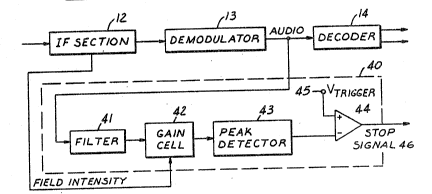
Figure 4 is a block diagram showing an improved
quality indicating circuit of the present invention.
Figure 5 is a plot showing a preferred gain
employed in the present invention as a unction of field
iI~tensity.
Figure 6 is a schematic diagram showing the
present invention in greater detail.
.,
2 ~ 2 ~
-- 5 --
Detailed DescriPtion of Preferred Embod _ents
Figure 1 shows a conventional FM receiver
architecture including an antenna lO, an RF section 11,
an IF section 12, a demodulator 13, a stereo decoder l~,
left and right audio amplifiers 15 and 17, and stereo
speakers 16 and 18. Electronic tuniny of the FM receiver
is accomplished by means of a scan tuner 20 which
provides a tuning voltage over a line 21 to RF section
ll. A local oscillator contained in RF section ll
provides a local oscillator signal for deriving an
intermediate fre~uency. The local oscillator signal is
also provided from RF section 11 to scan tuner 20 over a
line 22 for implementing electronic co~trol over the RF
tuning using a phase lock loop, for example.
Scan tuning of the FM receiver is implemented by
sweeping the tuning voltage provided over li~e 21 in
response to a start signal 23 provided to scan tuner 20.
Sweeping of the tun;ng voltage continues automatically
until an FM signal is received meeting the criteria for
identifying a signal of a predetermined quality. When
such a signal is received, a stop signal 24 is generated
by a stop circuit 25 and provided to scan tuner 20. An
intensity signal is provided from IF section 12 to stop
circuit 25 and an automatic frequency control (AFC)
sîgnal is provided from modulator 13 to stop circuit 25.
As taught in the prior art, stop circuit 25 generates a
stop signal in response to the intensity signal being
above a predetermined intensity and the AFC signal being
within a range of voltages defining a frequency window to
indicate that the station is accurately tuned in.
The present invention exploits the unique
characteristics of received FM signals of varying
si.gnal-to-noise ratios in order to improve and simplify
the identification of high quality received FM siynals.
3S Figure 2A shows the receiver noise spectrum in
,
: :. . :: - ~ :
: :............... - ,
~.
.
2al2~2
,
-- 6 --
an FM receiver when no received signal is being
detected. Spectrum 26 demonstrates that receiver noise
is nearly constant over a wide frequency range as would
be expected for the reception of no broadcasted signal.
Figure 2B shows a receiver noise spectrum 27
during reception of a weak signal. Spectrum 27 is
shifted toward lower ~requencies corresponding to a
modulated information signal including a stereo
difference channel. Noise voltage falls with increasing
frequency in the spectrum.
Figure 2C shows a receiver noise spectrum 28
during reception of a strong station. Spectrum 28 has
increased voltage at low fre~uencies, with voltages at
frequencies above about 150 KHz being substantially
reduced relative to the lower frequencies.
Figure 3 plots signal-to-noise ratio between the
information component and noise component versus
increasing ield intensity which results as the received
signal quality increases. A line 30 shows the peak
signal voltage for the information component and line 31
shows the peak signal voltage for the noise component.
Thus, as field intensity increases, the separation of
lines 30 and 31 increases. This separation corresponds
to increasing signal-to-noise ratio, such as 35dB, 50dB,
and 60dB.
A trigger level 32 is shown which is used to
identify a high guality received signal having a selected
signal-to-noise ratio. Using field intensity as a
measure of information component peak voltage, the noise
component is multiplied by the ield intensity to produce
an amplified noise signal 33 which indicates signal
quality relative to any desired signal-to-noise ratio as
determined by the point at which signal 33 crosses
trigger level 32. In other words, the noise component
line 31 is modified according to the information content
,
-, :
2 ~ 2
.
or field intensity measure to derive a modified or
amplified noise siynal 33 which is compared with trigger
level 32 in order to identify the predetermined signal
quality.
S Figure 4 shows a preferred embodiment of a stop
circuit 40 according to the present invention. A filter
41 receives the audio output signal rom demodulator 13,
Filter 41 blocks the information component and isolates a
noise component portion of the audio signal. The noise
component is output from filter 41 to a gain cell 42.
' The field intensity signal frQm lF section 1~ is also
; provided to gain cell 4Z. The output of gain cell 42 is
coupled to a peak detector 43 having its output connected
to the inverting input of a comparator circuit 44. The
noninvertin~ input of comparator 44 is connected to a
trigger voltage Vtrigyer,at a terminal 45. The output
of comparator 44 provides a stop signal 46 for
terminating a scan operation when an FM signal is
' received having a signal-to-noise ratio greater than a
: ' 20 predetermined ratiol
Gain cell 42 provides a gain amplified noise
signal. The gain of gain cell 42 is an inverse function
of the field intensity signal such that the gain
decreases in response to an increase in the intensity
signal. Thus, the peak signal voltage of the noise
component is maintained above the trigger level at low
field intensities, but is allowed to fall below the
trigger level at higher field intensities. The amplified
noise signal is converted to a peak value by pealc
detector 43. The peak value is compared in comparator 44
against trigger voltage Vtrigger such that the output
o comparator 44 swings to a high output value ~i.e.,
generates a stop signal) whe,n the peak value of the
amplified noise is below the trigger value. When applied
to the scan tuner such as that shown in Figure 1, the
.
$ ~ ~
- 8 -
stop signal 46 causes the tuner to stop the scan tuning
operation.
Figure 5 shows a preferred relationship between
the gain applied by gain cell 42 to the noise component
versus the field intensity measured by the IF section.
Gain function 50 includes a relatively high gain portion
51 and a relativel~ low gain portion 52 separated by a
predetermined intensity 53. Thus, the gain applied to
the noise signal is at a high level when the received
field intensity is below the predetermined intensity 53.
The point at which line 33 crosses trigger level
32 in Figure 3 is controlled by the predetermined
intensity 53. Thus, by changing the magnitude of
predetermined intensity 53, stop signal 46 can be
adjusted to identify a signal-to-noise ratio of any
predetermined decibel level.
In Figure 6, filter 41 and gain cell 42 are
shown in greater detail. Filter 41 includes a capacitor
55 connected to receive the audio signal. Capacitor 55
is coupled to ground through a resistor 56 an~ to a
piezoelectric resonator 58 through a resistor 57. The
output of piezoelPctric crystal 5R is a noise signal as
determined by the pass band characteristics of filter
41. In a preferred embodiment, filter 41 provides a
narrow passband of about 2 KHz in width having a lower
cutof frequency of about 200 KHz. However, the noise
signal can be derived from any frequencies provided that
substantially all components o~ the information signal
are filtered out. This could also be achieved by a high
pass ~ilter having a lower cutof frequency in the range
of about 150 KHz or higher (i.e., frequencies below about
150 KHz must be blocked).
The noise signal from filter 41 is coupled to
gain cell 42 which includes a transistor 60 connected to
receive the noise signal at its base. Gain cell 42 also
",:: : ~
. - . ",: :
:
- 9 -
includes components for biasing transistQr 60. A
resistor 62 is connected between the collector of
tr~nsistor 6.0 and a supply voltage at a terminal 61, and
a resistor 63 is connected in parallel with a capacitor
64 be~ween the base and the collector of transistor 60.
The emitter of transistor 60 is coupled to ground through
a resistor 65.
The field intensity signal ;s coupled through a
resistor 70 to the base of a transistor 71. The
collector of tra~sistor 71 is connecked to the base of
transistor 67. The emitter of transistor 71 is coupled
to a reference voltage source 72 through a current
~: limiting resistor 77.
Reference voltage source 72 includes a supply
voltage terminal 73, a pair of voltage dividing resistors
74 and 75 connected in series between terminal 73 and
ground, and a capacitor 76 connected between the junction :
: of resistors 74 and 75 and grouna. Reference voltage
. source 72 provides a reference voltage VR.. A capacitor
~0 78 is connected between VR and the base of transistor
71.
A capacitor 66 has one end connected to the
junction between the emitter of transistor 60 and
resistor 65 and has its other end connected to the
collector of a transistor 67. The emitter of transistor
67 is connected to ground and the base of transistor 67
is coupled to ground through a resistor 68.
The collector output of transistor 60 is
connected to one side of a capacitor 80. The other side
of capacitor 80 is coupled to ground through a resistor
al and provides the ampliied noise signal to peak
detector 43.
In operation, the noise signal isolated by
filter 41 is amplified by transistor 60 and is passed
through coupling capacitor 80 to provide the amplified
.
2~2&~ 2
-- 10 --
noise signal. The gain of transistor 60 is controlled by
its effective emitter resistance. This resistarlce is in
turn controlled by transistor 67. When transistor 67 is
biased into conduction, the emitter of transistor 60 is
effectively grounded to AC signals through capacitor 66.
The resulting gain of transistor 60 is at a relatively
high level due to the low effective emitter resistance of
transistor 60. When transistor 67 is biased to its
nonconducting state, the effective elmitter resistance
seen by transistor 60 increases to the resistance of
resistor 65, thereby lowering the gain applied to the
noise signal.
The conduction of transistor 67 is controlled by
transistor 71 which is in turn controlled by the field
intensity signal and the reference voltage VR. When
transistor 71 is biased to its nonconducting state, the
base of transistor 67 is grounded through resistor 68.
When transistor 71 is biased into conduction, base
current for transistor 67 is supplied by the collector of
~ransistor 71.
Transistor 71 is a PNP transistor. Therefore,
it is turned on when }ts emitter voltage is greater than
its base voltage by a threshold voltage which is
characteristic of the PNP transistor. This threshol
voltage is typically about .6 volts. Thus, transistor 71
is in conduction as long as the field intensity signal
provided through resistor 70 has a DC voltage less than
voltage reference VR minus .6 volts. To compensate for
that dif~erence, VR is set to be about .6 volts above
the desired trigger level.
By controlling reference voltage VR~ the point
at which the amplified noise signal crosses the trigger
level can be set at a desired signal-to--noise ratio. For
purposes of providing a stop circuit for a scan tuner,
the desired signal-to-noise ratio can be set at a fixed
.. .. ~ -
~ o~
level, such as about 30 dB. It is also possible to vary
reference voltage VR prior to a scan operation in order
~o scan for local or distant broadcast stations, for
example. Such variable reference Yoltages could be
provided under control of a microprocessor and a
digital-to-analog converter, for e~ample. Alternatively,
the present invention could be used to indicate the
presence of a signal having a predetermined
signal-to-noise ratio, or a plurality of circuits could
be employed to graphically display the received
signal-to-noise ratio.
While preferred embodiments of the invention
have been shown and descrihed herein, it will be
understood that such embodi~ents are provided by way of
e~ample only. Numerous variations, changes, and
substitutions will occur to those skilled in the art
without departing from the spirit of the invention.
Accordingly~ it is intended that the appended claims
cover all such variat;ons as fall within the spirit and
scope of the invention.
, . - ,
- . . ~ , .,
. - ;- -