Note: Descriptions are shown in the official language in which they were submitted.
20269 6 1
Fiber Optic Saqnac Interferometer with Diqital Phase
Ramp Resettinq for Measurement of Rate of Rotation
The present invention is related to co-pending
Application Serial No. 2,026,962 filed October 4, 1990.
The invention relates to a fiber optic Sagnac
interferometer for measurement of rate of rotation, in which two
light beams originating from a light source and generated by beam
splitting are irradiated into a fiber coil in opposite directions
and subsequently reunited, in which the interference pattern
produced is scanned by a detector device whose output signal
corresponds to the light intensity of the interference pattern,
in which with the aid of a phase modulator located in the fiber
coil the two light beams are modulated by a periodic rectangular
signal combined from a plurality of variable signal components
and having the fundamental frequency fO = 1/2to, to corresponding
to the transit time of each of the light beams through the fiber
coil, and in conjunction with periodic change in the modulation
deviation a first signal component effecting between two
operating modes in time with the frequency fO a reciprocal
alternating phase shift of the two counter-rotating light beams,
and, furthermore, a second signal component being a stair-step
ramp signal whose risers each have a duration, corresponding to
the transit time to or integral multiples of to~ and amplitude
increments which compensate nonreciprocal incremental phase
shifts of the two light beams, in which the amplified
photodetector output signal is fed to a first synchronous
demodulator clocked with the frequency fO, in which the
demodulated and amplified output signal is fed to an analog-to-
digital converter and after digitization integrated in a digital
integrator and via a digital-to-analog converter and a driver
amplifier applies nonreciprocal phase shifts of the light beams
to the phase modulator via the phase compensating the second
signal component, in which a scale factor correction circuit is
provided which demodulates the amplified photodetector output
signal in time with the mode reversal and transmits an analog
scale factor correction signal to the digital-to-analog converter
, ~
B ~s
202696 1
a
via an integrating amplifier, and in which a processor clocked
by the quartz oscillator supplies the control and synchronization
signals for the first synchronous demodulator, the analog-to-
digital converter and the digital integrator.
The known prior art is discussed below. Since
reference is made in this discussion to the accompanying
B
2 0 2 69 6 1
_ drawings, these are first briefly introduced, as follows:
Fig. 1 shows the already explained change in the ramp
gradient of the resetting signal, which change is
dependent upon the change in modulation
deviation, that is to say the operating mode;
Fig. 2 shows the likewise already explained production
of the lock-in effect in the case of low rates of
rotation;
Fig. 3 shows a first illustrative embodiment of an
interferometer arrangement according to the
invention for measurement of rate of rotation;
Fig. 4 shows a modified embodiment of the arrangement
according to Fig. 3;
Figs. 5 to 13 show signal shapes to explain the mode of
operation of the circuits according to Figs. 3
and 4; and
Fig. 14 shows an arrangement,
corresponding to the prior art, of a fiber optic
interferometer with digital processing of the
rate-of-rotation signals and generation of the
modulation deviation signals and of the ramp
resetting signal.
In order to measure nonreciprocal phase shifts in a
fiber optic Sagnac interferometer, also known as a ring
interferometer, it is known from the printed publicaticn DE-Al-
3,144,162 to readjust the nonreciprocal phase shifts, e.g. on the
basis of rates of rotation, by applying to the phase modulator
located in the region of an input of the fiber coil a phase
deviation which has a specific amplitude and can be reversed with
the frequency fO = 1/2 to, on the one hand, and a saw-toothed
voltage which likewise shifts the phase deviation on the other
hand, to designating the transit time of each of the light beams
through the fiber coil. The gradient of the compensating or
resetting saw-toothed voltage (phase ramp) corresponds to the
rate of rotation, and is thus proportional to ~o/to, ~0
designating the nonreciprocal phase shift, for example caused by
a rotational movement. In practice however it is scarcely pos-
sible to make use of the so-called phase ramp resetting method
described in the said DE printed publication, because the iner-
tial measurements of rates of rotation require accuracies, in
A
_ 3 - 2~26961
-~ _ particular with respect to the reversible phase devia-
tions, the amplitude or gradient of the resetting signal
and the proportionality or scale factor which cannot be
guaranteed in analog circuit engineering.
US-A-4,705,3~9 (= EP-A1-0,168,292) has disclosed a
remar~able further development of the ramp resetting
method for fiber optic ring interferometers described in
principle in the said DE printed publication, which
operates entirely digitally for signal evaluation and
conditioning, so that, particularly with respect to the
accuracy of the reversible phase deviations and of the
ramp resetting signal the required signal precision can
be obtained by a unique allocation of an automatic
measuring range reversal and a correction of the scale
factors. The functional principle of the digital phase
ramp resetting method for fiber optic rate-of-rotation
sensors according to the prior art is first explained
with reference to Fig. 14, which corresponds - in a
simplified representation - to the prior art according to
Fig. 14 of the said printed publication US-A-4,705,399
(cf. also H.C. Lefèvre et al. in Integrated Optics: "A
practical solution for the Fiber-Optic Gyroscope', SPIE
Vol. 719, Fiber Optic Gyros, 1986), reference being made
with respect to the details to the said literature:
The schematic representation of Fig. 14 of a Sagnac
interferometer corresponding to the said prior art and
having a closed fiber loop shows a light source L, for
example a laser, whose parallel light beams are split
into two light beams via a beam splitter ST1, and are
irradiated into an interferometer fiber coil FS in the
opposite direction. The fiber coil FS will preferably
consist of an optical monomode fiber. The beam splitter
ST1 acts simultaneously as a mixer for recombining the
two light beams after traversal of the fiber coil FS. The
interference signal of the two superimposed light beams
passes via the second beam splitter ST2 and the output
branch OuT ~hereof to a photodetector PD, which scans the
intensity of the interference pattern. Using ^~0 to
designate the phase difference between the two light
A
~ 4 - 2026961
_ beams that propagate in opposite directions in the closed
fiber coil FS, it holds that, so long as there are no
- nonreciprocal distur~ances, ~0 = 0. Reference should be
made to the literature cited concerning the mathematical
relation between the phase difference ~0 and the rate of
rotation or rotational speed, the optical power density
at the input of the photodetector PD, and the measuring
sensitivity. It is also described there how the sensi-
tivity of the interferometer can be increased by intro-
ducing a constant, nonreciprocal bias to be applied tothe two counterrotating light beams in the fiber coil FS,
to be precise in such a way that the two counterrotating
light beams (light waves) are periodically shifted, by
means of a phase modulator PM, to the operating point of
highest sensitivity of the interferometer by angles of
(2n + 1)~/2, n being a whole number. For this purpose,
the phase modulator PM is thus first excited with a
signal ~1(t), which effects a periodic phase shift of for
example + ~/2, 3/2~, ..., and whose period is 2to, to
designating the transit time of a light wave in the fiber
coil FS.
In the case of the circuit according to Fig. 14,
nonreciprocal phase shifts from negati~e feedback to the
phase modulator PM are compensated, as described in the
said US Patent, by a so-called phase ramp signal, whose
gradient is proportional to ~/t~, i.e. to ~, that is to
the nonreciprocal phase shift. In the case of the circuit
according to Fig. 14, the resetting phase ramp signal is
a saw tooth or staircase signal, in which the amplitude
of a saw-tooth or the height of a riser is equal to ~,
while the duration of a saw-tooth or of a riser corres-
ponds to the transit time t~ or to an odd-numbered
multiple of to-
By comparison with an analog solution, this digital
phase ramp principle described in the literature, inparticular the said US-A-4,705,3g9, has the decisive
advantage that the scale factors of the phase modulation
control signal and the phase ramp resetting signal are
corrected, at least in principle, and that a precise
- ~26961
definition of the saw-tooth amplitudes of the resetting
signal is guaranteed.
The function of the circuit according to Fig. 14,
namely to generate a reciprocal phase shift alternating
in time with the frequency f~ and optLmizing the operating
point, and the stair-step ramp resetting signal including
a scale factor regulation, is explained briefly below:
- The output signal VD of the photodetector PD is
raised ~ia an impedance convertor and amplifier Ab, whose
output signal vD' feeds a synchronous demodulator SYNCD,
which is synchronized to the scanning frequency fO= 1/2t~.
The demodulated output signal passes as the signal VA ~ia
an amplifier A, which is combined, as a rule, with a
filter, to an analog-to-digital convertor AD, whose
digital output signal is proportional to the rate o~
rotation and contains an item of,sign information with
respect to the direction of rotation. The signal VAD then
passes to a circuit GSC, which essentially contains a
digital integrator and supplies a combined phase control
signal vsc, as combined signal consisting of the digital
phase ramp resetting signal and the digital phase modula-
tion signal. The combined digital signal VSC is subse-
quently converted in a digital-to-analog convertor DA
into an analog control voltage VC, and transmitted via a
driver amplifier AP as control voltage to the phase
modulator PM.
The circuit GSC for generating the signal VSC
comprises a first memory M1 for intermediate storage of
the digital signal VAD, whose intermediately stored
output signals SMI pass to a first input el of an adder
ADD, which is connected in cascade to a second memory M~.
The output signals vsc intermediately stored in the
second memory ~2 are fed back to a second input e2 of the
adder ADD and added to the digital value of the rate-of-
rotation signal. The output signal SADD of the adder ADDthus corresponds to the angle of rotation.
The circuit described so far for generating the
phase modulation signal and the phase ramp resetting
signal is synchronized and controlled by a central
6 20~96:~
processor CPU via a bidirectional bus BC, which is
connected to a quartz-stabilized 05cillator OSC, which
supplies the frequency f~.
Aside from the number of bits per word, which
number is referred to a specific angle of rotation, e.g.
four seconds of arc, which bits correspond to the capa-
city of the adder ADD, said adder supplies an overflow
signal at an output SL via the bus BC to the central
processor CPU. DepPn~ing upon the overflow signals of the
adder, and in agreement with the clocX signal of the
oscillator OSC, the central processor CPU generates the
various control and synchronization signals, it being the
case that, in order to enable a scale factor correction,
a switchover is made, depending upon the overflow of the
adder ADD, of the modulation deviation between a "mode A"
and a "mode B", in such a way that a modulation deviation
of, for exzmple, +~/2 holds for mode A, and a modulation
deviation of t3/2~ holds for mode B. As is described in
the literature cited, the detected amplitude differences
between the operating states with different modulation
deviations are a measure of the scale factor error at the
instances of phase ramp signal overflow. In order to
correct this scale factor error, the ~nown circuit
according to Fig. 14 is equipped with a demodulator SFC,
which detects the amplitude differences of the fO modula-
tion signal in mode A (phase deviation e.g. +~/2) and
mode B (phase deviation e.g. +3/2~), and transmits this
demodulated signal as an analog correction signal SIA via
an integrating amplifier IA to a correcting analog input
e~ of the digital-to-analog convertor DA.
This functional principle of the digital phase rAmp
resetting method for fiber optic rate-of-rotation
sensors, which has been described briefly with reference
to Fig. 14 and in which the gradient of the phase ramp is
a measure of the reset rate of rotation, and in which in
the return phase there is a reversal of the modulation
de~iation in a ratio 1:3 in order to obtain a correction
signal for the scale factor, leads in the practical
operation of such parasitic rate-of-rotation measuring
- - 7 - ~ ~269~ 1
devices to substantial difficultles for the following
reasons: -
The reversal from "mode A~ to "mode B" is directlydependent upon the ramp ~alue of the resetting saw-
toothed signal and thus upon the angle of rotation of thegyroscope. In this regard, a ramp traversal can corres-
pond to an angular inc~ nL of, for example, approxi-
mately four seconds of arc. However, via the trebling of
the amplitude of the modulation signal and via parasitics
of the latter in the sensitive signal path of the photo-
detector signal VD, the modulation deviation reversal
- effects a reversal of the gyroscope biasj These undesired
parasitic effects are indicated in the circuit according
to Fig. 14 by dashed lines and the coupling factor R.
Since this reversal of the modulation deviation signal
is, however, dependent upon the angle of rotation, it
leads to a dead band (lock-in) of the gyroscope. As is
explained below, it is also possible to show that this
effect leads to a scale factor nonlin~rity outside the
lock-in zone.
As is shown in Fig. 13 of the printed publication
US-A-4,705,3~9, given the occurrence of a scale factor
error there is a different mean intensity I of the
photodetector signal VD in the case of modulation devia-
tions of mode A or in the case of the modulation devia-
tions of mode B. This intensity difference is integrated
in the integrating amplifier IA, and supplies the analog
correction signal at the input eH f the digital-to-analog
convertor DA. The fre~uency of change in intensity is
equal to the frequency of change from mode A to mode B,
and thus equal to the ramp signal return frequency, since
the reversal, e.g. from mode A to mode B, is produced by
ramp overflow, i.e. the signal SL of the adder ADD. This
frequency of change is proportional to the rate of
rotation, i.e. in accordance with the example explained
in the said US Patent, a return of 2~ corresponds to an
angular increment of 5 seconds of arc; at a 1 Hz return
frequency this corresponds to a rate of rotation of 5/h.
In the case of low rates of rotation, this frequency
8- 2~2691~1
of change can become arbitrarily low, and for this reason
the integrating ampli~ier La only seldom contains the
information on intensity difference. In the then arbit-
rarily long inter~als in which the mode does not change,
the integrating amplifier IA does not have this informa-
tion, and every small electrical zero error at its input
causes its output quantity, that is to say the scale
factor correction signal SIA, to drift. For this reason,
at low rates of rotation the scale factor is susceptible
to drifting of the integrating amplifier IA. It is true
- that the percentage error in the rate of rotation caused
by scale factor drifting, expressed in absolute values of
rates of rotation, is small for low rates of rotation.
~owever, a sudden sharp rise in the rate of rotation,
lS above all, does become probl~atic, since then the scale
factor is still "wrong~, and thus high absolute errors in
the rate of rotation also occur, at least until the scale
factor control circuit is once again in the steady-state
condition.
It would now seem to be advisable to seek to c~ove,
or at least reduce, the electromagnetic parasitics
(disturbances with a coupling factor ~; see Fig. 14) by
means of electro-magnetic compatibility measures (EMC
measures), that is to say in particular by shields
(indicated in Fig. 14 by shielding the connecting line
from the driver amplifier AP to the phase modulator PM)
and installing filters in the signal and voltage feed
lines. However, with the known interferometer design
according to Fig. 14 there are special E~C problems: the
signal VS~ or VC, VC' contains the modulation frequency
fO = 1/2to, which is generatad in the oscillator OSC or
via the processor CPU. However, the photodetector signal
VD contains the information on rate of rotation with the
same frequency and phase angle. This signal is detected
in the synchronous demodulator SYNCD. The circuit g~oups
which generate the modulation quantity of frequency fO,
and the circuit part-q which conduct the signal of the
same frequency, which is sensitive to the rate of rota-
tion, are closely connected in space and have, by and
- 9 - 2026961
large, to be fed from a common power supply device. This
~ clearly presents the danger that electromagnetic energy
of frequency f~ will parasitically enter the sensitive
signal path (signal VD). Stop filters for fa in the signal
lines are not possible, since the desired signal informa-
tion is present at just this frequency. Undesired para-
sitics can thus, for example, be reduced to a certain
extent only by shielding the amplifier ~ and the
synchronous demodulator SYNCD against the remainder of
the circuit, and by filtering their power supply.
A numerical example for the parasitic sensitivity
will immediately clarify the particula~ problems for a
person skilled in the art. This spectral component with
frequency f~ in the signal VC or VC' is generally located
in the range of a few V. By contrast, in the rate-of-
rotation signal VD voltages in the range of a few nV
correspond - depending upon optical power, detector
sensitivity and gyroscopes scale factor - to a rate of
rotation of 1/h. In the case of such large amplitude
differences, an undesired parasitic path will be unavoid-
able despite all possible EMC measures, as is symbolized
in Fig. ~4 by the coupling factor R between the signals
VC, VC' and VD; naturally, with different parasitic
amplitudes, and thus with different errors, equivalent to
rates of rotation, in the signal VD, to be precise
depending upon the operating state mode A or ~ since, as
assumed, the latter has a modulation amplitude three
times higher than the former, and thus has a stronger
parasitic effect. These different parasitic amplitudes
lead, with reference to rates of rotation, to different
gyroscope zero point errors which are designated as
biases Ba or B~, depending upon the instantaneous modula-
tion state mode A or mode B.
~hus, the ramp gradient of the resetting signal is
regulated via the closed control circuit in a m~nner
proportional to the sum of the true input rate of rota-
tion D~ and the respective bias B~ or B~, depending upon
whether modulation mode A or B is present.
In Fig. 1 of the attached drawings, an example is
- 10 - 202fig~1
represented in which D. + B~ > 0, D. + ~ > 0 and Ba '
holds, that is to say different biases Ba or ~ are
present. If it is assumed that Da = const., different ramp
gradients are produced dep~n~i ng upon whether mode A or
mode B is present at the instant, since the ramp gradient
is regulated in a m~nnPr proportional to D~ + Ba or in a
m~nne~ proportional to De + B~.
In the example represented in Fig. 1~ the gradient
during mode B is flatter than in the mode A, since ~ < Ba
is assumed. Thus, the dwell time tb in mode B is larger by
comparison with the dwell time t. in mode A than would be
the case for biases independent of modè (Ba = ~). How-
evèr, since not only B~, ~ but also the input rate of
rotation ~, influence~ the ramp gradient in both modes,
the pulse-duty factor of the modes (Ta/T~) also depend~
upon D.. The scale factor nonl inP~rity addre~sed abo~e
results from this.
On the other hand, the abov ~_ntioned lock-in
effect occurs in a rate-of-rotation range in which the
sum (De I B~) or (D. + E~) has a different sign for the two
modes, i.e. when it holds, for example, that (D. + B~) ~ 0
or (D. + ~) < 0. This case, entirely realistic for low
rates of rotation, is represented in Fig. 2:
The ramp of the resetting signal (illustrated without
modulation for the sake of clarity of representation)
starts, e.g. in mode A with a positive gradient, since (D~
+ Ba) > 0 applies, as assumed. When the ramp reaches the
(upper) overflow range (overflow signal SL in Fig. 14),
a switch is made to mode B. However, the control then
triggers a negative ramp gradient, since it now holds
that (Dg + ~) ~ 0, i.e. the ramp gradient changes its
sign and thus leaves the overflow region, and mode A once
again holds. However, a positive ramp gradient once again
belongs to this mode A, until reversal to mode B taXes
place once again, etc. Thus, the control is held
captive , i.e. the interferometer arrangement is in the
lock-in state. How quickly the 'zig-zag-ramp represented
in Fig. 2 between the modes A and B changes at the over-
flow limit is detPrm;n~ by the rapidity of the control;
202696 1
this is in general very high. The lock-in state holds for
an input rate-of-rotation range in which the specified
inequalities are fulfilled, i.e. the loc~-in range thus
has a width of I Ba ~ ~ I -
In the description given so far, the particular ramp
value is taken to be the instantaneous value of the
(unmodulated) ramp ~(t). This ramp value is proportional
to the angle of rotation and corresponds to the signal
SADD. The ramp gradient d~/dt corresponds to the time
derivative of the angle of rotation, that is to say the
rate of rotation. To put the matter plainly, the problem
of the known ramp resetting method is that the ramp
value, i.e. the value of the angle of rotation, is the
criterion for whether operating mode A or B and thus the
different biases B~ or ~ are present and because of B~ ~
~ influence the ramp gradient itself. The scale factor
error information is present, as represented, in the form
of a signal of change in intensity, whose frequency is
proportional to the rate of rotation and can vary between
0 and approximately 100 kHz, when the theoretical pulse-
duty factor of the modulation deviations between mode A
and mode B is 1: 3. The apparent advantage that the
information-carrying changes in intensity occur more
often at high rates of rotation and, as a consequence, a
better scale factor error information is present at high
rates of rotation, is opposed, however, by the fact that
the associated signal processing device has to process a
comparatively high frequency range. However, as
represented, in the region of the zero rate of rotation
the known ramp resetting method leads, on the other hand,
to the absence of the scale factor error information and
thus to drift problems.
It is therefore the object of the invention to
avoid the dead band of a fiber optic rate-of-rotation
sensor in the case of low rates of rotation, i.e. the
lock-in effect represented, and to obtain signals that
are easy to process for the purpose of controlling the
scale factor.
A
- ~ -11a- 2026961
According to one aspect of the invention there is provided a fiber optic
Sagnac interferometer for measurement of rate of rotation, in which: (a) two light
beams originating from a light source and generated by beam splitting are
irradiated into a fiber coil in opposite directions and subsequently reunited, (b) the
interference pattern produced is applied to a detector device whose output signal
corresponds to the light intensity of the interference pattern, (c) with the aid of a
phase modulator located in the fiber coil the two light beams are modulated by aperiodic rectangular signal combined from a plural ity of variable signal components
and having the fundamental frequency fO = 1/2to, where to = the transit time of
lo each of the light beams through the fiber coil, (i) in conjunction with periodic
change in the modulation deviation a first signal component effecting between two
operating modes (A, B) in time with the frequency fO a reciprocal alternating phase
shift (¢IM) of the two counter-rotating light beams, and (ii) a second signal
component being a stair-step ramp signal whose risers each have a duration,
corresponding to the transit time to or integral multiples of to~ and amplitude
increments which compensate nonreciprocal incremental phase shifts of the two
light beams, (d) the amplified photodetector output signal is fed to a first
synchronous demodulator clocked with the frequency fO, (e) the demodulated and
amplified output signal is fed to an analog-to-digital converter and after digitization
integrated in a digital integrator and is applied to the phase modulator via a digital-
to-analog converter and a driver amplifier, in order to compensate nonreciprocalphase shifts of the light beams by means of the second signal component, (f) a
scale factor correction circuit is provided which demodulates the amplified
photodetector output signal in time with the mode reversal and transmits an analog
scale factor correction signal to the digital-to-analog converter via an integrating
amplifier, and in which (g) a processor supplies the control and synchronizationsignals for the first synchronous demodulator, the analog-to-digital converter and
the digital integrator, wherein: between the digital integrator and the digital-to-
analog converter there is arranged a digital adder to which at a second input the
modulation deviation signal that can be reversed with the predetermined timing
between the two operating modes (A or B) is applied from a first pulse generatorthat is clocked with the frequency fO and transits to the second input of the digital
A
.
12 202696 1
adder a signal corresponding to the phase deviation +~/4 for the
first operating mode (A) and a signal corresponding to the phase
deviation +3~/4 for the second operating mode (B).
It was recognized, as already explained with reference
to Figs. 1 and 2, that the automatic change in modulation
deviation as a function of the angle of rotation is the main
cause in the event of ramp overflow of the lock-in effect of the
known method, of the scale factor nonlinearity and of the wide
frequency range of the scale factor error information, which
range is a function of the rate of rotation. Accordingly, the
invention is directed towards the goal of developing a modulation
method to set up a ramp resetting method which comprises, on the
one hand, the reversal of the modulation deviation from mode A
to mode B with order to obtain the scale factor error information
while, on the other hand, stipulating this reversal with a
specific, e.g. fixed timing and no longer as a function of the
angle of rotation.
Starting from the known ramp resetting method, in the
case of a fiber optical Sagnac interferometer for measurement of
rate of rotation according to the generic concept explained at
the beginning of this disclosure, the invention consists in that
between the digital integrator and the digital-to-analog
converter there is arranged a (second) digital adder to which at
a second input the modulation deviation signal that can be
reversed with the predetermined timing between the two operating
modes is applied from a first pulse generator that is clocked
with the frequency fO and transmits to the second input of the
(second) digital adder a signal corresponding to the phase
deviation +~/4 for the first operating mode A and a signal
corresponding to the phase deviation +3/4~ for the second
operating mode B.
2026961
.,
13
The invention and advantageous details are explained
in more detail below in illustrative embodiments.
The arrangement groups, circuit groups and signals
already known from the explanation of Fig. 14 are referenced in
Figs. 3 and 4 with the same symbols. The description of the
functional relationships that are already known to the reader
will not be repeated. The first step is to describe the mode of
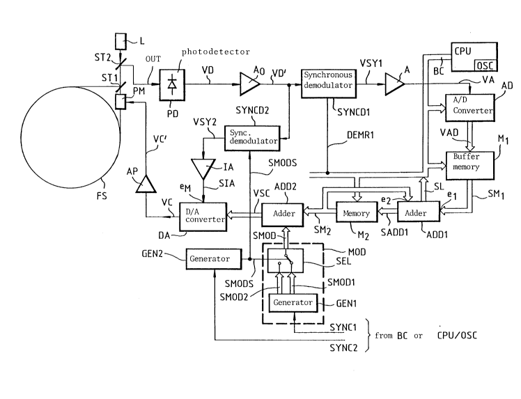
operation of the arrangement according to Fig. 3:
The photodetector PD observes the light intensity I of
the interferometer output signal, and supplies a corresponding
signal VD, which is amplified in the amplifier Ao~ to the signal
VD'. The light intensity signal I contains information on
1) the system deviation of the rate of rotation, which
leads to a change in intensity ~Io with the frequency fO
and which is detected in the (first) synchronized
demodulator SYNCD1, with the aid of a signal DEMR1,
which is supplied by the processor CPU and is of the
same frequency, to the output signal VSY1. The
frequency fO is, in turn, the interferometer operating
frequency, which is given by fo=1/2 to it being
- 14 - ~02~961
the case that to = n x l/c where n = refractive index
of the light guide material of the fiber coil FS,
l = optical path length in the fiber coil FS and
c = ~elocity of light in the vacuum;
2) the system deviation of the scale factor, i.e. a
de~iation in the deviation of the phase modulation
of the electrooptic phase modulator PM in the inter-
ferometer, which leads to a change in intensity ~
(cf. Fig. 12) between the modulation mode~ A and B
with the frequency of a modulation de~iation
reversal signal S~ODS, which is explained in more
detail further below and is generated in a pulse
generator OE N2 designated as second generator, and
can be synchronized with the gyroscope operating
frequency fO via a signal SYNC2 supplied by the
processor CPU. This difference in intensity ~I1 is
detected in a (second) synchronous demodulator
SYNCD2 with the aid of the signal SMODS and the
result is a signal VSY2 which is a measure of the
scale factor error and is, as already Xnown from the
circuit according to Fig. 14, applied via the
integrating amplifier IA to an analog setting input
e~ of the digital-to-analog converter DA.
For the sake of improved clarity, first the rate-
2S of-rotation control circuit will be explained below,
followed by the scale factor control circuit.
Re 1): Rate-of-rotation control circuit
The signal VSY1 which corresponds to a system
de~iation of the rate-of-rotation control circuit is
amplified in the amplifier A and supplies the signal VA.
The amplifier A simultaneously comprises a filter, which
determines the technical control characteristics of the
entire control circuit and is ~im~ncioned according to
known design procedures in control technology; to this
extent, referencs i~ made to the printed publication
US-A-4,705,39~, which has already been addressed more
than once. In practical terms, the output signal V~ will
ha~e a component of the time integral of the input signal
VSY1. The signal VA is digitized in the analog-to-digital
2026961
- 15 -
con~erter AD, and the digital signal vAD produced is-
stored in the memory ~1, these processes being controlled
by the processor CPU via the bus BC. As is already ~nown,
the output signal SMl is applied to the input e1 of the
adder, which is designated here, for the sa~e of better
differentiation of a further adder, as first adder ADD1.
The output signal SADD1 of the first adder ADD1 is fed to
the memory M2, whose output signal S~2 i5 fed to the
further input e2 of the first adder ADD1, entirely in
con~ormity with the known circuit according to Fig. 14.
The first adder ADD1 represents, in con~unction with the
memory M2 and the allocated control via the bus BC, a
ramp signal generator, which generates a ramp signal or
staircase signal SM2, whose riser height correspond to
the value SM1, and whose step width corresponds to the
optical transit time t~.
By limiting the word length of the digital
processing device consisting of the first adder ADD1 and
the second memory M2, a ramp overflow of the signal SM2
is achie~ed when a specific output value of the first
adder ADD1 is exceeded, which is represented
schematically in Fig. 5. In this regard, it is possible
to exploit the overflow characteristics of digital binary
number codes ad~antageously.
This signal, designated as second signal
component SM~, is fed - other than in the known circuit
according to Fig. 14 - to the optical phase modulator PM
via electronic modules still to be described, and effects
a phase shift ~Rt which is limited by the abovementioned
overflow t~ a phase range of essentiaily 2~ (cf. Fig. 5).
According to the invention, an essentially
rectangular modulation siqnal SNOD is added in a second
adder ADD2 to the signal SM2, thus producing the combined
modulation signal VSC. The modulation signal SMOD is
generated in a modulation signal generator NOD and has
the gyroscope frequency f~. The modulation signal
generator MOD is synchronized by the processor CPU or the
oscillator OSC via a signal SYNCl. The amplitude of the
signal SMOD can be varied by the factor 3 in a way to be
,- 16 - 2026 961
explained in yet more detail further below via a signal
, . . .
S~ODS. (cf. Fig. 6), which is ta~en from the already
- mentioned second pulse generator GEN2. The signal
component SMOD (cf. Fig. 7) is added in the second adder
ADD2 to the signal SM2, and fed to the optical phase
modulator PM via the driver amplifier AP after being
converted to the analog in the digital-to-analog
converter DA. This signal component SMOD effects a phase
shift ~ there, which is essentially +~/4 or +3/4~ (cf.
Fig. 7). The amplitude of the modulation ~ is thus
controlled by the signal SMODS. As already explained
above, the state during which the amplitude is +~/4 is
termed "mode A", while the "mode B" is set in the case of
the larger deviation in modulation amplitude of +3/4~.
As represented in Fig. 3, the modulation
amplitude reversal can take place, for example, such
that two signals SMOD1 corresponding to the explained
mode A and SMOD2 corresponding to the mode B are
generated in a generator GEN1 with the explained
amplitudes, and applied alternately as signal SMOD to the
second input of the second adder ADD2 via a changeover
switch SEL controlled by the signal SMODS.
The digital processing word width of the second
adder ADD2 is designed such that the output signal VSC
always corresponds to the sum of the input signals SM2 and
S~OD, without an overflow of the result occuring. The
combined signal VSC (cf. Fig. 8) is fed in the manner
already explained to the digital-to-analog converter DA
and converted into the voltage signal VC and amplified
to form the signal VC', whose value is essentially
proportional to the numerical value of the signal VSC.
The voltage VC' effects in the optical phase modulator PM
a phase shift ~c (see, once again, Fig. 8).
Thus, the circuit modified according to the
invention in conformity with Fig. 3 is based on the
following principle:
The unmodulated digital ramp value is limited by
truncation above the bit of significance ~ to the phase
angle range 2~ or + ~. Added to this limited ramp in the
`. 2026961
- 17 -
second adder ADD2 is a rectangular signal, which is
generated in the first pulse generator GENl, SEL or MOD
and has the modulation fre~uency Fa~ but which is
reversible in amplitude in accordance with a phase angle
value of ~/4 (mode A) and +3/4~ (mode B). This reversal
is controlled by the second pulse generator GEN2, wh~se
frequency and pulse-duty factor is freely selectable. The
re~ersal values can be per~n~ntly predet~rmined by the
processor CPU, or controlled as a function of the rate of
rotation, it being sensible to synchronize with the
modulation frequency fO.
Via the interferometer, the modulated ramp signal
represented in Fig. 8, which is fed to the phase
modulator PM, produces at the output of said interfero-
meter an intensity signal I(t) which essentially
satisfies the following relationship: -
I(t) - cos (~(t)+~o(t))
where a~ (t) = ~c(t) - ~c(t-to) is valid; ~c(t) is the
phase shift at the phase modulator PM and ~o(t) is the
Sagnac phase shift, which is proportional to the rate of
rotation and is given by
d 2~ ; ~ D . n
Here, 1 designates the length and D designates the mean
diameter of the optical path in the fiber coil, FS, ~ the
wavelength of the light employed, c the velocity of light
in the vacuum and n the rate of rotation.
The signal ~(t) is represented in Fig. 9. Fig.
10 reproduces the resultant variation in intensity as a
function of ~(t) and ~o(t). As may be seen from these
two figures, the phase shift ~o(t) that is proportional
to the rate of rotation leads to t~e fact that the
intensity I rise~ in the time inter~ai-q ~ and ~IV~ and
falls in the time intervals "II", ~ or ~V". The
resultant variation in intensity with time I(t) is
represented in Fig. 12.
The difference in intensity AIo is, as mentioned
above, detected with the aid of the first synchronous
- 18 - 2026961
demodulator SYNCD1 and serves to control the ramp gra-
dient of the signal ~R (cf. Fig. 5), the effect of ~0
being compensated by the mean value of the phase shift
~, which has the same modulus but a different sign. It
then holds for the intensity I(t) that: -
I(t) - cos (~(t)) = const.
It follows from this that the ramp gradient of ~R is a
measure of the rate of rotation.
Instead of the rate of rotation ~Rr it can be
ad~antageous to read out the angle of rotation as the
integral thereof. This can be done, for example, by
counting the abovementioned overflows of the ramp signal
SN2 at the output of the second memory M2 or of the
output signal SADDl of the first adder ADD1. An overflow
and, resulting from this, a return in the phase angle ~R
by 2~ corresponds in this process to an angular increment
of-
D
When an interferometer with a fiber coil diameterD = 6 cm is used, the abovementioned angular increment Q
is approximately 4 angular se~onds. This overflow
information can, for example, be given by the first adder
ADD1 via its overflow output signal SL and the bus BC to
the processor CPU, which counts the angular increments
(sums them up).
Scale factor control circuit
As explai~ed above, the output signal VSY2 of the second
synchronous demodulator SYNCD2 is a measure of the scale
factor error. This error signal is applied to the
integrating amplifier IA, which represents a filter which
is ~imen-~ioned from a standpoint of control engineering
and determines the control-engineering properties of the
scale factor control. The output signal SIA contains at
least one component which corresponds to the time
integral of the input signal VSY2. As also in the case of
the known circuit according to Fig. 14, the signal SIA is
'A
19- 2~26961
fed to the input eM f the digital-to-analog converter DA.
The digital-to-analog converter DA may be de~ignated as
multiplying digital-to-analog converter, i.e. its output
quantity VC i5 essentially proportional to the product of
the two signals VSC (digital) and SIA (analog). Thus,
with the aid of the information on differences in inten-
sity ~I1 (Fig. 12) the voltage de~iation of the signal VC
is controlled in such a way that the modulation phase
de~iation at the optical phase modulator PM is exactly
+~/4(mode A) or +3/4~ (mode B). It is thus ensured at the
same time that the return of the phase ~ occasioned by
the overflow (cf. Fig. 5) corresponds exactly to 2~.
Fig. 11 represents how, given the presence of
scale factor errors - here, for example, of the type such
that the optical phase shift i~ present to a lesser
extent than desired - the operating points I, II, III,
IV or V, which determi ne the variation in intensity, are
shifted to the operating points I', II', III', IV', V',
and thus how the abo~ementioned change in intensity ~Il
(Fig. 12) is produced. By feeding the appropriate
correction signal SIA to the input eM of the digital-to-
analog converter DA, the output amplitude of the signal
VC and thu~ the optical phase shift are increased such
that the desired operating points I, II, III, IV, V are
reached again and the change in intensity ~Il vanishes.
For the sake of completeness, Fig. 13 further
shows the qynchronization signal DEMRl to be fed to the
first qynchronous demodulator SYNDl ~ia the bus BC.
The (partial) circuit represented in Fig. 4
corresponds entirely in its mode of functioning to that
according to Fig. 3. The only difference is that the
second synchronous demodulator which is formed here - in
a manner analogous to Fig. 14 of the printed publication
US-A-4,705,3g9 - by two difference amplifiers A14 and
A23, respecti~ely, to whose positive or negative inputs
the signals VSl, VS2 or VS4, VS3 of four sample-and-hold
circuits are applied in a manner not represented in more
detail. However, there iq a difference from the known
circuit in that the changeover switch ~2 on the output
~ - 20 - ~ ~ %69~
,
side, via which the signal of change in intensity is,
finally, applied to the integrating amplifier IA, is
controlled by the freely selectable, but fixed output
signal S~ODS of the second pulse generator GEN2, that is
to say in time with the p~rm~nently predetermined mode
deviation reversal or modulation de~iation reversal.
It is true that in the circuit m~dified according
to the invention, for example in conformity with Fig. 3
or 4, an interference of the different modulation devia-
tion does continue to effect a change in bias. However,the latter is no longer a function of the rate of rota-
- tion but rather its value is constant a~d corresponds to
the mean value, weighted in terms of the pulse-duty
factor, of the bias values of the two modulation devia-
tions. Since the frequency and the pulse-duty factor
error with which the change in modulation deviation is
controlled and with which the scale factor error informa-
tion occurs, are freely selectable within wide limits and
are, above all, known, the scale factor control can be
optimized to a fixed frequency.
By contrast with the known implementations for a
fiber optic inertial rate-of-rotation sensor with digital
phase ramp resetting, the invention offers the decisive
ad~antage that the described lock-in effect and the scale
factor nonlinearity bound up therewith are avoided, and
that signals that are more advantageous to process are
present for scale factor control.
The elaborate EMC measures previously held to be
necessary for gyroscope electronics can be avoided, at
least part-ly.
The extra expenditure on cir~uitry required in
the digital part of the control electronics is relatively
low, and is not of importanc~ in the use of modern
inteqrated circuits.
Since the range of modulation of the phase
modulator P~ is slightly increased, this also requires a
somewhat higher capacity for modulation in the analog
driver components and an increase in the resolution of
the digital-to-analog converter DA by 1 bit. However, in
~ - 21 - 2026961
the light of the considerable practical advantages of the
implementation according to the invention this slight
extra expenditure is negligible.
If, and to the extent that, the statements above
and the patent claims given below start from the
n~me~tal or interferometer operating frequency fa =
1/2to, it may be expressly mentioned that the device
according to the invention for the measurement of rate of
rotation is also capable of operating with only slightly
detuned frequency.
As a rule, within the framewor~ of the invention
the central processor (CPU) can be and LS implemented by
means of a microprocessor available on the mar~et,
for example an integrated circuit microprocessor CPU of
the type 68HC11 manufactured by Motorola, Inc. of Austin,
Texas, U.S.A. Without deviating from the concept of the
invention, an implementation is also possible in "hard-
wired" logic.
'~ .