Note: Descriptions are shown in the official language in which they were submitted.
7 0 8 3
FULLY DIFFERENTIAL SAMPLE AND HOLD ADDER CIRCUIT
Inventors: Kuang-Lu Lee and Shean-Yih Chiou
BACKGROUND OF THE INVENTION
This invention relates to sample and hold
circuits and in particular to a fully differential
sample and hold adder circuit which is especially useful
in analog integrated circuit design.
To avoid the adverse effects of noise in
single-ended operational amplifier, it is well-known
that a fully differential circuit may be used to avoid
such effects and maintain an accurate output. Thus in
analog signal processing, fully differential circuits
are frequently used. In particular, in conversions
between digital and analog signals, fully differential
sample and hold circuits have often been used to achieve
the conversion and to maintain accurate outputs.
In many applications, it is desirable to be
able to add a fully differential signal to a single-
ended voltage signal. Single-ended signals, in contrast
to fully differential signals, are explained in
"Microelectronic Circuits," by Adel S. Sedra and Kenneth
C. Smith, published by CBS College Publishing, New York.
In conventional fully differential sample and hold
circuit design, this is usually accomplished by
connecting the single-ended signal through a single-
ended to fully differential converter and an adder
circuit. When such configuration is implemented in
integrated circuits, the above-described design requires
considerable area in the semiconductor medium while its
3~ accuracy is less than ideal. The additional circuit
required for such design, in addition to extra silicon
area, reduces the speed of the circuit, which may cause
~ ~-
. : ,~, .
~ 21127G83
difficulties for certain applications. It is therefore
desirable to provide an improved fully differential
sample and hold circuit which permits the addition of a
single-ended signal and a fully-differential signal
where the above-described difficulties are not present.
SUMMARY OF THE INVENTION
This invention is based on the observation
that capacitor means and switch means may be used to
connect a single-ended signal Vaux and fully
differential signals V and -V to an operational
amplifier having a first and a second output so that the
amplifier provides at its two outputs two output signals
whose difference is substantially aV+bVaux, where a, b
are constants determined by the capacitor means. In the
preferred embodiment, the capacitor means includes a
plurality of capacitors and the switch means connects
the single-ended signal through some of the capacitors
to a first output of the amplifier at a first point in
time and, at a second point in time subsequent to the
first point in time, connects the single-ended signal
through other capacitors of the capacitor means to an
input of the amplifier so that the amplifier provides
said two output signals. Therefore, the sample and hold
adder circuit of this invention requires no single-ended
to fully differential converter. Capacitors and
switches employed require little area when the circuit
is implemented in a semiconductor medium.
In accordance with the preferred embodiment of
the invention, the fully differential sample and hold
circuit of this invention comprises an operational
amplifier having a first and a second output, and a
first and a second input, a first capacitor C1 and a
second capacitor C5 for coupling respectively a first
and a second circuit input to a first path; and a third
capacitor C2 and a fourth capacitor C6 for coupling a
20~7083
-
third and a fourth circuit input to a second path. The
circuit includes a first feedback means comprising a
fifth capacitor C3 connecting the first input and the
first output of the amplifier, and a second feedback
means comprising a sixth capacitor C4 connecting the
second input and the second output of the amplifier.
The circuit also includes a seventh capacitor C7 and an
eighth capacitor C8, and a switch means.
At a first point in time, the switch means
connects a single-ended voltage Vaux and a voltage V to
the first and second circuit inputs respectively,
connecting respectively a voltage -V and a reference
voltage to the third and fourth circuit inputs,
connecting the seventh capacitor between the first
amplifier output and the reference voltage or the first
amplifier input, connecting the eighth capacitor between
the second amplifier output and the reference voltage or
the second amplifier input, and connecting the first and
second paths to the first and second amplifier outputs
respectively.
At a second point in time subsequent to the
first, the switch means connects the first, second and
third inputs to the reference voltage and the fourth
circuit inputs to the single-ended voltage Vaux,
connecting the first and second paths to the first and
second inputs respectively, connecting the seventh
capacitor between the first amplifier input and the
reference voltage, and connecting the eighth capacitor
between the second amplifier inputs and the reference
voltage. This causes the difference in voltage
potential between the two amplifier outputs to be about
aV+bVaux, where a, b are determined by the capacitors C
through C8.
2~27~3
BRIEF DESCRIPTION OF THE DRAWINGS
Fig. 1 is a schematic circuit diagram of a
basic fully differential sample and hold circuit
illustrating a conventional design.
Fig. 2 is a timing diagram of two clock
signals for operating the switches in the circuit of
Fig. 1.
Figs. 3A-3C are schematic circuit diagrams
illustrating the operation of the circuit-of Fig. 1 by
the clock circuits of Fig. 2.
Fig. 3D is a table illustrating the charges on
the plates of capacitors Cl-C8 in Fig. 3A.
Fig. 4 is a block diagram of a fully
differential sample and hold adder circuit and of other
associated circuitry to enable the addition of a fully
differential signal and a single-ended signal to
illustrate a conventional design.
Fig. 5 is a schematic circuit diagram of a
fully differential sample and hold adder circuit to
illustrate a first embodiment of the invention.
Figs. 6A-6C are schematic circuit diagrams for
illustrating the operation of the circuit of Fig. 5.
Fig. 6D is a table illustrating the charges
and capacitors C1-C8 in Fig. 6A.
Fig. 7 is a schematic circuit diagram of a
fully differential sample and hold adder circuit to
illustrate a second embodiment of the invention.
Fig. 8A-8C are schematic circuit diagrams
illustrating the operation of the circuit of Fig. 7.
Fig. 8D is a table illustrating the electrical
charges-on capacitors Cl-C8 in the circuit of Fig. 8A.
DETAILED DESCRIPTION OF THE INVENTION
Fig. 1 is a schematic circuit diagram of a
fully differential sample and hold circuit of a
conventional design. As shown in Fig. 1, capacitors Cl-
2~Z~7 t~853~
C4 are capacitors having substantially the same
capacitance and Sl and S2 are switches operated by non-
overlapping clocks such as that shown in Fig. 2. oP is
an operational amplifier. REZ(+) and REZ(-) represent
respectively the positive and negative return to zero
input signals of the fully differential logic. SAM(+)
and SAM(-) represent respectively the positive and
negative output signals of the fully differential sample
and hold circuit 10.
Switches Sl, S2 are operated by two non-
overlapping clock signals shown in Fig. 2 alongside the
labels Sl and S2. The operation of Fig. 1 is
illustrated in more detail in reference to Figs. 2 and
3A-3D. During the time period Tl, switches Sl are on
and switches S2 are off in Fig. 1, so that circuit 10
becomes the same as circuit lOA in Fig. 3A. In a normal
fully differential system, the magnitude of signals in
one-half of the circuit is the same as those in the
other half except that the polarities of the signals are
reversed. Thus in Figs. 1 and 3A-3C, the magnitudes of
the signals in the upper half (including input 12,
output 16) of the circuit 10 are the same as those in
the lower half except that the polarities are opposite
between the two halves. Hence assuming that the outputs
SAM(+) and SAM(-) during the time period immediately
before Tl are Vp, -Vp respectively, the difference
between the two outputs at such time is 2Vp.
Where the return to zero positive and negative
inputs REZ(+), REZ(-), are V and -V respectively, it is
desirable for the potential difference between the two
outputs to be 2V. The operational amplifier OP has an
offset voltage ~V, and the input impedance of the
operational amplifier OP is infinite. Therefore, the
amount of electrical charges on the left and right
plates of capacitors Cl-C4 may be obtained and are
listed in the table in Fig. 3D.
7~83
During time T2, all switches Sl, S2 are open,
so that circuit 10 of Fig. 1 becomes the same as circuit
lOB in Fig. 3B. The two outputs of the circuit remain
Vp, -Vp, so that the difference is 2Vp, which is
maintained during a hold state.
During time T3, switches S2 are closed and
switches Sl are open, so that circuit 10 becomes the
same as circuit lOC in Fig. 3C. The operational
amplifier OP has infinite input impedance and low output
impedance. Hence substantially no current flows into or
out of the two inputs 12, 14 of the amplifier, but
current may flow into or out of the two outputs 16, 18.
In reference to Fig. 3B, the plate of capacitor Cl on
the righthand side (hereinafter referre~ to the
"righthand plate" of Cl) is connected to a first path 20
and that of capacitor C2 is connected to a second path
30.
At time T3, path 20 is connected to input 12
of the amplifier and path 30 is connected to input 14 of
the amplifier as shown in Fig. 3C. As shown in Figs. 3B
and 3C, the plate of capacitor C3 on the lefthand side
("lefthand plate" of C3) is also connected to input 12
at all times and the lefthand plate of capacitor C4 is
connected to input 14 at all times. Thus when paths 20,
30 are connected to inputs 12, 14 respectively, while
electrical charges may flow between the righthand plates
of capacitors Cl, C2 and the lefthand plates of
capacitors C3, C4, the sum total of the electrical
charges on such four plates remain the same because of
the principal of conservation of electrical charges.
In reference to Figs. 3A and 3B, when paths
20, 30 are disconnected from outputs 16, 18 respectively
at time T2, the electrical charges on the above-
described four capacitor plates remain unchanged. Hence
the sum total of the electrical charges on such four
plates in circuit lOA during time Tl is the same as the
~2~1~83
sum total of electrical charges on the same four plates
at time T3 in circuit lOC. In reference to Fig. 3C, the
lefthand plates of capacitors Cl, C2 are connected to
ground, so that the electrical charges on the righthand
plates of these capacitors are each C~V. The electrical
charges on the lefthand and righthand plates of Cl-C4 at
time Tl are listed in Fig. 3D. In Fig. 3A, the sum
total of the electrical charges on the righthand plate
of C1 and lefthand plate of C3 is:
C (Vp-V) +C ( ~V-Vp) =-CV+C~V ( 1 )
where the capacitance of each of C1-C4 is assumed to be
C.
Hence during time T3, that is in circuit lOC
of Fig. 3C, the electrical charge on the lefthand plate
of capacitor C3 is:
(-CV+C~V)-C~V=-CV (2)
Therefore, the electrical charge on the-
righthand plate of capacitor C3 is CV, so that output
SAM(+) is V+~V, since the amplifier OP introduces an
offset voltage. Similarly, the sum total of electrical
charges on the righthand plate of C2 and lefthand plate
of C4 is:
C(-Vp+V)+C(~V+Vp)=CV+C~V (3)
During time T3, the lefthand plate of
capacitor C4 is:
(CV+C~V)-C~V=CV (4)
Thus the righthand plate of C4 is -CV, so that
the output SAM(-) is -V+~V and the potential difference
2027083
.
between the two outputs has changed to 2V. In other
words, during time T3, circuit 10 accomplished the
function of sampling the signal fed to the circuit
during time Tl. During time T4, all switches are off so
that the outputs of the circuit remain the same and
their difference 2V remains unchanged to achieve the
holding function of the circuit.
In many applications, it is desirable to be
able to add a single-ended signal in addition to the
input voltages V, -V. In conventional design, this is
accomplished by connecting the fully differential sample
and hold circuit to two adders in the configuration
shown in Fig. 4. As shown in Fig. 4, the auxiliary
signal Vaux is first fed to a single-ended to fully
differential converter 41 to convert the single input
Vaux to two signals of opposite polarity: Vaux and
-Vaux. These two outputs are added to the normal inputs
REZ(+), REZ(-) through analog adders 42 and the summed
signals fed to the fully differential sample and hold
circuit 10 to obtain the two outputs with the adjusted
potential difference between them.
The design of Fig. 4 is uneconomical. When
implemented in integrated circuits, resistors require
considerable areas in a semiconductor medium while the
accuracy achievable is less than desirable. If the
design of Fig. 4 is used, the single-ended to fully
differential converter requires two operational
amplifiers and two resistors. The two adders 42 each
requires an operational amplifier and three large
resistors. Obviously, such a large number of amplifiers
and resistors will occupy large areas on the silicon
wafer. Furthermore, such design cannot achieve high
accuracy. In addition, the design of Fig. 4 involves
three logic levels so that its speed may be too slow for
many applications. It is therefore desirable to provide
20Z7083
.
an improved fully differential sample and hold circuit
where the above-described disadvantages are not present.
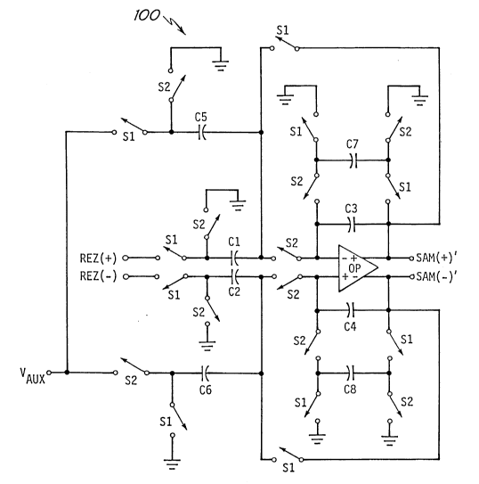
Fig. 5 is a schematic circuit diagram of a
fully differential sample and hold circuit to illustrate
a first embodiment of the invention. As clearly shown
in Fig. 5, circuit 100 includes only one operational
amplifier and no resistors, where the remaining
components are capacitors or switches. As explained in
detail below, circuit 100 permits adjustments of the
output in response to a single-ended input signal Vaux.
Therefore, circuit 100 is advantageous over circuit 10
in that it requires much less area in the semiconductor
medium and is more accurate.
In circuit 100, for ease of illustration,
capacitors Cl-C8 are assumed to have substantially the
same capacitance C. Sl indicates a group of switches
which are turned on at different times from the group S2
of switches. In the preferred embodiment illustrated in
Fig. 5, switches S1 are turned on when the clock signal
shown next to S1 in Fig. 2 and applied to S1 is high,
but are turned off when such clock signal is low.
Similarly, switches S2 of Fig. 5 are turned on when the
corresponding clock signal is high but are turned off
when such clock signal is low in Fig. 2. As shown in
Fig. 2, the clock signals for operating switches Sl, S2
do not overlap. As before, REZ(+), REZ(-) represent the
return to zero positive and negative input signals in
Fig. 5.
The operation of circuit loo is illustrated by
means of the schematic circuit diagrams in Figs. 6A-6D,
the table in Fig. 6D, and the timing diagram in Fig. 2.
At time T1, switches S1 are turned on and
switches S2 are turned off in Fig. 5 so that circuit 100
becomes the same as circuit lOOA in Fig. 6A. For
simplicity in description, identical components in the
figures of this application are labeled by the same
` 20270~3
- 10
reference symbols. For the purpose of discussion, it is
assumed that during the time period immediately before
time T1, the outputs SAM(+)' and SAM(-)' are at Vp, -Vp,
respectively, the inputs REZ(+), REZ(-) inputs at V, -V,
respectively, and a single-ended voltage Vaux is applied
to capacitor C5 as shown in Fig. 6A.
To simplify discussion, it is assumed that
capacitors Cl-C8 each has capacitance C. Therefore, the
electrical charges on the lefthand and righthand plates
of each of the eight capacitors are readily calculated
for circuit lOOA in Fig. 6A; the values of these charges
are listed in the table in Fig. 6D. During the time
period T2 in Fig. 2, all the switches Sl, S2 are open,
so that circuit 100 of Fig. 5 becomes circuit lOOB of
Fig. 6B. The opening of switches Sl does not cause any
current so that the electrical charges on both plates of
the eight capacitors retain the values shown in the
table of Fig. 6D.
During time T3, switches S2 are closed and
switches Sl are open, so that circuit 100 of Fig. 5
becomes the same as circuit lOOC of Fig. 6C. At time Tl
in reference to Fig. 6A, paths 102, 104 are connected
respectively to the outputs 116, 118 of amplifier OP.
During the time period T2, the two paths 102, 104 are
not connected to the amplifier at all. During time T3,
paths 102, 104 are connected to inputs 112, 114
respectively of the amplifier, instead of to the
outputs.
Due to the conservation of electrical charges,
the sum total of the electrical charges on the righthand
plates of capacitors C5, C1 and the lefthand plates of
capacitors C7, C3 will remain the same during the time
periods Tl, T2 and T3, since essentially no current
flows into or out of input 112 of the amplifier OP.
During time period Tl in reference to Fig. 6A, the sum
~ 2~7a83
..
total of electrical charges on the above-referenced
plates of capacitors Cl, C3, C5 and C7 are as follows:
C(Vp-V)+C(~V-Vp)+C(Vp-Vaux)+C(-Vp)=C(-V-Vaux+~V) (5)
During time period T3 in reference to Fig. 6C,
since the lefthand plates of capacitors C1 and C5 and
the righthand plate of capacitor C7 are grounded;
therefore, the electrical charges on the righthand
plates of capacitors Cl, C5 and the lefthand plate on
capacitor C7 are each C~V. Therefore, the electrical
charge on the lefthand plate of capacitor C3 is:
.
C(-V-Vaux+~V)-3C~V=C(-V-Vaux-2~V) (6)
The electrical charge on the righthand plate
of capacitor C3 is (V+Vaux+2~V). Hence the output
SAM(+)' is V+Vaux+3~V, since the amplifier OP adds
another offset voltage ~V. Similarly, according to the
table in Fig. 6D, the sum total of electrical charges on
the righthand plates of C2, C6 and on the lefthand
plates of C4, C8 at time Tl is:
C(-Vp+V)+C(~V+Vp)+C(-Vp)+C(Vp)=C(V+~V) (7)
During time period T3, charges on the
righthand plate of C2 and on the lefthand plate of C8
are each C~V and that on the righthand plate of
capacitor C6 is C(~V-Vaux), so that the lefthand plate
of C4 has an electrical charge whose value is:
C(V+~V)-2C~V-C(~V-Vaux)=C(V+Vaux-2~V) (8)
Thus the righthand plate of C4 has an
electrical charge whose value is -V-Vaux+2~V. The
` 2027083
.
12
output SAM(-)' is -V-Vaux+3~V, since the amplifier OP
introduces an additional offset voltage ~V.
Therefore, the potential difference between
the two outputs SAM(+)' and SAM(-)' is:
(V+Vaux+3~V)-(-V-Vaux+3~V)=2(V+Vaux) (9)
Hence circuit 100 in the above-described
operation permits the adjustment of the potential
difference between the two outputs by adding the
auxiliary voltage Vaux.
The above calculations will not be affected
significantly by the value of ~V becoming a large value
and the embodiment shown in Fig. 5 is offset
independent. If enough input power is applied to the
fully differential sample and hold circuit, circuit 100
of Fig. 5 can be further simplified in the form of
circuit 200 shown in Fig. 7, which is a schematic
circuit diagram of a fully differential sample and hold
circuit 200 to illustrate a second embodiment of the
lnventlon.
In comparison to circuit 100 in Fig. 5, the
switches to the left of capacitors C3, C7, C4 and C8
have been omitted and the lefthand plates of these
capacitors in circuit 200 are always connected to inputs
112 and 114 as shown in Fig. 7. Switches S1, S2 of
circuit 200 are operated by non-overlapping clocks S1,
S2 shown in Fig. 2, so that during times Tl, T2 and T3,
circuit 200 becomes respectively circuits 200A, 200B and
200C shown in Figs. 8A, 8B and 8C. In a similar manner,
the electrical charges on both plates of the eight
capacitors during time Tl may be calculated and are
listed in the table of Fig. 8D. During time T2, all the
switches are open, but the electrical charges on the two
plates of the eight capacitors retain their values so
2027083
.
that they are the same as those listed in the table in
Fig. 8D.
During time period T3, switches S2 are closed.
During this time, the electrical charges on the
righthand plates of capacitors C1, C5 and the lefthand
plate of capacitor C7 are each C~V. Again applying the
principle of conservation of electrical charges, the
electrical charge on the lefthand plate of capacitor C3
may be calculated in the same manner as before:
C(Vp-V)+C(~V-Vp)+c(Vp-Vaux)+c(~v-vp)-3cAV=
C ( -V-Vaux-AV) ( 10 )
Thus the electrical charge on the righthand
plate of capacitor C3 is V+Vaux+~V: the output SAM(+)
has the value V+Vaux+2~V, where an additional ~V is
introduced by amplifier OP.
Similarly, the electrical charge on the
rightha~d plate of capacitor C4 is given by:
C(-Vp+V)+C(~V+Vp)+C(-Vp)+C(~V+Vp)-2~V-C(~V-
Vaux)=C(V+Vaux-~V) (11)
Hence the charge on the lefthand plate of
capacitor C4 is -V-Vaux+~V; the output SAM(+)' has the
value -V-Vaux+2~V, where again the amplifier OP
introduces an additional offset voltage ~V. Hence the
potential difference between the two outputs is again
2(V+Vaux). Therefore, circuit 200 in the above-
described control system again permits the differential
output potential to be adjusted by adding Vaux thereto.
In comparison to circuit 100 of Fig. 5,
circuit 200 requires even fewer components and is
therefore even cheaper to manufacture.
Here, in deriving equations 5-11, we are
assuming that all the capacitances used have the same
~270g3
.
value C. However, the principle underlying this
invention can still be applied even when the
capacitances are different. In such event, the
potential difference between the outputs of the
operational amplifier is aV+bVaux, where a, b are
constants whose values are determined by the values of
the capacitances of capacitors C1-C8.
The invention has been described by reference
to particular embodiments. It will be understood that
various modifications may be made in the implementations
of the invention, the scope of which is limited only by
the appended claims.
.