Note: Descriptions are shown in the official language in which they were submitted.
2027 1 7 1
:,
PATENT
1335-33-00
TITLE: A CHEMICAL VAPOR DEPOSITION PROCESS TO ~EPLICATE
THE FINISH_AND FIGURE OF PRESHAPED STRUCTURES
This invention was made with Government support
- ,.,
under contract F33615-87-C-5227 awarded by the Air
Force. The Government has rights in this invention.
BACKGROUND OF THE INVENTION
~j
1. Field of the Invention
This invention relates to a process using chemical
vapor deposition for replicating, that is, making close
~ 10 copies of the finish and figure of preshaped structures.
-, The invention has particular utility in the rapid
fabrication Gf highly polished optics with only minor
polishing being required on the replica to obtain a
' final product, and with the original substrate or
; 15 mandrel being reusable. The invention also has utility
in the rapid fabrication of such products as ceramic
engine components and ceramic tubes.
l 2. DescriPtion of the Prior Art
:'
~i In the field of optics, light detection and ranging
(LIDAR) has come to be recognized as an important
',,.Y diagnostic tool for remote measurement of a diversity of
atmospheric parameters such as minor species
. .
,: .
2027 1 7 1
--2--
'
concentrations, pressure, temperature, and water vapor
profiles, aeroqol cloud distributions, and wind fields.
LIDAR techniques such as measurement of back scattered
signals, differential absorption, and Doppler shifts
have been used to obtain information about the earth's
atmosphere.
The performance of a LIDAR system depends upon the
j optical configuration of its receiving telescope.
Often, due to space limitations such as in a shuttle
borne LIDAR system, the length of the telescope is
fixed. Therefore, the optical designer must select a
; particular shape and optics speed of the mirrors to
maximize the throughput of the telescope. The most
critical element in the receiving telescope is the
primary mirror because of its size, weight, fabrication
cost, and thermal exposure to the outside world. Since
the received signal is directly proportional to the area
of the primary mirror, it is important to use as large a
~; primary mirror as feasible to obtain reasonable signal
levels for accurate measurement. This is particularly
~, true when a space-borne LIDAR system is used to measure
~i wind profiles in the troposphere on a global basis.
;~ The conventional techniques employed in the prior
. art for fabricating large (>1.0 meter diameter) mirrors
are ~uite slow and time consuming. Several months to
years are required to fabricate a large mirror from
ultra low expansion silica glass or "Zerodur" , a product
commercially available from Schott Glass Technologies,
Inc., 400 York Avenue, Duryea, PA 18462. Since a
number of space-based LIDAR systems are planned for the
future, considerable attention is currently being given
to the development of techniques for the rapid and
economic production of large, high performance mirrors.
* ~rad~mark
:
.,
:;
20~7171
.
--3--
A spin casting technique has been proposed to
fabricate 1.2 meter and 3.5 meter diameter glass mirror
blanks containing lightweight honeycomb cells. Although
this technique is relatively faster than the
conventional mirror fabrication methods and produces
lightweight mirrors, the weight of these mirrors is
~ still an order of magnitude more than permissible for
- many space applications. Further, the spin-casting
technique is unsuitable for fabricating large mirrors of
; 10 advanced ceramics such as silicon carbide (SiC),
titanium diboride (TiB2), and boron carbide (B4C) that
; have high melting points. These latter materials have
properties superior to those of glass for large
~ lightweight optics.
¦ 15 Other techniques involving the casting of fiber
reinforced composites containing epoxy and plastics and
;~ the stretching of membranes over appropriate substrates
' are also currently under investigation.
,~
j A process is disclosed in Canad~an Patent
Application No. 2,057,934 filed on December ~8,
i 1991, by J. T. Goela, M.A. Pic~erina and
^~ R. L. TaYlor and assigned to the assignee of the present
invention, for fabricating, by vapor deposition,
lightweight structures out of refractory materials. The
methods and lightweight structures disclosed in that patent
application involve a core made of qraphite to
i define the shape and size of each structure. The core
is coated with an appropriate deposit, such as SiC or
silicon (Si), to give the structure strength and
stiffness and for bonding thereof to another surface,
for example, the surface of a substrate comprising the
faceplate of a mirror being fabricated.
:,,
~'' .
:.
. . .
: .
2027 1 7 1
; -4-
In the fabrication of mirrors, it has been
proposed, as disclosed in the above mentioned Canadian
application for patent, to use graphite to form a
substrate or mandrel for replicating on a SiC faceplate.
On~ side of the mandrel is optically fabricated, either
as flat or as a convex spherical shape. The other side
of the mandrel is lapped flat. The lapped side of the
mandrel is bonded by means of pillars and graphite
cement to a baffle plate in a vapor deposition reactor.
The mandrel is then coated with multiple coats of a
suspension of carbon in solvent, following which the
- surface of the mandrel is buffed or polished to make it
as shiny as possible without significantly altering its
` figure. Deposition of silicon carbide on the mandrel is
~, 15 then effected. Without separating the faceplate from
~ the mandrel, the exposed silicon carbide surface may be
`~ etched with hot potassium hydroxide (KOH) to improve
bonding of graphite to silicon carbide. A lightweight
` structure core of graphite is then fabricated and bonded
3, 20 with graphite cement to the silicon carbide surface of
the mandrel. Silicon carbide is then chemically vapor
` deposited to enclose the core following which the baffle
plate is separa~ed from the baffle pillar~. Controlled
edging may be performed to remove excess silicon
carbide. Using a blade, the interface between the
graphite mandrel and the silicon carbide faceplate may
then be opened to recover the silicon carbide mirror
faceplate.
While this process disclosed in the aforementioned
Canadian Application No. 2,057,934 has advanced the
development of lightweight rapid optics fabrication
technology, the final product produced by the process is a
mirror blank that is not of the desired high optical quality,
that is, high finish, required for r-pace-based LIDAR systems.
~, 4
, ,:
: . .
',
. ,
,
-- 2 ~
, -5-
A reason for this is that graphite which is used for the
mandrel does not take a high polish. Additionally,
there is a substantial difference in the coefficients of
thermal expansion (CTE) between graphite and silicon
, 5 carbide. Graphite deforms substantially more than
silicon carbide at the high temperatures (about 1300C.)
at which deposition of silicon carbide in a chemical
vapor deposition reactor takes place. As a result,
replication of the ambient or room temperature figure of
a graphite substrate or mandrel by chemical vapor
` deposition of silicon carbide is not achievable in
practice. Compensation for the difference in
coefficients of thermal expansion is exceedingly
difficult to effect.
Thus, there is a need and a demand to provide a
rapid fabrication process to replicate with high optical
quality the finish and figure of preshaped optical and
~ other structures. The present invention was devised to
--~ fill the technological gap that has existed in the art~ 20 in these respects.
SUMMAR~ OF THE INVENTION
An object of the invention is to provide a chemical
vapor deposition process to replicate the finish and
figure of preshaped structures.
Another object of the invention is to provide a
process to replicate the very high finish and figure of
polished silicon carbide mirror substrates or mandrels
thereby to facilitate the rapid fabrication of mirrors
~, of high optical quality with only minor polishing of the
-~ 30 replica being required to obtain a final product.
.
:~;
''
~'
. .~ ,
,'`' ,
., ,
-6-
: A further object of the invention is to provide
such a process in which the original substrate or
.~ mandrel can be reused.
Still another object of the invention is to provide
an economical and facile process for the rapid
fabrication of preshaped structures by the use of
~` chemical vapor deposition in which the need for
compensation for differences in the coefficients of
' thermal expansion between the material of the original
: 10 substrate or mandrel employed and the material being
deposited on the mandrel to form the replica is avoided.
An additional object of the invention is to provide
` a chemical vapor deposition process to replicate the
finish and figure of a preshaped polished silicon
carbide substrate comprising the steps of:
(a) pretreating the substrate in situ by the
. deposition thereon of a thin carbon film of high
finish and uniform thickness; and
(b) forming a replica of the finish and figure
of the substrate by vapor depositing a layer of
silicon carbide of predetermined thickness on the
carbon film.
A further object of the invention is to provide a
process to replicate the finish and/or figure of
preshaped structures comprising the steps of:
(a) loading a polished preshaped substrate to
be replicated into a chemical vapor deposition furnace;
(b) evacuating, leak checking and then heating
:~ the chemical vapor deposition furnace;
(c) introducing gases into the furnace that
~ are operative at the temperature therein to cause a
:, thin carbon layer of high finish and uniform
'. thickness to be formed on the substrate;
.
~ '. c
.
-
~,;
.
:
2~1~7~71
,
,
(d) introducing gases into the furnace tocause the deposition of a layer of SiC onto the
carbon layer on the substrate, said layer of SiC
comprising a replica of the substrate; and
- 5 ~e) cooling the furnace to ambient
temperature, removing the substrate/replica, and
separating the substrate and replica.
îl In accomplishing these and other objectives, there
, has been provided, in accordance with the invention, a
' 10 chemical vapor deposition process to replicate the
finish and figure of highly polished silicon carbide
substrates or mandrels (for convenience, termed
~ substrates hereinafter~
: -,
In the operation of a chemical vapor deposition
apparatus, gases are introduced into a hot furnace or
~i reactor where they react at the walls of the furnace or
at the surface of a substrate or other structure loaded
into or placed in the furnace and form a solid deposit
or coating. For the deposition of SiC on the substrate,
methyltrichlorosilane (CH3SiC13, hereinafter referred to
as MTS), hydrogen (H2), and argon (Ar) gases are
introduced into the furnace through a stainless steel
, injector. Since MTS is a liquid at ambient or room
temperature, Ar is bubbled through the MTS liquid and
carries the MTS vapor above the liquid to the injector.
Gases that are unreacted-in the furnace are pumped out
by means of a vacuum pump, filtered, and cleaned in a
gas scrubber before being vented to the atmosphere.
By the use of this process, thick deposits (>0.25
~ 30 inch; 0.63 cm.) of SiC can be made. Typical conditions
;~ for the deposition of SiC are:
.: j
'.:,
' ~,
' ~
~-3
~:,
:~ ...
~ .
., .
.~
.
;: , 2~i7171
--8--
.,
Substrate temperature 1300C.
Furnace Pressure 200 torr
Partial pressure of gases - Ar68 torr
H2102 torr
MTS30 torr
In a first step of the replication process,
according to the invention, a polished preshaped
substrate is loaded into the chemical vapor deposition
furnace and heated to 1300C. In principle, the
substrate can be made from any material that has a
melting point that is higher than the deposition
temperature of the material being deposited. The finish
and/or figure replication of the substrate will be poor,
however, if the material of the substrate reacts with
the gases used in the replication process.
In a second step of the replication process, gases
are added into the chemical vapor deposition furnace
which form a thin carbon layer of film on the substrate,
which carbon layer or film is characterized in having a
high finish and uniform thickness. Three different gas
mixtures may be used to form such a carbon layer or film
for subsequent replication. These gas mixtures
`~ comprise:
-~ (l) MTS + Ar;
(2) Oxygen (2~ + Ar; and
(3) 2 + Ar followed by 2 + MTS + Ar.
Argon is used only as a carrier gas. The 2 source may
~; be special high purity air (i.e., 20% 2 and 80
nitrogen ( N2 ) -
In a third step in the replication process, SiC is
deposited onto the carbon film with the deposition
- continuing until a layer of SiC of desired thickness is
l obtained~
.,!,. ~
~ 'I
' ~,
` '~, , .
., ' .
. 2~7171
g
, In a fourth and final step, the furnace or reactor
is cooled to room temperature, the substrate/replica is
removed, and the substrate/replica separated. The
carbon layer allows for the easy separation of the
substrate and replica which otherwise would be bound
-~j tightly together.
!
' SiC replication may be achieved using the three
i different gas mixtures described above. The best
replication is obtained using the two-step pretreatment
process, 2 + Ar followed by 2 + MTS + Ar.
The general conditions under which the replication
occurs using the three gas mixtures are:
(1) MTS + Ar
Substrate temperature 1300C.
Furnace pressure 90.0 torr
Partial pressure of gases - Ar 78.7 torr
MTS 11.3 torr
Deposition time 10 min.
(2) 2 + Ar
Substrate temperature 1300C.
Furnace pressure 100-400 torr
Partial pressure of gases - Ar 98-32 torr
, 2 0.4-1.6 torr
Deposition time 5-15 min.
. .,
25 (3) 2 + Ar followed by 2 + MTS + Ar
First Step:
s Substrate temperature 1300C.
Furnace Pressure 200 torr
Partial pressure of gases - Ar 196 torr
`, 30 2 0.8 torr
Deposition time 4-5 min.
A
~..''
:.
2~2 7~71
--10--
Second SteP:
Substrate temperature 1300C.
Furnace pressure 200 torr
Partial pressure of gases - Ar 177-196 torr
2 0.8 torr
MTS 3-19 torr
Deposition time 2-5 min.
In the preferred embodiment of the invention, the
total flow of the various gases through the reaction
chamber of the chemical vapor deposition furnace is
maintained substantially constant during the in situ
pretreatment period and also the subsequent normal
chemical vapor deposition silicon carbide growth period.
Chemical vapor deposition onto a substrate which is
of the same material as that which is being deposited is
very advantageous. This is for the reason that with
such arrangement there is no coefficient of thermal
expansion difference for which compensation otherwise
would have to be provided to obtain a correct, that is,
! 20 a matching figure, on the replicated mirror. Thus,
replication of the ambient or room temperature figure of
a silicon carbide substrate may be effected
notwithstanding that the deposition of the chemically
vapor deposited SiC occurs at an elevated temperature
, 25 (1300C.). This is because there is no coefficient of
thermal compensation mismatch.
, The various features of novelty which characterize
` the invention are pointed out ~ith particularity in ~he
c claims annexed to and forming a part of this
specification~ For a better understanding of the
invention, its operating advantages, and specific
objects attained by its use, reference is made to the
accompanying drawings and descriptive matter in which
preferred embodiments of the invention are illustrated.
~ .
` 2al~7~1
Ll
, .
- BRIEF DESCRIPTION OF THE DRAWINGS
- With this description of the invention, a detailed description follows with reference being made to the
accompanying drawings which form part of the
specification, of which:
Fig. 1 is a schematic illustration of a chemical
vapor deposition apparatus that may be employed for the
pretreatment of a polished silicon carbide substrate and
also for the subsequent deposition thereon of a SiC
coating or layer in replicating the finish and figure of
the substrate;
Fig~ 2 schematically illustrates, in side view, a
~ SiC substrate having a polished upper surface;
,~
` Fig. 3 schematically illustrates, in side view, the
substrate of Fig. 2 after a first pretreatment of the
upper surface thereof with 2 and CH3SiC13 deposition
thereon of a thin carbon film;
Fig. 4 schematically illustrates, in side view, the
substrate of Fig. 3 after the chemical vapor deposition
~: 20 on the upper surface thereof of a replicating coating
;-3 or layer of SiC;
Fig. 5 schematically illustrates the separation of
the substrate and the replica of Fig. 4;
Fig. 6 shows a polished chemically vapor deposited
SiC substrate (left-hand side) and an as-deposited
: '
~s chemically vapor deposited silicon carbide mirror
- ~right-hand side) replicated therefrom;
Fig. 7 is a schematic illustration that is in
further explanation of the SiC replication process
accordin~ to the invention
:-
,
-" 2~2 ~171
-12-
Fig. 8 is a micrograph of the polished surface of a
chemically vapor deposited silicon carbide substrate
before deposition;
Fig. 9 is a micrograph of the surface of the
substrate of Fig. 8 after deposition; and
Fig. 10 is a micrograph of the replicated, as
deposited surface of the substrate of Fig. 8.
DESCRIPTION OF THE PREFERRED EMsoDIMENTs
,:
With respect to important properties of potential
`~ 10 large space-based optics materials, silicon carbide has
;~ been identified as the leading candidate based on the
excellent mechanical, thermal and physical properties
thereof, and additionally, existing evidence that large
: ,,
monolithic pieces of silicon carbide can be produced by
j 15 means of a chemical vapor deposition process.
`~, A scalable chemical vapor deposition process was
devised using MTS as a source for silicon carbide.
Chemical vapor deposited silicon carbide material was
~ produced and characterized for important physical,
;~ 20 mechanical, thermal and optical properties relevant to
large space-based optics. The chemically vapor
deposited silicon carbide is theoretically dense, single
phase (cubic), high purity, fine grained polycrystalline
~` material possessing high flexural strength (595 MPa),
,r 25 high thermal conductivity (198 Wm-lk~l), high elastic
~-- modulus (460 GPa), and excellent polishability
` (<10 A RMS).
The feasibility of replicating polished prefigured
silicon carbide mirrors directly by the chemical vapor
deposition process according to the invention was
demonstrated in small scale experiments in which
.
: `
-" 2027171
:`
-13-
polished silicon carbide mirror surfaces were produced
with only minor polishing of the replica being required
to obtain a final product, and with the original silicon
carbide substrate being reusable.
While in the preferred embodiment of the invention,
the polished original substrate which is to be
replicated is made of chemically vapor deposited SiC, it
j is to be understood that such silicon carbide substrate
may be formed by other methods that are known in the
art.
Figs. 2-5 of the drawings collectively provide an
illustrative explanation of the steps involved in the
replication of a silicon carbide mirror. Thus, Fig. 2
shows, in side view, a substrate having an upper surface
14 that is highly polished. The shape of the surface
~ may be flat or curved. When curved, the shape of the
4 surface 14 is the converse, that is, a "negative" of the
~-~ surface of the replica that is to be fabricated. For
example, if it is desired that the surface of the replica
have an inward curve, as in a concave mirror, the shape
of the polished surface 14 of the substrate 12 is so
`~ shaped as to have an outward curve, as in a convex mirror.
,. . ~,
O Fig. 3 shows the substrate 12 after the deposition,
in situ, on the polished surface 14 of a carbon film 16
~;~ 25 that has been deposited on the surface 14.
Fig. 4 shows the substrate after the deposition on
the carbon film 16 of a coating or layer 18 of SiC.
Fig. 5 shows the separation of the substrate 12 and
the layer or replica 18.
A feature of the invention is that the separation
of the substrate 12 and the replica 18 occurs without
the need for the application of foroe to pry them apart.
:
.
202 t~71
By the use of the process excellent replication of
chemically vapor deposited SiC onto the polished surface
of a substrate is obtained. This is demonstrated by
Fig. 6 which is a representation of a photograph of the
surface 14 of the polished chemically vapor deposited
silicon carbide substrate 12 (left-hand side of the
figure) and the surface 22 of an as-deposited chemical
vapor deposited silicon carbide mirror 20 (right-hand
side of the figure), replicated from the substrate 12,
reflecting an image (the letters "SiC") located in
front of the two surfaces 14 and 22.
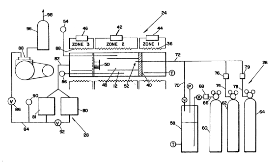
;-~ Fig. 1 schematically illustrates a chemical vapor
deposition apparatus 10 that may be used in accordance
~', with the invention for forming, in situ, carbon film 16
, 15 on the polished surface of the substrate that is to be
, replicated, such as the surface 14 of the substrate 12
,' of Figs. 2-5 described above, and for effecting the
~`~ deposition of a SiC layer 18 on top of the carbon film
16.
The chemical vapor deposition apparatus 10 includes
a horizontal research furnace 24 which may comprise an
' electrically heated 3-zone Lindberg furnace 24. The
apparatus 10 further includes a reactant supply system
26 and an exhaust system 28.
Associated with the furnace 24 is an elongated tube
30 of aluminum oxide (A12O3) containing a reaction or
deposition chamber 32 in which a substrate 12 to be
` replicated is placed. Tube 30 is substantially
coextensive with zone 2 of the 3-zone furnace 24. Zone
2 is heated by an electrical heating element 34. Zones
1 and 3 comprise manifold and exhaust zones,
respectively, and are heated by individually associated
` electrical heating elements 36 and 38. A manifold 40 is
provided at the interface of zones 1 and 2.
~'
~ `
2~2 ~71
-15-
A substrate temperature controller 42 controls the
~ energization of the heating element 34. Similarly, a
-~ manifold temperature controller 44 controls the
energization of the heating element 36 and an exhaust
temperature controller 46 controls the energization of
the heating element 38.
` Located within the deposition chamber 32 is a
deposition zone 48 in which the substrate 12 is placed.
The substrate 12 in Fig. 1 is shown as consisting of
~;, 10 four sides of an open box. Also included in the
deposition chamber 32 is a baffle plate 50. An injector
52 made of stainless steel extends through the mainfold
40 into the deposition zone 48. The pressure and
temperature within the zone 48 are indicated by a
pressure gauge 54 and a temperature gauge 56,
respectively.
The reactant supply system 26 includes a bubbler
cylinder and dip tube device 58 containing MTS, a tank
, 60 comprising a source of argon under pressure, a tank
62 comprising a source of hydrogen under pressure, and a
tank 64 containing a source of purified or "special" air
(20% 2 and 80% N2) under pressure. ~rgon flows through
a flow line 66 to the bubbler cylinder and dip tube
device 58. A mass flowmeter and controller 68 connected
in the flow line 66 controls the flow of argon.
Argon bubbles carrying the reagent MTS flow through
flow lines 70 and 72 to the injector 52 at the manifold
40. Hydrogen flows from tank 62 through a flow line 74,
in which a ~ass flowmeter and controller 76 is
ccnnected, to the junction of flow lines 70 and 72 and
through flow line 72 to the iniector 52. Air flows
from tank 64 through a flow line 78, in which a mass
flowmeter and controller 79 are connected, to the
:~,
''
.
2~7171
-16-
junction of flow lines 70 and 72, and through the flow
line 72 to the injector 52.
The exhaust system 28 includes a pair of gaseous
-~ filters 80 and 81 that are connected by a flow line 82
to the exhaust zone of the furnace 24. A flow line 84,
;, in which a furnace pressure control valve 86 is
-~ included, connects the outputs of filters 80 and 81 to a
, vacuum pump 88. The output pressure in flow line 84 is
', indicated by a pressure gauge 90. A by-pass valve 92
may be connected between the outputs of filters 80 and
, 81, as shown. The output of vacuum pump 88 is connected
".
, by a flow line 94 to a gas scrubber 96. The output of
the gas scrubber 96 is connected by a flow line 98
~, through which the scrubbed gases are vented to the
atmosphere. The exhaust system 28 is provided to
evacuate the gaseous reaction products that are released
~jl, in the reaction chamber 48 during the pretreatment and
;'', silicon carbide deposition processes.
' '1
The SiC material to be deposited on a substrate 12
in the deposition chamber 48, as previously mentioned,
is fabricated by reacting MTS with H2. Other silane and
,~ hydrogen sources can be used, however, to form SiC.
This material has been fabricated over a wide range of
deposition temperature and reactor pressure, that is,
' 25 pressure in the furnace reaction chamber 48, as shown in
Z Table I below:
TABLE I
~,' Flow Rates Deposi- Deposi-
, *(Slpm)tlon Reactor tlon
,~ 30 Material Temper- Pressure/ Ra,t,e
i _e~Q~9SÇ~ _@2_ ~H~S~Ç~3 Ar _a~YE~ S~ torr ~m~
_
SiC <10 <2 <4 1358_ 25-300 S3 5
~i, *Standard liters per minute
.~ .
.
. . ~
2~2i~71
; -17-
The reagents are introduced into the reaction
- chamber 48 through the injector 52 which, as shown, is
centrally located. While not shown, the injector 52 may
be cooled with water to prevent deposition in the
; 5 injector 52, and to keep the temperature of the reagents
low thereby minimizing gas phase decomposition or
nucleation. The deposition thickness is controlled by
varying the deposition process parameters and the
- deposition time. After a sufficient thickness of the
SiC material has been deposited, the deposition process
is terminated and the furnace is cooled down very slowly
to minimize any tendency to cracking of the replicated
structure due to residual stresses.
The replication of a polished silicon carbide
~1 15 substrate, in accordance with the invention, involves,
prior to the deposition of the silicon carbide replica,
the deposition at 1300C. of a thin carbon layer or film
on the polished surface of the substrate to be
, replicated. The carbon film deposited in such
pretreatment step allows for the substrate and the
replica to be easily separated after the silicon carbide
deposition. Upon separation, the carbon film adheres to
the surface of the replica. The as-separated surface of
the replica has the high finish and figure matching the
finish and figure of the substrate.
~- The carbon film can be deposited using several
j different gas mixtures: (1) MTS; (2) air; and (3) air
~, MTS. By using air as a reactant the polished surface of
the substrate, in effect, is treated with oxygen. In
a preferred embodiment of the invention which has
produced the best replication results, the substrate is
first treated in situ with air for five (5) minutes
followed immediately by a treatment of air plus
methyltrichlorosilane for three (3) minutes. The
!.
."
,,
:. ` i ~,
..
'
2~'7~71
::'
-18-
conditions required for deposition of silicon carbide
were then initiated and continued for thirty (30) hours.
A summary of the chemical vapor deposition
conditions to achieve silicon carbide replication, in
accordance with the two-step pretreatment process of the
preferred embodiment of the invention, are given in
Table II.
T~LB II
- 10strete Furnace Gas Flow tes ~Sl m)
Tem~. Pressure F ~ PDeposition
(C.~ (mm. Hg) MTS Ar H2 AirTime
' ~'' . ........... _ . ..
1300 200 -0- 5.0 -0- 0.1 5 min.
1300 200 0.45 5.0 -0- 0.1 3 min.
151300 200 0.70 2.0 3.0 -0- 30 hrs.
The schematic illustration of Fig. 7 provides in
greater detail an explanation of the silicon carbide
replication process of the invention. As there shown, a
carbon rich silicon carbide film 100 is first deposited
~-~ 20 on a polished silicon carbide substrate 102 and then a
layer 104 of chemically vapor deposited SiC is grown
- over the film 100. At the end of the deposition, the
replicated SiC 104 is easily separated from the
substrate 102. This is because of the weak bond between
~, 25 the film 100 and the silicon carbide 104. Good
replication is achieved by making the film very thin.
It is believed that the thinner the film the better the
.;
; replication. Irrespective of the validity of this
~; hypothesis, excellent replication has been achieved
with the thickness of the film 100 in this range.
The substrate and replica surfaces produced in
experiments with the different gas mixtures were
characterized using a variety of techniques. From such
r
2~7171
' ; -1 9-
characterization studies, some information about the
replication process was obtained. First, the air or 2
;~ + Ar pretreatment produces a thin silicon dioxide
(SiO2) film on the SiC substrate. Second, a carbon
layer is deposited as a result of the MTS + Ar and 2 +
; MTS + Ar treatments. The data indicates that this
carbon has a high finish and is in the form of a glassy
carbon or incomplete graphitized carbon. The oxygen
i most likely promotes the disassociation of the MTS and
j 10 the formation of a shiny carbon film (as compared to the
less bright carbon surface formed using MTS + Ar alone),
although the chemical mechanism is not understood. For
the two-step process, 2 + Ar followed by 2 + MTS + Ar,
the thickness of the SiO2 film (produced during the 2 +
Ar step) ranged from 0.006-0.036 ym (60-360 A) and the
carbon film (produced during the 2 + MTS + Ar step)
` ranged from 0.22 to 1.00 ~um (2200-10000 A), respectively.
The following Examples are intended to be
illustrative and not be limiting in any way.
EXAMPLE I
The chemical vapor deposition apparatus of Fig. 1
was used to pretreat in situ and to obtain a silicon
carbide deposit from MTS using the process conditions
according to the preferred embodiment of the invention
as set forth in TABLE II. Four (4) 1.5 inch (38 mm.)
diameter polished silicon carbide substrates were placed
in the reaction region or zone 48 prior to pretreatment
and deposition of SiC. The substrates were each mounted
in an individually associated holder made of graphite.
- 30 After deposition for 30 hours, followed by cool-down,
each as-deposited silicon carbide replica easily
separated from its associated silicon carbide substrate.
Finish and figure for each of the replica~ matched the
finish and figure of the original polished silicon
carbide substrate individual thereto.
,.
.~ ,
2~7~1
-20-
EXAMPLE II
The chemical vapor deposition apparatus of Fig. 1
` was used to pretreat in situ and to obtain a silicon
carbide deposit from CH3SiC13 on four 1.5 inch (38 mm.)
diameter polished silicon carbide substrates mounted
` similarly to the substrates of Example I, with the
temperature of the substrates maintained at 1300C.
during both the pretreatment and silicon carbide growth
stages. In the pretreatment stage which was of fifteen
tl5) minutes duration, the furnace pressure was 100 mm.
Hg. The flow of argon and air were at the rates of 5
and 0.1 standard liters per minute, respectively, while
the flow of MTS and H2 were zero. In the silicon
carbide growth stage which continued for 27 hours, the
furnace pressure was 200 mm. Hg and the flow of MTS, Ar
and H2 were 0.70, 2.0 and 3.0 standard liters per
minute, respectively. The flow of air was zero. With
the~e conditions and deposition times, after deposition
for 27 hours followed by cool-down, the as-deposited
silicon carbide partially adhered to the silicon carbide
substrates, i.e., separation of the replicas was
achieved in two only of the four substrates.
. ~
EXAMP~E III
The chemical vapor deposition apparatus of Fig. 1
was used to pretreat in situ and to obtain silicon
carbide deposit from MTS on four 1.5 inch (38 mm.)
polished silicon carbide substrates, mounted similarly
to the substrates in Example I, with the temperature of
. the substrates maintained at 1300C. during both the
pretreatment and silicon carbide growth stages. In the
pretreatment stage which was of five (5) minutes
duration, the furnace pressure was 400 mm. Hg. The
flows of Ar and air were at the rates of 5 and 0.1
~tanderd liters per minute, respectively, while the ilow
2~127171
-21-
:
of MTS and H2 were zero. In the silicon carbide growth
` stage, which continued for 36 hours, the furnace
pressure was 200 mm. Hg and the flow of MTS, Ar and H2
were 0.70, 2.0 and 3.0 standard liters per minute,
respectively. After deposition for 36 hours, followed
by cool-down, under these conditions, the as-deposited
SiC partially adhered to the silicon carbide substrates,
i.e., sections of some of the as-deposited silicon
carbide replicas separated.
EXAMPLE IV
~,
The chemical vapor deposition apparatus of Fig. 1
; was used to pretreat in situ and to obtain a silicon
,~ carbide deposit from MTS on a 1.5 inch (38 mm.) polished
silicon carbide substrate mounted similarly to the
substrate of Example I with the temperature of the
substrate maintained at 1300C. during both the
?
pretreatment and silicon carbide growth stages. In the
pretreatment stage which was of five (5 ? minutes
duration, the furnace pressure was 200 mm. Hg. The flow
lj 20 of Ar and air were, respectively, 5 and 0.10 standard
i liters per minute, with the flow of CH3SiC13 and H2
being zero. In the silicon carbide growth stage, which
was of 40 hours duration, the furnace pressure was
1 maintained at 200 mm. Hg and the flow of MTS, Ar and H2
¦ 25 were 0.70, 2.0 and 3.0 standard liters per minute,
respectively, with the flow of air being zero. After
deposition and cool-down, the as-deposited silicon
carbide replica was easily separated from the substrate,
i.e., they simply fell apart when the furnace 24 was
disassembled at the end of the run. Figs. 8 and 10 of
the drawings show micrographs, respectively, of the
silicon carbide substrate surface before deposition, the
substrate surface after the deposition, and the
replicated, as-deposited surface of the replica.
:,
.
- 2~27~71
.
-22-
Magnification is 200X. Notice that the post-deposition
substrate surface and the replicated, as-deposited
surfaces are very similar and have surface features
` which are <5 ~m. The predeposition substrate surface
(Fig. 8) appears to be smoother (having fewer features)
;~ than the post-deposition surface and replicated surface.
,:
EXAMPLE V
The chemical vapor deposition apparatus of Fig. 1
was used to pretreat in situ and to obtain a silicon
carbide deposit from MTS on a 1.5 inch (38 mm.) polished
silicon carbide mounted similarly to the substrates of
Example I, with the temperature of the substrate
`~ maintained at 1300~. during both the pretreatment and
silicon carbide growth stages. In the pretreatment
stage which was of five (5) minutes duration, the
`~ furnace pressure was 100 mm. Hg. The flow of Ar and air
were, respectively, 5 and 0.1 standard liters per minute
with the flow of MTS and H2 being zero. In the silicon
~ carbide growth stage, which was of 16 hours duration,
'r, 20 the furnace pressure was 200 mm. Hg and the flows of
MTS, H2 and Ar were 0.70, 2.0 and 3.0 standard liters
per minute, respectively. The flow of air was zero.
The as-deposited silicon carbide adhered to the silicon
carbide substrates.
Summarizing the replication results, in situ
oxygen etch alone appears to be sufficient to achieve
replication. Analysis indicates that an oxide layer
(SiO2) forms on the polished silicon carbide substrate
when it is exposed to oxygen at high temperature
(1300C.) and that this oxide layer acts as a catalyst
to form a graphitic carbon layer upon reaction thereof
with MTS during initial deposition of silicon carbide.
By controlling the thickness of the oxide layer the
~;~ thickness of the graphitic carbon layer and thus the
~,'
~ '
.
. . .
,:
`` 20~7171
-23-
degree of replication can be controlled. As mentioned
hereinbefore, however, the best replication was obtained
using the two-step process previously described herein:
2 + Ar followed by 2 + MTS + Ar.
Thus, there has been provided, in accordance with
s the invention, a chemical vapor deposition process for
3 replicating the finish and figure of preshaped
structures. The process of the invention has especial
utility in the replication of the very high finish and
figure of polished silicon carbide mirror substrates or
-~j mandrels and enables the ràpid fabrication directly of
-~ mirrors of high optical quality, that is, high finish
with only minor polishing of the replica being required
t to obtain the desired final product.
.,3
The process of the invention is characterized in
the avoidance of any need for compensation for
differences in the coefficients of thermal expansion
between the material of the substrate or mandrel and the
' material being chemically vapor deposited thereon to
~; 20 fabricate a replica. The procesæ is further
characterized in that the original substrate or mandrel
is reusable.
With this description of the invention in detail,
those skilled in the art will appreciate that
modifications may be made to the invention without
departing from the spirit thereof. Therefore, it is not
intended tha~ the scope of the invention be limited to
the specific embodiments illustrated and described.
-,
: ~,
i
:''
' ',.-: