Note: Descriptions are shown in the official language in which they were submitted.
2~2~3~
VARYING BANDWIDTH DIGITAL SIGNAL DETECTOR
Field of the Invention
The invention relates to radio frequency co~ unication and, more
particularly, to digital signal transmitter and receiver arrangements.
5 Back~round of the Invention
In RF digital comm~lnication systems, the bandwidth of a channel is
generally preset in accordance with the permitted frequency spectrum rather thanchosen on the basis of the data charact.-ri~tics Once the channel bandwidth is
known, the data rate and the shape of the digital signal may be selected so that the
10 p~",lilled frequency spectrum is not exceeded. It has also been necessary to avoid
nonlinearity in transmission which could cause the RF spectrum of the signal to spill
over the assigned channel bandwidth.
Techniques have been devised to optimize signal reception by
controlling the bandwidth of a receiver. In some arrangements, the bandwidth is
15 varied in accordance with the signal to noise ratio. U.S. Patent 4,189,755 issued to
M. S. Balbes et al, February 19, 1980, discloses a television receiver thresholdextension system in which the received video signal and noise are sampled and
signal representative of the signal to noise ratio is formed. When the received signal
drops to an objectionable level, the bandwidth of the receiver is narrowed to reduce
20 the signal noise.
U.S. Patent 4,792,993 issued to J. Y. Ma, December 20, 1988, discloses
a receiver system having automatic bandwidth adjustment for signals with varyingbandwidths. A bandwidth detection circuit indicative of the bandwidth generates a
filter bandwidth control signal which selects one of a plurality of b~n(lp~s filters to
25 accommodate the incoming signal.
Some arrangements vary receiver bandwidth in accordance with
amplitude of the received signal. U.S. Patent 3,904,968 issued to B. M. Brinegar,
September 9, 1975, for example, discloses a signal sensitive switching circuit that
allow normal operation of a receiver when the received signal is greater than a
30 predetermined amplitude and inserts a narrow band filter to reduce the effects of
noise when the received signal is less than the predetermined amplitude.
With respect to data signals, U.S. Patent 4,045,740 issued to K. L.
Baker, August 30, 1977, discloses a method of optimizing the bandwidth of a radio
receiver to accommodate signals having widely varying data rates wherein the
35 oplilllulll intermP~ te frequency for a given data rate is determined and a filter
having a continuously tunable bandwidth is adjusted accordingly.
~g ~
~0~36~f-
- 2 -
As is well known in the arl, signal detection for data occurs
between transitions of the demodulated data waveform. The receiver
bandwidth, however, is generally set to accommodate the wide frequency
spectrum of the transitions and may be varied as aforementioned in accordance
5 with the amplitude or signal to noise ratio of the received signal. As a result of
the wide bandwidth to accommodate transitions, the noise remains at a high at
the detection instants. This noise due to transition determined bandwidth
results in lower detection accuracy. It is an object of the invention to providean improved digital signal transmission arrangement having more accurate
10 detection without limiting the data transition rate.
Brief Summary of the Invention
The foregoing object is achieved by recognizing that a wide
bandwidth is required only for data transi~ions but a narrow bandwidth is
sufficient to distinguish between signal levels at detection instants. A wide
15 band data signal is transmitted to accommodate fast transitions. Data
detection is improved by providing a wide bandwidth for received data
transitions and a narrow bandwidth at deleclion instants to minimi7e the effectsof noise and other interference.
The invention is directed to a communication system in which at
20 last one carrier modulated by a first information signal is received. The first
information signal has a plurality of levels and transitions between the levels
occurring at predetermined intervals. A demodulated signal corresponding to
the first information signal is formed. The levels of the demodulated signal
between transitions are detected at a narrow bandwidth by limiting the
25 demodulated signal to a first bandwidth at the transition instants of the first
information signal and to a second narrower bandwidth between the transitions
and sampling the baseband signal from lhe bandwidth limiting means at the
narrower bandwidth.
In accordance with one aspect of the invention there is provided
30 a communication receiver comprising: means for receiving a modulated RF
signal including at least one carrier signal modulated by a first information
signal, the first information signal having a plurality of levels and transitions
between the levels occurring at predetermined inlervals~ means responsive to
. ~
~ b
'? 3 ~ ~f
- 2a -
the received modulated RF signal for forming a demodulated signal including a
component corresponding to the first information signal, and means for
detecting the levels of the demodulaLed signal between the transitions of the
first information signal, the dc tecting mcilns including: means for limiting the
S demodulated signal to a first bandwid~h al the transition instants of the first
information signal and to a second narrower bandwidth between the transitions
of the first information signal, and means for sampling the demodulated signal
from the bandwidth limiting means during ~he second narrower bandwidth of
the demodulated signal.
10 Description of the Drawin~
FIG. 1 is a block diagram of a plurality of data transmitters in a
communication system illustrative of the invention;
FIG. 2 shows waveforms illustrating the frequency bands
assigned to the transmitters of FIG. l;
FIG. 3 is a block diagram of a data receiver according to the
prior art;
FIG. 4 is a block diagram ol a data receiver illustrative of the
invention;
FIG. 5 shows waveforms that illustrate the operation of the data
20 receiver of FIG. 4; and
~ ':
2 Q ~
FIG. 6 shows a block diagram of a switched capacitor filter that may be
used as the time varying filter in the circuit of FIG. 3.
Detailed Des~ ti~n
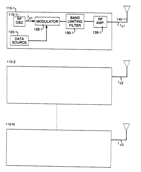
Referring to FM. 1, there is shown a set of data tran~ e~s 110-1,
5 110-2, ..., l lO-N in a colllmullication system illustrative of the invention. Data
tr~n~mitter 110-1 comprises RF oscillator 115-1, data source 120-1, modulator
125-1, band limiting filter 130-1, RF amplifier 135-1 and antenna 140-1.
RF oscill:~tQr 115-1 and data source 120-1 have their outputs connected to the
oscillator and data inputs of modulator 125-1. The output of modulator 125-1 is
10 connected through band limiting filter 130-1 to the input of RF amplifier 135-1 and
the RF amplifier output is in turn connected to tr~nsmitting antenna 140-1.
In FIG. 1, RF oscillator 115- 1 generates a carrier signal at a
predetcerminçd frequency fCl. Data source 120-1 supplies data signals having one of
two or more levels between successive transitions determined by a data clock
15 therein. Modulator 125-1 combines the data signals from data source 120-1 with the
carrier frequency signal fCl to form a data modulated signal having a predetermined
bandwidth centered at the carrier frequency. Modulator 125-1 may implement any
of the well known modulation techniques such as amplitude, frequency or phase
mod~ tion. Data trans~ els 110-2 through l lO-N are substantially similar to data
20 tr~n~mittçr 110-1 except that the carrier frequency of each of tr~n~mitters 110-1,
110-2, ..., l lO-N is different.
In priorly known co,,,,,,llnic~tion systems using carrier frequency
assignment, each data tr~nimittçr is assigned a carrier frequency and the band
limiting filter is set so that the modulated signals from the different data tr~nsmitters
25 do not overlap. FIG. 2 illustrates carrier frequency and channel band assignments
for the transmitter arrangement of FIG. 1. Referring to FIG. 2, waveform 201 shows
a frequency spectrum arrangement in which channel bands are separated to avoid
interference between channels.
Transmitter 110-1 of FIG. 1 uses channel 205-1 having a center
30 frequency of fCl . Band limiting filter 130-1 is set to limit the band between lower
frequency limit fLl and high frequency limit fHl as indicated by bracket 225-1.
Tr~nimitter 110-2 occupies channel 205-2 with a center frequency of fc2~ low limit
frequency fL2 and high frequency limit fH2 as indicated by bracket 225-2 and
transmitter l lO-N occupies channel 205-N with a center frequency of fCN~ low limit
35 frequency fLN and high limit frequency fHN as in(lic~tçd by bracket 225-N. The
tr~n.~mittçr channels are non-overlapping and generally are separated by guard
2~?3~4
bands.
FM. 3 shows a priorly known data receiver 300 that may be used to
recover the data signals from channels arranged according to waveform 201 of
FIG. 2. Assume for purpose of illustration that receiver 300 is adapted to detect
S phase modulated signals. The data receiver of FIG. 3 comprises antenna 301, mixer
303 adapted to convert received RF signals to baseband, local oscillator 315, band
limiting filter 305, data signal sampling detector 310, automatic frequency control
320, data clock 330, and timing control 325. Referring to FIG. 3, a signal having a
prescribed carrier frequency, e.g., fCl, is received by antenna 301 and sent to mixer
10 303. The output of local oscillator 315 is combined with the received signal in mixer
303 to translate the received signal to baseband. Filter 305 is of the low pass type
having a fixed b:~ndpa~s that removes high frequency components of the baseband
signal applied thereto. The filter output is a signal representative of the phase
variations corresponding to the data signal component of the received signal. The
lS phase varying representative signal is applied to sampling detector 310 wherein it is
periodically sampled. Data signal sampling instants are controlled by the feedback
loop including data clock 330 and timing control 325 and the frequency of the local
oscillator output signal is controlled by automatic frequency control 320 as is well
known in the art.
Referring again to FIG. 2, the bandwidth of each channel of waveform
201 is fixed. Therefore the bandwidth of filter 305 is set to adequately pass the data
signals and to limit noise. Waveform 210 illustrates the frequency ~signm~nts ofchannel arrangement in accordance with the invention. Each channel has a center
frequency that is separated from the center frequencies of the other channels. The
bands occupied by the channels overlap. Tr~n~mitter 110- 1 of FIG. 1 has its carrier
frequency fCl separated from the carrier frequency fc2 of tran~mitter 110-2 and from
the carrier frequency fCN of tr~n~mitter l lO-N as in~lic~te~l in waveform 210. The
carrier frequency separation may be substantially smaller than in waveform 201. As
in(1ir~te~1 in waveform 210, the bandwidth of a channel varies over a data interval.
30 At the transition times, the bandwidth for each channel is wide and covers a
si~nific~nt portion of the total band for the channels. Between transition times,
however, the data signal is at a single level and the bandwidth is narrow. For
example, the band for the signal of carrier fCl shown as curve 215 extends from FL
to FH1 at transition times as indicated by bracket 230- 1 but is very narrow (curve
35 220) around carrier frequency fCl in the level portions of the data signal.
2 ~?~ 6~
The bandwidth of each channel in waveform 210 at the transition times
is much wider than the channel bandwidths in waveform 201 so that the ch~nnel
bands at transition times overlap. The band for transmitter 110- 1 extends from low
frequency limit fLl to high frequency limit fHl and overlaps the band for tr~n~mitter
5 110-2 which extends from low frequency limit fL2 to high frequency limit fH2.
Similarly, the band for tr~n.~mitt~r l lO-N extends from low frequency limit fLN to
high frequency limit fHN as indicated by bracket 230-N. The wide overlapping
channel bandwidths occurring only at transition times of the modulating digital
signals accommodate much faster data transitions. The overlap of other channels
10 results in signal interference that prevents successful recovery of the data in the prior
art receiver 300. The bandwidth for a channel in the level portions of the digital
signal, however, is narrow. According to the invention, a receiver is synchroniæd to
a particular carrier frequency, e.g., fCl . The received signal is demodulated and the
demodulated signal is passed through a time varying filter that is synchronized to the
15 data signal mocl~ ting the particular carrier. At transition times of the data signal
modulating the particular carrier, the bandwidth of the time varying filter is set to
accommodate the transition occurring thereat. The bandwidth is reduced between
tr~n~ition times of the data signal modulating the particular carrier so that noise and
inlelrelellce is minimi7ed and the level can be accurately sampled.
FIG. 4 shows a data receiver embodiment 400 of the invention which is
adapted to accurately recover data transmitted in an overlapping channel
arrangement such as illustrated in waveform 210. FIG. 5 shows waveforms
illustrating the operation of receiver 400. Data receiver 400 comprises antenna 401,
mixer 403, time varying filter 405, sampling detector 410, local oscillator 415,automatic frequency control 420, data clock 430, timing control 425 and filter
bandwidth control 440. The sample detector 410, the data clock 430, timing control
425 and automatic frequency control 420 may be analog or digital circuits well
known in the art. If such circuits are digital, sample detector 410 includes an analog
to digital converter at its input and timing control 425 and automatic frequency30 control 420 include digital to analog converters at their outputs.
Referring to FM. 4, a signal including a phase modulated component
having a prescribed carrier frequency, e.g., fCl, is received by antenna 401.
Waveform 501 of FIG. 5 illustrates a data signal while waveform 505 shows a phase
mod~ ted carrier modulated by the data signal of waveform 501. Local oscillator
35 415 generates a local fCl carrier so that phase modulated component for the fcarrier is tr~n~l~ted to baseband in mixer 403. The output of mixer 403 has a
- 20q7~4
component representative of the phase of the data signal mod~ ting the fCl carrier
but includes many other components related to the wide band t~n~missions from
other sources. Components other than the prescribed phase modlll~ted component
constitute interfering noise.
Time varying filter 405 receives the baseband signal from mixer 403.
After setting of the local oscill~tor frequency and synchronization of the data signals
as will be described, the bandwidth of filter 405 is varied during each data signal
period. At data transition times, the bandwidth of filter 405 is extended to
accommodate the high frequency components of the transition. The bandwidth of
10 filter 405 is narrowed between transition times to limit the noise in the signal from
mixer 403. Filter 405 may comprise a switched capacitor low pass filter having
controllable Q and controllable bandwidth. The time variation in Q and bandwidthmay be achieved by altering the switched c~p~cit()r clock frequency or by modifying
the values of switched capacitor elements as is well known in the art.
Waveform 507 shows an exponentially decreasing signal applied to the
control input of filter 405 from filter bandwidth control 440. In each data signal
period, the control signal decreases from a value that causes the filter to pass the
entire band of the received signal having the fC1 ca~ier to a value that passes only a
narrow portion of the band centered at carrier frequency fCl . At each transition time,
20 e.g., tl, waveform 507 is high and filter 405 is set to a wide bandwidth so that it
passes the data signal tr~n~ition without distortion. From time tl until the next
transition time t2, the control signal in waveform 507 decreases. As a result, the
bandwidth of filter 405 at time tl is adequate for the data transition but also passes
components of the received signal related to other tr~nsmi~ions of the
25 co---",llniç~tion system and noise. The bandwidth just before time t2 is narrow so
that the components due to other tr~n~missions and noise are removed by filter 405.
It is to be understood that other waveshapes such as square or linearly decreasing
waveforms may be used to optimiæ the time varying filter action to transfer digital
signal transitions without distortion and to minimi7e noise and interference at
30 sampling instants during the level portions of the digital signal.
Waveform 510 illustrates the output of time varying filter 405 for a
sequence of data signal periods. The filter output signal in waveform 510 at thebeginning of each data period may assume any value since the received signal hasmany interfering colllpollents and the bandwidth of the filter is wide so that all such
35 components pass through the filter. At transition times tl and t4, the value of
waveform 510 is relatively high while the value of the waveform is relatively low at
- 2~27364
transition times t2, t3, tS and t6. The state of waveform 510 at transition times
depends on the noize and interference present in the demodulated signal applied to
filter 405. Since the bandwidth of filter 405 is narrow just before a transition time,
only a small portion of the data signal band for carrier frequency fCl is passed.
5 Consequently, the filter output represents the value of the fCl data signal and there is
little noise present.
Time varying filter 405 in FM. 4 may comprise the switched capacitor
filter arrangement shown in FIG. 6. Referring to FIG. 6, the switched capacitor filter
comprises input terminal 601, trancmi~ion gates 605, 610 and 615, switched
10 capacitor 607, amplifier 620, integrator capacitor 625 and voltage controlledoscillator 630. Received baseband signal RBS from mixer 403 in FIG. 4 is appliedto input terminal 601. As is well known in the art, switched capacitor 607 and
transmi~sion gates 605, 610 and 615 form a resistive charging source for integrator
capacitor 625. This resistive charging source is varied by changing the frequency of
15 the clock outputs of voltage controlled oscillator 630. As a result, the pass band of
the filter is a function of the clock frequency.
Voltage controlled oscillator 630 provides the clock signal CLl for
tran~mi~sion gates 605 and 610 and the clock signal CL2 for tran~mi~sion gate 615.
Clocks CLl and CL2 are non-overlapping square waves occurring at the frequency
20 dete~nin~d by voltage controlled oscillator 630. When clock CLl turns transmi~sion
gates 605 and 610 on, switched capacitor 607 is charged to the voltage from the bias
source including resistors 635 and 640 and capacitor 645. When clock CL2 turns on
the signal RBS is transferred through capacitor 607 and tran~mi~sion gate 615 to the
input of integrating operational amplifier 620. The ,nil~i,nll", clock frequency is
25 selected to be much higher than the frequency components of the desired baseband
input to the filter.
As is well known in the art, the frequency of oscillator 630 is
determined by the control voltage signal FBC applied to its input. Signal FBC isshown in waveform 507 of FIG. 5. During each data signal period, e.g., between
30 times tl and t2, the control voltage decreases from a high value to a low value and
the clock signal frequency in FIG. 6 decreases from a high value to a low value. At
time tl, the resistance exhibited by switched capacitor 607 is relatively small and
increases to a m~ lum just prior to time t2. Consequently, the bandwidth of the
switched capacitor filter of FIG. 6 decreases from a maximum value at transition35 time tl to a Illini,,,l.... just prior to transition time t2.
~o~73~
Sampling detector 410 receives the output of time varying filter 405 and
is opel~ive to sample the each data signal theltrlulll at time determined by data
clock 430 and timing control 425. Waveform 515 of FIG. S illustrates the pulses
from data clock 430 and waveform 520 illustrates the sampling pulses from timing5 control 425. These sampling pulses are set to occur when the bandwidth of timevarying filter 405 is narrow so that the effect of interference components and noise is
minimi71xl In FIG. 5, the sampling pulses in waveform 520 occur just prior to the
transition times defined by the data clock pulses of waveform 515. Waveform 525
illustrates the output of sampling detector 410. The data detector output signal in
10 waveform 525 between times t2 and t3 corresponds to the positive polarity of the
level of the data signal of waveform 501 in the interval between times tl and t2sampled just prior to time t2. The sample detector outputs for the data signal periods
of waveform 501 between times t3 and t4 and times t5 and t6 correspond to the
positive levels of the data signals in those intervals while the sample detector outputs
15 in waveform 525 for the data signal periods of waveform 501 between times t2 and
t3 and times t4 and tS correspond to the negative levels of the data signals of
waveform 501 in those intervals. Waveform 525 is therefore delayed one data signal
period from waveform 501.
Synchronization of the data receiver to the received data signal may be
20 performed using one of the methods well known in the art. In the data receiver of
FIG. 4, local oscillator is initially set to the received carrier signal, e.g., fCl and data
clock 430 is initially set to the prescribed data signal interval. The data signal
sequence in the received signal includes a prescribed preamble pattern. The outputs
of sampling detector 410 are compared with the expected output for the prescribed
25 preamble pattern in automatic frequency control 420 and data clock 430 in a manner
well known in the art. Differences from the comparisons are then used to generate a
carrier correction signal in automatic frequency control 430 and a data clock
correction signal in data clock 430.
The invention has been described with reference to one embodiment
30 illu~Llaliv~ thereof. It is ~pa~ t, however, that various modifications and changes
may be made by one skilled in the art without departing from the spirit or scope of
the invention.