Note: Descriptions are shown in the official language in which they were submitted.
CA 02027462 1997-06-18
2027462
The present invention relates to a method of
manufacturing a display which is formed by arranging small
diffraction gratings on a two-dimensional plane in units of
dots.
Displays having diffraction grating patterns have
been widely used. Such a diffraction grating pattern is
formed by arranging a plurality of small dots consisting of
diffraction gratings on a surface of a flat board. For
example, Published Une~m-ned Japanese Patent Application
No. 60-156004 in the name Toppan Printing Co., Ltd.
discloses a method of manufacturing a display having a
diffraction grating pattern of this type. In this method,
small interference fringes (to be described as diffraction
gratings hereinafter) produced by interference of two laser
beams are sequentially exposed on a photosensitive film
while the pitch and direction of the diffraction gratings
and the light intensity are changed.
Recently, the present inventor has proposed a
method of manufacturing a display on which a diffraction
grating pattern having a certain graphic pattern is formed.
In this method, an X-Y stage on which a flat board is
placed is moved under the control of a computer so as to
arrange a plurality of small dots consisting of diffraction
gratings on a surface of the board. This method is
disclosed in European Patent Application No. 0357837 A2
published March 14, 1990.
In such a method of manufacturing a display,
- ~3
CA 02027462 1997-06-18
2027462
however, an image input by an image scanner or the like,
a two-dimensional image formed by computer graphics, or
the like is used as a graphic pattern for a display
having a diffraction grating pattern. Since a graphic
pattern expressed by a diffraction grating pattern is
positioned on a plane of a board on which diffraction
gratings are arranged, only a two-dimensional graphic
pattern can be expressed, but a panorama parallax or
three-dimensional graphic image cannot be expressed.
It is the first object of the present invention to
provide a method of manufacturing a display having dif-
fraction grating patterns with parallax.
It is the second object of the present invention to
provide a method of manufacturing a display having dif-
fraction grating patterns, which allows observation of a
panorama parallax image.
In order to achieve the above objects, according to
the present invention, there is provided a method of
manufacturing a display having diffraction grating
patterns, comprising the steps of:
(a) obtaining a plurality of two-dimensional images
by observing an object at a plurality of positions, and
inputting images of the plurality of two-dimensional
images to a computer;
(b) selecting nth image data from the plurality of
image data;
(c) inputting data of a reproducing light source
CA 02027462 1997-06-18
2027462
position and a view direction;
td) inputting predetermined dot data of the nth
image data;
(e) determining a pitch and a direction of a dif-
fraction grating and an area of a dot on the basis of
the data of the reproducing light source position and
the view direction and the dot data;
(f) moving an X-Y stage to a predetermined position
on the basis of the dot data and delineating the dif-
fraction grating by using an electron scanning unit;
(g) sequentially incrementing an address of the dot
and repeating the steps (d) to (f) until all data corre-
sponding to the nth image data are processed; and
(h) selecting another image data, and repeating the
steps (b) to (g) until all image data are processed.
When the display manufactured in this manner is
observed, a two-dimensional image which should be seen
when observed from the right direction is observed from
the right direction, and a two-dimensional image which
should be seen when observed from the left direction
is observed form the left direction. Therefore, the
observer views an image with parallax with respect to
the right and left directions and hence can observe
a panorama parallax image.
According to the manufacturing method of the
present invention, a display with parallax can be manu-
factured by delineating two-dimensional images, which
CA 02027462 1997-06-18
2027462
are obtained by observing a panorama parallax object
from a plurality of directions, on a single board while
changing the direction and pitch of a small dot-like
grating. Therefore, when this display is observed, a
panorama parallax image can be observed.
According to the present invention, the image can
be reproduced, which is brighter and lower in noise than
a panorama parallax image like a hologram, because the
diffraction grating pattern of the present invention has
null data portion and an ideal diffraction gragings as a
digital data.
In order to achieve the above objects, according to
the present invention, there is provided another method
of manufacturing a display having diffraction grating
patterns by using a two-beam interference method, com-
prising the steps of:
(a) obtaining a plurality of two-dimensional images
by observing an object at a plurality of positions, and
inputting images of the plurality of two-dimensional
images to a computer;
(b) selecting nth image data from the plurality of
image data;
(c) inputting data of a reproducing light source
position and a view direction;
(d) inputting predetermined dot data of the nth
image data;
(e) determining a pitch and a direction of
CA 02027462 1997-06-18
2027462
a diffraction grating and an exposure time on the basis
of the data of the reproducing light source position and
the view direction and the dot data;
(f) moving an X-Y-~ stage to a predetermined posi-
tion on the basis of the dot data and forming the dif-
fraction grating by using the two-beam interference
method;
(g) sequentially incrementing an address of the dot
data and repeating the steps (d) to (f) until all data
corresponding to the nth image data are processed; and
(h) selecting another image data, and repeating the
steps (b) to (g) until all image data are processed.
This invention can be more fully understood from
the following detailed description when taken in con-
junction with the accompanying drawings, in which:
Fig. 1 is a view for explaining a method of photo-
graphing an original image according to the present
invention;
Fig. 2 is a view for explaining a method of observ-
ing a display manufactured according to the presentinvention;
Fig. 3 is an enlarged view of a dot according to
the present invention;
Fig. 4 is a schematic view showing an electron beam
exposure unit used in a method of manufacturing a dis-
play having diffraction grating patterns according to
the first embodiment of the present invention;
CA 02027462 1997-06-18
2027462
Fig. 5 is a view showing an EB resist placed on an
X-Y stage;
Fig. 6 is a flow chart for explaining the manufac-
turing method according to the first embodiment of the
present invention;
Fig. 7 is a view for explaining a method of forming
dot-like diffraction gratings by a two-beam interference
method used in the second embodiment of the present
invention;
Fig. 8 is a view showing an arrangement of an opti-
cal system for executing the two-beam interference
method; and
Fig. 9 is a flow chart for explaining a manufac-
turing method according to the second embodiment of the
present invention.
A method of manufacturing a display having diffrac-
tion grating patterns according to the present invention
will be described below with reference to Figs. 1 to 6.
In this method, a display is manufactured by using elec-
tron beams.
A method of inputting a plurality of two-
dimensional images will be described first with refer-
ence to Fig. 1.
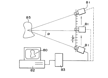
A two-dimensional image 80 of an object 85 to be
three-dimensionally displayed is photographed by using a
TV camera 81. More specifically, one TV camera 81 is
placed at a plurality of positions defined by intervals
CA 02027462 1998-03-13
~, and a plurality of two-dimensional images 85 of the
object 85 corresponding to the respective positions are
photographed. The data of these two-dimensional images 85
is input to a computer 82 by using a digitizer 83 so as to
be stored as image data. In order to input the data of
these two-dimensional images 85 to the computer 82, data
recorded on a video tape may be used, or data of a
photograph or a movie may be used. In addition, the object
85 to be three-dimensionally displayed is not limited to an
existing object but may include computer graphics.
A method of determining a direction Q and a pitch _ of
each diffraction grating will be described below with
reference to Figs. 2 and 3.
Assume that an observer observes a display 15 having a
dot 16 which is manufactured by the method of the present
invention, as shown in Fig. 2. If the incidence angle of
illumination light 91 is ~, the direction of lst-order
diffracted light 92 diffracted by a diffraction grating 18
is ~, and the wavelength of the lst-order diffracted light
92 is A as shown in Fig. 2, a direction Q of the
diffraction grating 18 and a pitch _ (the reciprocal of a
spatial frequency) of the diffraction grating 18 can be
obtained by the following equations. Assume that the
illumination light 91 propagates on the Y-Z plane, and the
diffracted light propagates on the X-Z plane.
CA 02027462 1997-06-18
2027462
tan(n) = sin(a)/sin(~)
d = A/~sin2(0) + sin2(a)
By using the above equations, the direction Q and
the pitch d of the diffraction grating 18 which are used
to diffract the illumination light 91 in an arbitrary
direction can be obtained. That is, if the incidence
angle 0 of the illumination light 91, and the direction
and the wavelength A of the lst-order diffracted light
92 are provided, the direction n and the pitch d of the
diffraction grating 18 can be obtained.
Delineation of a diffraction grating by means of an
electron beam scanning unit will be described below with
reference to Figs. 4 and 5.
The electron beam scanning unit comprises an elect-
ron gun 50, an alignment 52, a blanker 54, a condenser
lens 56, a stigmator 58, a deflector 60, an objective
lens 62, and an X-Y stage 20. An EB resist (dryplate)
14 is placed on the X-Y stage 20. The blanker 54, the
deflector 60, and the X-Y stage 20 are connected to a
computer 66 through a control interface 64. An electron
beam radiated from the electron gun 50 scans the dry-
plate 14 under the control of the computer 66.
Fig. 5 shows the dryplate 14 placed on the X-Y
stage 20. An electron beam 70 emitted from the electron
gun 50 is used to delineate diffraction gratings 18 in
units of dots 16. The diffraction gratings 18 are
sequentially delineated in units of dots by moving the
CA 02027462 1997-06-18
~027462
X-Y stage 20.
A sequence of operations will be described below
with reference to Fig. 6.
In step al, an Nth two-dimensional image of an
object to be three-dimensionally displayed is photo-
graphed by the TV camera, and image data of the two-
dimensional image is read and input to the computer.
Alternatively, image data of computer graphics may be
input to the computer. In addition, after all the
required two-dimensional images of an object to be
three-dimensionally displayed are photographed at a plu-
rality of photographing positions and are input to the
computer, an Nth two-dimensional image may be selected
from the data of the plurality of two-dimensional
images.
In step bl, the two-dimensional image is corrected
in the computer. This is because a two-dimensional
image input to the computer often requires correction
for, e.g., distortion and contrast.
In step cl, a light source position and a view
direction in observation of the display of the present
invention are input to the computer.
In step dl, the X-Y stage is moved to the origin.
In step el, dot data associated with the Nth two-
dimensional image is input from a data file to the
computer. Of the image data of the corrected two-
dimensional image, this dot data is associated with the
CA 02027462 1997-06-18
~2027462
- 10 -
position, color (wavelength)~ and brightness of the
above-mentioned dot, and the direction of the dot with
respect to the stereoscopic object assumed when the two-
dimensional image including the dot is fetched.
Subsequently, in steps fl, gl, and hl, the pitch
and direction of a diffraction grating and the area of
the dot are determined on the basis of these data and
the light source position and the view direction input
in step cl. The pitch and direction of the diffraction
grating are obtained by using the above-mentioned
equations. The area of the dot is set to be propor-
tional to the brightness of a portion of the object
which corresponds to the dot. Note that the order of
steps fl, gl, and hl is not limited to the above order
but may be variously changed.
In step il, the X-Y stage is moved to the position
of the dot to be delineated on the basis of the dot data
input in step el. In step jl, a diffraction grating for
the dot is delineated by using the above-described elec-
tron beam scanning unit. With this series of steps,
delineation of the diffraction grating corresponding to
one dot is completed.
Subsequently, in step kl, the address of the data
file is incremented by one in order to refer to the data
of the next dot. If it is determined in step ~1 that
image data corresponding to this address is present,
the flow returns to step el to input the data of another
CA 02027462 1997-06-18
t.~.O274.~'2
-- 11 --
dot, and steps fl, gl, hl, il, jl, and kl are repeated.
This series of steps is continued until all the image
data corresponding to the dots of the Nth two-
dimensional image are processed. With this processing,
delineation of a diffraction grating pattern based on
the image data of the Nth two-dimensional image is
completed.
If it is determined in step ~1 that delineation of
the Nth two-dimensional image is completed, the flow
advances to step ml to refer to an (N+l)th
two-dimensional image. If it is determined in step nl
that the (N+l)th two-dimensional image is present, the
flow returns to step al, and steps al to ~1 are
executed. With this processing, diffraction grating
patterns corresponding to the (N+l)th two-dimensional
image are formed.
If the loop consisting of steps al to nl is exe-
cuted in this manner and it is determined in step nl
that no further three-dimensional image is present,
delineation of all the diffraction gratings is
completed.
The dryplate having the diffraction grating pat-
terns formed in this manner is used as a master plate
for duplication. Duplication is performed by a well-
known embossing method.
The second embodiment of the present inventionwill be described below with reference to Figs. 7 to 10.
CA 02027462 1997-06-18
2027462
- 12 -
This embodiment is a method of manufacturing dots of
diffraction gratings by interference of two laser beams.
Fig. 7 is a perspective view for explaining a
method of manufacturing a display having diffraction
grating patterns by interference of two laser beams. More
specifically, as shown in Fig. 7, when two laser beams 170a
and 170b are caused to interfere with each other on a
dryplate 114, interference fringes 118 are formed on a dot
116. The cycle of the interference fringes 118 can be
changed by changing the angle at which the two laser beams
170a and 170b interfere with each other. Dots 116 each
consisting of the interference fringes 118 are formed on
the dryplate 114 while an X-Y stage 120 and a rotary (0)
stage 128 are moved in accordance with commands from a
computer. In this case, in order to form three types of
dots 116 representing three colors, i.e., red (R), green
(G), and blue (B), laser beams of three angles are
prepared. In this manner, three color spots of red (R),
green (G), and blue (G) are formed at arbitrary positions
on the dryplate 114 in accordance with comm~n~ from the
computer. The disclosure of aforementioned European Patent
Application No. 0357837 A2 may be referred to in order to
determine the angles of laser beams.
Fig. 8 shows an optical system for forming dots
on a dryplate. Referring to Fig. 8, the optical path of
CA 02027462 1997-06-18
2027462
a laser beam emitted from a laser 122 iS changed by
total reflection mirrors 124 and 126. The laser beam is
then incident on half mirrors 132, 134, and 136 so as to
be divided into four laser beams Bl, B2, B3, and B4. At
this time, the four laser beams Bl, B2, B3, and B4 are
set to have the same intensity. One of the three laser
beams Bl, B2, and B3 is selected by a slit 138 and is
radiated on the dryplate 114 through lenses 140 and 142.
In addition, the laser beam B4 as reference light is
incident on the dryplate 114 through mirrors 144 and
146. In this case, the four laser beams Bl, B2, B3, and
B4 are adjusted to be concentrated at a point. In
addition, the angles at which these four laser beams Bl,
B2, B3, and B4 are incident on the dryplate 114 are set
to values calculated in advance so as to allow dif-
fracted beams from diffraction gratings to respectively
represent red (R), green (G), and blue (B).
The dryplate 114 is placed on the x-Y stage 120.
The X-Y stage 120 is mounted on the 0 stage 128. These
stages (x-y-o stage) can be moved under the control of
the computer. In addition, an exposure or non-exposure
operation using the four laser beams Bl, B2, B3, and B4
is controlled by opening/closing of a shutter 148
arranged in front of the dryplate 114.
A method of manufacturing a display having diffrac-
tion grating patterns according to the second embodiment
will be described below with reference to Fig. 9.
CA 02027462 1997 - 06 -18 2 0 2 7 4 6 2
-- 14 --
In step a2, an Nth two-dimensional image of an
object to be three-dimensionally displayed is photo-
graphed by a TV camera, and image data of the two-
dimensional image is read and input to the computer.
Alternatively, image data of computer graphics may be
input to the computer. In addition, after all the
required two-dimensional images of an object to be
three-dimensionally displayed are photographed at a
plurality of photographing positions and are input to
the computer, an Nth two-dimensional image may be
selected from the data of the plurality of two-
dimensional images.
In step b2, the two-dimensional image is corrected
in the computer. This is because a two-dimensional
image input to the computer often requires correction
for, e.g., distortion and contrast.
In step c2, a light source position and a view
direction in observation of the display of the present
invention are input to the computer.
In step d2, the X-Y stage is moved to the origin.
In step e2, corresponding dot data is input from a data
file to the computer. Of the image data of the cor-
rected two-dimensional image, this dot data is associ-
ated with the position, color, and brightness of the
above-mentioned dot, and the direction of the dot with
respect to the panorama parallax object assumed when the
two-dimensional image including the dot is fetched.
CA 02027462 1997-06-18
2027462
- 15 -
Subsequently, in steps f2, g2 and h2, the pitch
and direction of a diffraction grating and an exposure time
are determined on the basis of these data and the light
source position and the view direction input in step c2.
The direction of the diffraction grating are obtained by
using the above-mentioned equations. When, angle ~ of a
lst-order diffracted light is small, the pitch of the
diffraction gratings depends on only a reproduced light
color. Therefore the pitch corresponding to the color of
the dot is selected from the pitches of the R, G and B.
European Patent Application No. 0357837 A2 may be referred
to in this regard. The exposure time can be set in
accordance with a time during which the shutter of the
exposure unit in Fig. 8 is opened. The exposure time is
set to be proportional to the brightness of a portion of
the object which corresponds to the dot. Note that the
order of steps f2, g2, and h2 is not limited to the above
order but may be variously changed.
In step i2, the X-Y stage and 0-stage (X-Y-0
stage) are moved to the position of the dot to be exposed
on the basis of the dot data input in step e2. In step j2,
exposure of a diffraction grating for the dot is performed
by using the two-beam interference unit shown in Fig. 8.
With this series of steps, formation of the grating
corresponding to one dot is completed.
Subsequently, in step k2, the address of the data
CA 02027462 1997-06-18
2027462
- 16 -
file is incremented by one in order to refer to the data
of the next dot. If it is determined in step ~2 that
image data corresponding to this address is present, the
flow returns to step e2 to input the data of another
dot, and steps f2, g2, h2, i2, j2, and k2 are repeated.
This series of steps is continued until all the image
data corresponding to the dots of the Nth two-
dimensional image are processed. With this processing,
formation of a diffraction grating pattern based on
the image data of the Nth two-dimensional image is
completed.
If it is determined in step ~2 that the formation
of the Nth two-dimensional image is completed, the flow
advances to step m2 to refer to an (N+l)th two-
dimensional image. If it is determined in step n2 that
the (N+l)th two-dimensional image is present, the flow
returns to step a2, and steps a2 to ~2 are executed.
With this processing, diffraction grating patterns cor-
responding to the (N+l)th two-dimensional image are
formed.
If the loop consisting of steps a2 to n2 is
executed in this manner and it is determined in step n2
that no further three-dimensional image is present,
formation of all the diffraction gratings is completed.
The dryplate having the diffraction grating pat-
terns formed in this manner is used as a master plate
for duplication. Duplication is performed by a well
CA 02027462 1997-06-18
2027462
- 17 -
known embossing method.