Language selection

Search

Patent 2027495 Summary

Third-party information liability

Some of the information on this Web page has been provided by external sources. The Government of Canada is not responsible for the accuracy, reliability or currency of the information supplied by external sources. Users wishing to rely upon this information should consult directly with the source of the information. Content provided by external sources is not subject to official languages, privacy and accessibility requirements.

Claims and Abstract availability

Any discrepancies in the text and image of the Claims and Abstract are due to differing posting times. Text of the Claims and Abstract are posted:

  • At the time the application is open to public inspection;
  • At the time of issue of the patent (grant).
(12) Patent: (11) CA 2027495
(54) English Title: PROCEDURE AND APPARATUS FOR AMPLIFICATION OF A BURST SIGNAL
(54) French Title: METHODE ET APPAREIL D'AMPLIFICATION DE SIGNAUX EN SALVE
Status: Deemed expired
Bibliographic Data
(52) Canadian Patent Classification (CPC):
  • 325/101
  • 363/17
(51) International Patent Classification (IPC):
  • H04J 3/06 (2006.01)
  • H03G 3/20 (2006.01)
  • H04B 1/18 (2006.01)
  • H04L 5/14 (2006.01)
(72) Inventors :
  • BRAHMS, MARTIN (Germany)
  • HENNIG, ANDREAS (Germany)
  • TIMMERMANN, ANDREAS (Germany)
(73) Owners :
  • KE KOMMUNIKATIONS ELEKTRONIK GMBH & CO (Germany)
(71) Applicants :
(74) Agent: SMART & BIGGAR
(74) Associate agent:
(45) Issued: 1994-05-24
(22) Filed Date: 1990-10-12
(41) Open to Public Inspection: 1991-04-15
Examination requested: 1991-12-18
Availability of licence: N/A
(25) Language of filing: English

Patent Cooperation Treaty (PCT): No

(30) Application Priority Data:
Application No. Country/Territory Date
P 39 34 384.7 Germany 1989-10-14

Abstracts

English Abstract


ABSTRACT OF THE DISCLOSURE

A controllable amplifier, which has two
symmetrical outputs, at which two output signals mirror-
symmetrical with respect to each other are present, is
used for amplification of a burst signal. To achieve
the largest possible eye opening of the signals to be
fed to a comparator, a predetermined d.c. voltage
difference for the formation of matched signals is
adjusted for both output signals. After this, the
arithmetic mean values of the two matched signals are
formed and are fed to a second comparator. The output
value of the second comparator is fed to an integrator,
to which a reference voltage is also fed. In case of a
deviation of the mean values of the two matched signals
from each other, the amplifier is adjusted in a
compensating direction by the integrator.


Claims

Note: Claims are shown in the official language in which they were submitted.


THE EMBODIMENTS OF THE INVENTION IN WHICH AN EXCLUSIVE
PROPERTY OR PRIVILEGE IS CLAIMED ARE DEFINED AS FOLLOWS:

1. A procedure for amplification of a burst signal,
comprising the steps of:
feeding the burst signal to a controllable amplifier
with two symmetrical outputs, at which two output signals mirror-
symmetrical with respect to each other are present;
adjusting the two output signals so that a
predetermined d.c. voltage difference is provided for the
formation of matched signals;
forming the arithmetic mean values of the two matched
signals and feeding the mean value to a comparator;
feeding the output value of the comparator to an
integrator, to which a reference voltage is also supplied; and
adjusting the amplifier in a compensating direction by
means of an output from the integrator in the event of a
deviation between the mean values of the two matched signals.

2. A procedure according to claim 1, wherein only the
bursts are used for the formation of the mean values of the two
matched signals.

3. A circuit arrangement for amplification of a burst
signal, comprising:
a controlled amplifier having an input for receiving
the burst signal and two symmetrical outputs for providing two
mirror-symmetrical output signals;
a CR network having two inputs connected to the two
symmetrical outputs and having two outputs;


a lowpass filter having a pair of inputs connected to
the outputs of the CR network and providing two outputs;
a comparator having two inputs connected to the two
outputs of the lowpass filter, said comparator also having an
output: and
an integrator having an input connected to receive the
output of the comparator and a second input for receiving a
reference voltage and having an output connected to a control
input of the amplifier.

4. A circuit arrangement as described in claim 3, wherein
the lowpass filter comprises RC elements.


Description

Note: Descriptions are shown in the official language in which they were submitted.


2027~9~

PROCEDURE AND APPARATUS FOR AMPLIFICATION OF A
BURST SIGNAL


BACKGROUND OF THE INVENTION
Field of the Invention
The present invention relates to a procedure and
apparatus for amplification of a burst signal, as is
used in the bi-directional transmission of
communications signals in a time-division multiplex
(TDM) procedure.


Description of the Prior Art


In a TDM system, the signals in both transmission
directions are conducted over the same signal path,
which can be formed by metallic conductors or optical
waveguides. Between the individual bursts transmitted
in one direction, in which a continuous data stream is
contained in a form compressed with respect to time,
there are relatively large time differences, which are
intended for transmission of bursts in the opposite
direction. What is present in burst operation is
therefore not a continuous, but a strongly
discontinuous data signal transmission. This type of
signal transmission requires a satisfactory further

2027~95

processing of the signals, the bursts, in regenerators
and receivers which use comparators.


SUMMARY OF THE INVENTION


The invention is based on the task of providing a
procedure by means of which, in the amplification of
burst signals, the largest possible eye opening can be
produced in a simple manner.
According to the invention, this task is solved by
the fact


- that the burst signal is fed to a
controllable amplifier with two symmetrical
outputs, at which two outputs signals mirror-
symmetrical with respect to each other are
present,


- that a predetermined d.c. voltage difference
for the formation of matched signals is
adjusted for the two output signals,


- that the arithmetic mean values of the two
matched signals are formed and are fed to a
-comparator,


- 2 -

.

2~2749~

- that the output value of the comparator is
fed to an integrator, to which a reference
voltage is also supplied, and


- that, in the case of deviation of the mean
values of the two matched signals from each
other, the amplifier is adjusted in the
compensating direction by means of the
integrator.


In this procedure, a defined d.c. voltage
difference is initially established between the two
mirror-symmetrical output signals of the amplifier, for
example, by means of a simple RC network. The
amplification of the signals is controlled in such a
way that the arithmetic mean values of the signals
matched by the RC network are located at the same
potential. This results in a maximum eye opening of
the bursts, so that a comparator connected in series
can make the best possible decision. A simple
comparator can therefore be used. The formation of the
arithmetic mean values of the two matched signals is
also very simple, for example, with the use of lowpass
filters, which can be simple, RC elements. By means of


-- 3 --

.~
'~3

-" 2027~9~

the comparator and the integrator connected in series,
the amplifier is continuously adjusted in a
compensating direction without major effort, so that
bursts with a maximum eye opening are continuously fed
to the amplitude decider. Despite the discontinuous
operation, a satisfactory amplification or regeneration
of the bursts signals is thus ensured in a simple
manner.
The procedure according to the invention is
explained by means of examples below, with reference to
the drawings.


DESCRIPTION OF THE DRAWINGS


Figure 1 is a schematic representation of a
circuit arrangement for execution of the procedure
according to the invention.
Figure 2 is an excerpt of a signal to be
processed.
Figure 3 shows the siqnals after the amplifier, in
enlarged representation.


~,


-- 4


.
' .

` 2027~9S

DETAILED DESCRIPTION OF THE PREFERRED EMBODIMENT


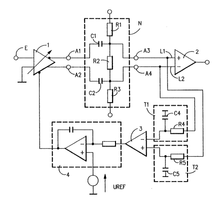
Figure 1 shows a circuit arrangement for
amplification of a burst signal in a very simple
embodiment, in which only the parts required for an
understanding of the invention have been shown.
By means of an input E there is fed to a
controllable amplifier 1 a burst signal, an excerpt of
which is shown, in principle in Figure 2. A burst
signal of this type is used in communication
transmission, particularly in the TDM systems, in
which, in the intervals between two bursts of one
transmission direction, the bursts of the other
direction are transmitted via the same signal path.
The intervals between the bursts are very long in
comparison with the time length of the bursts, so that
a strongly discontinuous data signal is produced
overall. The amplified burst signal is fed to a
comparator 2.
The controllable amplifier 1 has a control input R
and two symmetrical or complementary outputs A1 and A2,
at which there are provided two mirror-symmetrical
signals, which are inverted in terms of a.c. voltage.
A defined d.c. voltage difference for the two output
~ signals is formed by means of a RC network N, enclosed


!

;~ ~

t

2~27495

by broken lines in the Figure 1. The RC network N
includes capacitors Cl and C2 and the resistors Rl, R2
and R3. In this way, the arithmetic mean values or
zero lines of the two output signals are related to
each other in a specific manner. The zero lines of the
two output signals of the amplifier 1 are shown by dash-
dotted lines in Figure 3. The potential difference
between them is designated as U. At the outputs A3
and A4 of the RC network N there are thus present
signals which, by specification of their zero lines,
have a preset position or a preset distance from each
other, so that they can be superposed. The signals
present at A3 and A4 will be referred to as "matched
signals" below.
The matched signals are conducted separately over
the lines Ll and L2 and are fed to an amplitude
comparator 2. They are also tapped off separately, and
are fed to lowpass filters T1 and T2 to form their
arithmetic mean values. With the circuit shown in
Figure 1, only the bursts of the signals are used for

the formation of the mean values. In the present case,
RC elements with the resistors R4 and R5 and the
capacitors C4 and C5 are used as the lowpass filters Tl
and T2. However, LR elements or active integrators can
also be used.


202749~
The mean values of the two matched signals are fed
to a comparator 3, which compares these mean values or
their position with their respect to each other. To
the comparator 3 there is connected an integrator 4
with an input, to which a reference voltage UREF is fed
via another input. The output of the integrator 4 is
connected to the control input R of the amplifier 1.
In the case of a deviation of the mean values of the
matched signals from each other, the amplifier 1 is
adjusted in a compensating direction by means of the
integrator 4. This means that, in order to achieve the
largest possible eye opening of the bursts reaching the
comparator 2, the mean values of the two matched
signals are located on the line M drawn in as a dashed
line in Figure 3.
To form the mean values of the two matched signals
- as described - only the bursts themselves are used in
a preferred embodiment. The formation of the mean
values thus becomes independent of the time length of
the bursts and the burst intervals. If the whole burst
signal is used for formation of the mean values, then
it is necessary to also take into consideration at
least the peak value (amplitude) of the bursts and the
burst/interval ratio.


'

Representative Drawing
A single figure which represents the drawing illustrating the invention.
Administrative Status

For a clearer understanding of the status of the application/patent presented on this page, the site Disclaimer , as well as the definitions for Patent , Administrative Status , Maintenance Fee  and Payment History  should be consulted.

Administrative Status

Title Date
Forecasted Issue Date 1994-05-24
(22) Filed 1990-10-12
(41) Open to Public Inspection 1991-04-15
Examination Requested 1991-12-18
(45) Issued 1994-05-24
Deemed Expired 2001-10-12

Abandonment History

There is no abandonment history.

Payment History

Fee Type Anniversary Year Due Date Amount Paid Paid Date
Application Fee $0.00 1990-10-12
Registration of a document - section 124 $0.00 1991-03-13
Maintenance Fee - Application - New Act 2 1992-10-12 $100.00 1992-09-17
Maintenance Fee - Application - New Act 3 1993-10-12 $100.00 1993-09-08
Maintenance Fee - Patent - New Act 4 1994-10-12 $100.00 1994-09-14
Maintenance Fee - Patent - New Act 5 1995-10-12 $150.00 1995-09-12
Maintenance Fee - Patent - New Act 6 1996-10-14 $150.00 1996-09-12
Maintenance Fee - Patent - New Act 7 1997-10-14 $150.00 1997-09-24
Maintenance Fee - Patent - New Act 8 1998-10-13 $150.00 1998-09-24
Maintenance Fee - Patent - New Act 9 1999-10-12 $150.00 1999-09-13
Owners on Record

Note: Records showing the ownership history in alphabetical order.

Current Owners on Record
KE KOMMUNIKATIONS ELEKTRONIK GMBH & CO
Past Owners on Record
BRAHMS, MARTIN
HENNIG, ANDREAS
TIMMERMANN, ANDREAS
Past Owners that do not appear in the "Owners on Record" listing will appear in other documentation within the application.
Documents

To view selected files, please enter reCAPTCHA code :


To view images, click a link in the Document Description column. To download the documents, select one or more checkboxes in the first column and then click the "Download Selected in PDF format (Zip Archive)" or the "Download Selected as Single PDF" button.

List of published and non-published patent-specific documents on the CPD .

If you have any difficulty accessing content, you can call the Client Service Centre at 1-866-997-1936 or send them an e-mail at CIPO Client Service Centre.


Document
Description 
Date
(yyyy-mm-dd) 
Number of pages   Size of Image (KB) 
Cover Page 1994-07-09 1 24
Abstract 1994-07-09 1 21
Drawings 1994-07-09 1 17
Claims 1994-07-09 2 51
Description 1994-07-09 7 185
Representative Drawing 1999-07-19 1 11
Correspondence 2003-11-24 1 19
Fees 2003-11-07 3 147
Office Letter 1992-03-18 1 48
PCT Correspondence 1994-02-28 1 17
Prosecution Correspondence 1991-05-17 1 36
Prosecution Correspondence 1992-08-24 1 36
Prosecution Correspondence 1991-12-18 1 28
Fees 1995-09-12 1 37
Fees 1996-09-12 1 44
Fees 1993-09-08 1 29
Fees 1994-09-14 1 39
Fees 1992-09-17 1 22