Note: Descriptions are shown in the official language in which they were submitted.
f'l ~ h/ ~f J 3 ~
PPF 2 003
INTRIN~ICALLY ~AFE BARRIER DEVICE
13ackaround of th~ Invention
This application pertains to the art of
intrinsically saEe or protection barrier devices, and more
particular to provision of such barrier devices which
function in a non-destructive manner.
The application is particularly applicable to
provision of electric power to devices disposed within
hazardous areas, and will be descrlbed wi-th particular
reference thereto. It will be appreciated, however, that
the invention has broader applicatioll, such as in any
application in which a device ls to be isolated against
over voltages, over current, reverse polarity connectiolls,
and the like.
Intrinsic safety is generally considered the safest
method of supplying electricity to equipment disposed in
hazardous areas. Such hazardous areas include highly
combustible areas, and include such applications as
monitoring devices disposed in fuel storage areas. Such
intrinslc barrler devices provide a reliable, less
expensive, and more desirable approach to providing power
to systems in such areas then are found in the
alternatives. Alternatives include such means as encasing
an entire system within an explosion proof barrier. Such
barriers are obviously bulky, high in weight, and extremely
expensive to construct, and maintain.
Presently, several intrinsically safe barrier
devices are available. These include "zener barrier
modules" which typically incl-lde zener diodes, a resistor,
and a fuse. The zener d:iode functions to clamp over
voltages. In the event of excessive current or over
voltage conditions, the fuse will blow. The blowing oE a
use in such a barrier module typically requires
-- 2
replacement of the entire subsystem, given that a
substantial possibility exists that the zener diode, or
diodes, were damaged by -the clamping action. Such
replacement is generally expensive. In addition, there is
generally no means to readily discern whether, in fact, a
fuse in such a zener barrier module has been blown.
Other attempts have been made to fabricate
alternative secure intrinsically barrier devices, typically
with systems utilizing a plurali-ty of electronic
components. Rs electronic components themselves require
power for operation, other disadvantages arise. In
particular, a separate power supply must be provided to the
device, or the devlce is sub~ect to voltage drops between
its input and output. Such voltage drops are generally
unacceptable, especially in areas where the voltage
supplied -to the hazardous area must be maintained in close
tolerance to generated voltage levels.
The present invention contemplates a new and
improved intrinsically safe barrier device which overcomes
all of the above-referred problems, and others, and
provides a reusable barrier device which is reliable and
economical.
In accordance with the present invention, there is
provided an protection barrier device which includes first
and second input terminals adapted for connection of the
device with an associated direct current voltage source.
first series path is providad between the first input
terminal and first output terminal. Similarly, a second
series path is provided between the second input terminal
and second output terminal. A current sensing means is
provided to sensing current levels in at least one of the
first and second series paths. Means is provided for
generating a signal representative of an event in whlch
' 'SJ ~ ~ i
excessive currents, defined to selected standardsl causing
a triggering of a crowbar circuit disposed between the
first and second series paths. This crowbar circui-t, in
turn, provides a low resistance current path between the
series paths. Current flowing through this crowbar circuit
path, in turn, triggers a switching means which functions
to impede current flow tnrough at least one of the first
and second series paths.
In accordance with a more limited aspect oE the
present invention, means is also provided for protecting
the hazardous area from receiving signiEicant voltage when
the first and second input terminals are misswired to
reversed potentials.
In conjunction with a yet more limited aspect of the
subject invention, a thermis~or is disposed in at least one
of the first and second series paths, which thermistor
functions to minimize current in the event the switchiny
means is bypassed, or fails.
In accordance with another aspect of the present
tnvention, a method of intr~nsic protection for operation
of the afore-mentioned means is disclosed.
An advantage of the present invention is the
provision of a system which reacts quickly to over current
conditions, over voltage conditions, reverse polarity
conditions, and short circuit conditions.
Another advantage of the present invention is the
provision of a system having a readily discernable visual
indicator of when a ault has been detected, and
compensated for.
Yet another advantage of the present invention is
the provision of a system for intrinsically safe voltage
protection which maintains a minimum vol-tage drop between
input and outputs thereof.
- 4 - ~ 31
Further advantages will be obvious to one of
ordinary skill in the art upon a reading and understanding
of the subject invention.
Br~ef Dss~ription of the Dr~winqs
The invention may take physical form in certain
partsl and arrangements of parts, preferred and alternate
embodiments of which will be described in detail in this
specification, and illustrated in the accompanying drawings
which form a part hereof, and wherein:
FIGURE 1 illustrates, in schematic form, an
intrinsically sae barrier circuitry of the subject
invention; and
FIGURE 2 illustrates, in block diagram form, a
protection barrier module including the circuitry of
FIGURE 1.
Detalled Descrlption of tha
Pre~erred ~na Altern~to Embod~ents
Referring now to the drawings wherein the showings
are for the purposes of illustrating the preferred and
alternate embodiments of the invention only, and not for
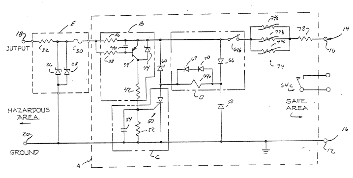
the purposes of limiting the same, FIGURE 1 illustrates an
protection barrier circuit A which includes a current
detection system B, a quick protection system C, and a
long-term protection D~ Also illustrated is a zener
barrier module E, such as is typ~cally utilized in the
prior art.
The circuitry of FIGVRE 1 includes first and second
input terminals or means 10 and 12 respectively. These
terminals form first and second current series paths 14 and
16, with first and second output terminals 18 and 20,
respectively. In the pref~rred embodiment, the circuitry
of FIGURE 1, in addition to all circuitry disposed prior to
-- 5
input terminals 10 and 12 is found in a "safe area,"
defined as an area substantially devoid of combustible
fuels, or the like. Outpu-t terminals 18 and 20 form and
electrical connection to systems disposed in a hazardous
area.
The zener barrier module E forms the sole protection
in a typical protection barrier device. Included therein
is a zener diode which functions to shunt first and second
series current paths 14 and 16 in the event of over voltage
or over current. Illustrated is first and second parallely
mounted zener diodes 26 and 28 so arranged to divide
current flow therebetween. It will be appreciated by one
o~ ordinary skill in the art that the zener diode
facilitates low resistance conduction once a threshold
voltage, determined by diode characteristics, has been
achieved. Over current conditions, such as would be
introduced after triggeriny of the zener diodes, causing
blowing of a fuse 30. A small voltage drop is introduced
into the first series current path 14 by resistor 32.
As note above, though functional, upon action of
zenar barrier module Pmploying circuitry such as that
illustrated, no readily available visual indicator of a
tripped condition is available. In addition, it is
desirable to replace the entire unit after a fuse has been
blown in the ev~nt that undetectable damage occurred to the
zener diodes. The protection barrier circuit A may serve
dual capacit~es. It may serve as a primary protection
circuit for zener barrier modules such as that illustrated
by E.
The current detection system B is sensitlve to
current flow through first series current path 14. A base
of transistor 34 i5 energized in accordance with a voltage
difference dictated by relative values of resistors 36 and
-- 6
38, and capacitor 40, as will be appreciated by one of
ordinary skill in the art. Upon achieving current in
current path 14 of a selected level as dictated by this
combination, the transistor 34 is caused to conduct through
its emitter-collector junction, providing current flow
through biasing resistor 42 into the quick protection
system C. Zener diode 44 serves to prevent the emitter-
collector ~unctlon from damage due to transient voltages.
The quick protection system C includes a silicon
controlled rectifier ("SCR"), the gate oE which is
interconnected with an output of current detection system
emanating from resistor ~2. The gate is also connected to
a parallel resistor-capacitor t"R/C") network form from
resistor 52 and capacitor 54. The anode oE SCR 50 is
electrically connected to first series current path 14 to
allow in flow of conventional current thereinto in a
fashion which will be described further below. The cathode
of SCR 50 is electrically connected to second series
current path 16. It will be appreciated that upon
triggering of the SCR 50 by application of voltage to its
gate lead, a low resistance current path is therefore
provided between first series current path 14 and second
series current path 16, provided that conventional current
flow is in that same direction. This shunting effect is
commonly referred to as a "crowbar," thereby providing a
common designation of the quick protection system C as a
crowbar circuit.
As will be inferred from the above-description, the
over current or over voltage problems compensated for by
the combination of the current detection system E and quick
protection system c are unaccounted for in a reverse
polar~ty situation. That is, ln the event conventional
current flow was to occur from second input terminal to
-- 7 --
first input terminal lo, the triggering would not QccUr .
This situation is independently accounted for by diodes 58
and 60, which are mounted, in series, to form a low
resistance path for conventional current flow from the
second series current path 16 to the first series current
path 14. This combination provides quick reverse polarity
protection for the intrinsically safe barrier circuit A.
Particular interconnections between a cathode of diode 58
and series connected anode of diode 60 will become apparent
with the description of long-term protection system D,
which follows.
The long-term protection system D includes a current
sensitive switching circuit or means 6~ which, in the
illustrat~d embodiment, employs a coil portion 64a and a
normally closed contact portion 64b. It will be
appreciated that current flow of a sufficient magnitude
through coil portion 64a results in a tripping, or opening
of coil portion 64b thereby causing an effective break in
the first series current path 14. Such current may be
introduced through coil 64a through diode 66 and SCR 50
upon triggering of the quick protection system C, as
described above. Additionally, current flow through coil
portion coil portion 64a is induced by reverse polarity
connection of input contracts 10 and 12 given that the
coils 64a is disposed in current series between an anode of
diode 58 and cathode of diode 60. It will therefore be
noted that tripping of the switching circuit 64 is
accomplished in either condltion. In the illustrated
embodiment, diodes 68 and 70 are also provided to protect
the coll portion 64a from transient~ and back EMF, as will
be appreciated from one of ordinary skill in the art.
It is often desirable that a remote signal be
provided evidencing a tripping of a barrier d~vice. Such a
signal is suitably provided by an additional pair of
contacts 64c on the switching circuit 64. Such contacts
add no additional voltage drop across the device, and may
be installed as normally open or normally closed as a
particular installation may warrant.
In the illustrated embodiment, the switching circuit
64 is comprised of a current operated circuit breaker or
relay. As will be noted with FIGURE 2, reset switch is
also utilized which additionally functions to provide a
visual indicator o a tripping thereof. Utilization of a
contact device is advantageous given that essentially 110
voltage drop Is experienced across the contacts. lt will
also be appreciated that other suitable switchin~ means,
such as transistors and especially field effects
transistors may be suitable utilized in place of the
illustrated breaker. With present technology, some voltage
drop will be experience with most semi-conductor elements
used for such switching purposes. It is envisioned that
certain application may not be voltage sensitive allowing
for the use of such elements or further advances in
fabrication wlll minimize losses to within acceptable
levels. When such semi-conductor elements are utilized as
the switching means, an additional signaling device, such
as a light-em~tting diode, or the like, are advantageously
used to replace the visual indicator provided by the
circuit breaker in the illustrated embodiment.
A thermistor network 74 is also advantageously
applied in the circuit, and is illustrated in first series
current path 14. It will be appreciated that such
thermistors maintain a resistance proportional to
temperature. A suitable thermistor is defined as having a
normal resistance in around 3 n, and a high temperature
resistance of over 20 n in overheated conditions induced by
~ ~ s~ ~J ~
- 9 -
excessive current flow therethrough. The thermistor
network 74 is provided as a ~ail-safe mechanism in the
event that the switching circuit 64 is forcibly shorted,
notwithstanding an otherwise open condition, or in the
event the element fails, in its entirety. In the
illustrated embodiment, three parallely mounted thermistors
74a, 74b, 74c are utilized to minimize current handling
requirements of any o~ the thermistors, individually.
Finally, a small input resistor 78 is provided to provide
nominal isolation of the protection barrier circuit ~ from
the actual power generating system. A suitable resistance
~alue of lOn provides nom~nal voltage losses in t~ptcal
ranges (50m~) passed by the barrier device, but clissipates
considerable power in excess current situations.
It will be seen from the figure that the illustrated
components provide ~or quick protection for over voltage or
over current condition by interaction of the current
detection system B and the quick protection system C.
Reverse bias protection is afforded by interaction of the
diodes 58 and 60. Reverse polarity connections, or
tripping of the quick protection ~ircuit C result in
opening first series current path 14 via long-term
protection system D. A visual indicator is provided in the
event the long-term protection system D has been utilized.
The system is resettable after tripping to eliminate the
necessity of component replacement. Finally, thermistor
network 74 provides a fail-safe mechanism in the event of
bi-passing the protection system, or failure of selected
components thereof. The system is envisioned to be usable
in and of itself, or as a protection system to prevent
destru~tion o~ zener barrier modu~es, such as zener barrier
module E.
~J~ ~J.~ ~
-- 10 --
Turning briefly to FIGURE 2, illustrated is the
protection barrier circuit A and the zener barrier module E
of FIGURE 1 secured within a housing 82, to facilitate
removal or replacement in mounting brackets such as are
commonly used in the field. It will be apparent from the
figure that no additional power supply is necessary to
accomplish the functions of the subject system. Also
illustrated is a reset button or means ~4 which interacts
with the contacts ~4a ~FIGURE 1) for resetting of the
switching circuit, and also provides a visual indlcator of
when the system lies in the a tripplng condition. In the
event that non-mechanical switching means is implemellted,
the indicator 8~ is suitably replaced with a visual
indicator such as a light emitting dlode, or like.
The invention has been described with reference to a
preferred embodiment. ~bviously, modifications and
alterations will occur to others UpOIl a reading and
understanding of this specif~cation. It is intended to
include all such modifications and alterations insofar as
they come within the scope of the appended claims or the
equivalents thereof.