Note: Descriptions are shown in the official language in which they were submitted.
3 I / ~ ~
COMBINED SYNCHRONOUS AND
ASYNCHRONOUS MEMORY CONTROLLER
The invention relates to memory controllers utilized
in computer ~ystems, and more particularly, to computer
systems which allow multiple sources to access a given
block or portion of memory~
Personal computex systems are getting more and more
powerful at a very rapid rate. One rea~on for ~his
increase in power is the development and availability of
more powexful microprocessor~, which form the basi~ of the
personal computer~. New mi~roprocessor desi~ns are being
developed and the clock rates of the exi~ting
microprocessors are b~ing increased so that more and moxe
pex~ormance is available.
With ~he development of 32 bit micxopxoce~sors, the
main m~mory was Reparated from the physi~al ~lot~ provided
for interchangeable boards which were generally~only ~ or
16 ~itfi wide. By separating ~he main ~emory~ arr~y it
2Q became po~ le to m~ke ~he memory array 32 bi~ wide and
to run at siynificantly higher ~peeds then wha~: o~h~rwise
would have been po8~ible over ~e ~u~ co~ecting the
~lots. ~owever, to utilize thi~ memory arxa~ a ~emo~y
con~roller was reguired whi~h~could handle ~y~le~omin~
~ ,' '. ', : ', ''', , ' . '~
2 : !
from the processor and cycles whi~h were generated over
the interchangeable circui~ board bus. To this end
various types of memory controllers were designed for
various systems. For instance, for systems according ~o
~he ~industry ~tandard architectur~ (ISA) based on ~he
International Business Machines Corporation (IBM) PC/AT,
6ynchronous memory controllers were utiliæed based on the
clock provided to the microprocessor. For systems
according to the Micro Channel Architecture ~MCA)
developed by IBM asynchronous memory controllers were
de~eloped because this bus definition was an asynchronous
design, in deference to the synchronous desi~n of the ISA.
One problem with synchronous controllers is that with
each change in microprocessor, either architecture or
speed, the memory controller must be redesigned. Thi~
leads to great complications in each design. While ~n
~synchronous de~ign can be developed, as in the MC~, ~hese
designs are not necessarily be optimized for use with a
. different processor and there~ore there would be
performance degradation as compared to the ultimate limits
possi~le based on given memory devices. Therefore even an
asynchronous design has to be revi~ed with each new
~icroprocessor. Thus system designers were left with ~he
choice of having to redesign the ~emory controller each
time a new processor was utiliz~d, incorporating both
proce~sor related functions and bu~ related functions, or
~o use an asynchronous design with inherent trade offs in
~y~tem pexformance.
The present invention is a memory con~roller which
performs in synchronous mode while operating with ~he
microprocessor of th~ computer ~ys~em and in a~ynchronous
mode when opera~ing with a bus controller locat~d on the
interchangeable circuit board bus or using ~he timing of
~he bu~ In the preferred embodim~nt the i~terchang~ble
circuit board bus is ~he ~t~nded i~du~try standard
~rchitecture (EISA~ bus. The EISA bu~ ~llow6 multipl~
-3- ,
masters to control the bus and thus the memory controller
provides the interface for the bus masters to access the
main m~mory array. The use of the synchronous portion of
the memory controller allows the microprocessor
S performance to be optimized for ~ach microprocessor with
~ini.mal interaction with the EISA bus timings. U~e of the
asynchronous portion allows the portion of the memory
controller relating to the EISA bus to remain constant
during processor changes, thus simplifying the overall
design,task while changing the microprocessor utili~ed in
th~ personal computer.
A better undexstanding of the present invention can
be obtained when the following detailed description of the
preferred embodiment is considered in conjunction with the
following drawings, in which:
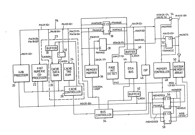
Figure 1 is a block diagram of a personal computer
incorporating the present invention;
Figure 2 is a timing diagram with the synchronous
portion of the memory controller cooperating with ~he
microprocessor;
Figure 3 is a timing diagram of the asynchronous
portion of the memory controller cooperating with the EISA
bus;
Figure 4 is a state machine for use in the
synchronous portion of the memory controller; and
Figures 5-7 are detailed schematics of portions of
the memory controller according to the present invention.
Referring now generally ~o the Figures, the letter C
generally represents a computer system according to the
present invention. A computer system C includ~s a
proces~or 20, preferably the i486 or 80486 micro~rocessor
manu~a~tured by Intel Corporation ~Intel). Information on
the i486 microprocessor is provided in ~he data book
published by In~l and having a date of April 1989.
Cooperating wi~h th~ processor 20 is an op~ional ~umeric
- ,
- . , ~ . . .
- . . , . . ~ . . . .
.
-4~
coprocessor 22, preferably ~he Weitek ~167, which is
designed to coopera~e with the i486. The computer system
c also includes an external cache memory ~y~tem 23 for use
with the processor 20. The addresses provided by the
processor 20 are coupled to form the-processor address bus
PA.~ These address lines PA are connected to the numeric
coprocessor 22 and to the various portions forming the
cache ~ystem 23. The cache tag random access memory (RAM)
24 is used to determine when addresses being requested by
the proce~sor 20 have valid data ~tored in the cache data
~AM 26. Thus the cache tag RAM 24 monitors the processor
address bus PA and provides comparison outputs to a cache
controller 28, which determines when a match is present
based on the comparison values. The cache controller 2~
provides the output ~ignals to a bu~fer 30 which buffers
the processor addresses to the cache data RAM 26. The
cache contxoller 28 also controls a programmable array
logic device (PAL) 32 which performs the n~cessary logical
operations to cooperate with the processor 20 in
developing the lower address lines tG access the cache
data RAM 26. The cache controller 28 intrrfaces with the
processor 20 and the ~umeric coprocessor 22 to use certain
control lines developed by ~e processor 20 and the
numeric coprocessor 22 in its operations.
The cache controller 28 is i~terfaced with a bus
controller 34 which contxols operation of the computer
system C to allow data and addresse~ to be txansferr~d
from the processor portion o ~he computer ~ystem C ~o the
remaining portion~ The bus controller preferably
includes the 82358 E~SA bu~ controller made by Intel. The
bus controller 34 cooperates wi~h ~he a memory mapper 36
which analyzes the processor address bus PA to determine
if ~he memory addresses are located in a ~y~tem memory
arrsy 50 in the co~pu~er ~ystem C, i~ ~he parti~ular
memory location i5 write protected and to develop eertain
addre~e~ to be us~d by the ~y~tem memory array 50. The
bus controller 34 provides ~he proper signals to pass
-5- ;,,J ~ ~J .. ~
address values from the processor address bus PA to a host
address bus ~A. A bidixectional latch 38 is located
between the two address buses HA and PA and receives the
/~APAOE, /PAHAOE, PAHALl~ and HAPALE signal to p~ovide the
output enable and latch enable signâls used by the latch
38.- The bus controller 34 also develops the proper
contxol sign~ls to be used with the bidir~ctional latches
and 42 which respectively provide the address
information and data information to and from the extended
industry architecture (EISA) bus provided for
interchangeable circuit boards. The EISA bus 44 is
developed according to the EISA specification, Revision
3.1. This specification is attached as Appendix 1 to
fully explain the requirements and timings o~ an EISA
system and may be referred to for additional information.
Familiarity with the document is presumed in this
description. The bus controller 34 also cooperates with
the integrated system peripheral (ISP) 46. The integrated
system peripheral 46 handles the direct memory access
~DMA), refresh, interrupt and bus arbitr~tion functions
for a computer system built accordiny to the EISA
specification. The ISP 46 arbitrates whether the
proc~ssor 20, the DMA controller, the refresh controller
or a bus mastar located on the EISA bus ~4 is in control
of the EISA bus ~4, the host bus and the computer system
C. Control rotates based on a priority schedule so that
the devices will gain control of the bus for 60me period
of time.
The bus co~troller 34 cooperate~ wi~h a memory
controller 48 which controls the operation of various
latches and buffer~ and ~he memory d~vices in the system
~emory array ~0. The memo~y controller 48 produces~ a
~ignal ref~rred to as HAM~CLE which i~ the l~tch.enable
signal provided to a latch 52 which tran6fer~ portion~ of
35 the ~ddre6ses provided on ~he host bus HA to the system
memory array 50. Addi~ionally, the ~nemory con~:roller ~8
produces 6iqnal6 referred to as /MUX~S and ~suxcAs which,
- - : . -
- : ~ - , .
. - , . . .
.
. , . . . ,. . .
respecti~ely, enable a buff~r arr~y 54 connected between
the host address ~us HA and the memory addresses provided
by the memory mapper 36 and the system memory array 50 and
~he output of the latch 52 so that row and column
addresses axe properly provided to the memory devices in
the system memory array 50. The memory controller 48 also
provides the /HDMDOE, MDHDLE, /MDHDOEA, and /MDHDOEB and
the bus controller 34 provides the PAHALE signal, which
are supplied to two bidirectional latches 56 and 58 to
transfer data between ~he host ~ata bus HD, whlch is
connected to ~he processor 20, the cache data RAM 26 and
coupled to the EISA bus 44 and the sys~em memory array 50.
Two latches 56 and 58 are utilized in the preferred
embodiment because the system memory array 50 is
preferably 64 bits wide and because the ho~t data bus HD
is preferably 32 bits wide, two buffer sets are utilized.
The memory controller 48 has two portions, an
asynchronous portion for use for controlling accesses by
the ISP 46 or from bus masters located on the EISA bus 44
and a 6ynchronous portion for use for accesses from the
processor 20. Operation of the memory controller 48 and
more details on its construction will be provided.
Figure 2 is a timing diagram of various cycles from
the processor 20 to th~ system memory array 50. A state
machine is utilized by the memory controller 48 and the
stAte of this machine for each given clock cycle is
indicated in the figure. More description of the state
machine will be provided.
The basic clocking signal of the computer system C is
~he CLK1 ~i~nal, the clocking signal applied to the
proces~or 20. In the preferred embodiment ~his is a 25
M~z signal for use with ~he 25 MHz version o the
processcr 20. At time 100, the rising edge o~ the CLKl
signal, the /P~DS ~ignal goes low, which is an indication
by the processor 20 that address information i~ available
for cycle 1. This address information i~ available on the
proces~or address-bus PA as shown. At time 102, ~he ~ext
- . . ;. , ,
rising edge of the CLKl signal, the /HADS signal goes low
to indicate to the bus contr~ller 34 that a valid address
cycle is being performed. Also at this time the /SMEMGO
signal goes low to indicate that a s~stem memory cycle is
S commencing. This signal is used by the memory controller
48 to commence its operations. Also at time 102 the
addresses present on the processor address bus PA and
mapped by the memory mapper 36 are presen~ed to the host
address bus HA through the buffex/latch 38 and a latch 39
from the memory mapper 36, based on the control signals
developed by the bus controller 34. These address signals
on the host address bus are then passed through the latch
52 and the buffer 54 to the memory address bus ~A for
presentation to ~he memory devices.
At ti~e 104, the next rising edge of the CLKl
signal, the /aADS signal goes high and the /SMEMGO sisnal
goes high. At time 106, the next rising edge of the CLKl
signal, the /RAS or row address strobe signal goes low to
indicate to the memory devices that a valid row address is
present. At time 108, the ne~t rising edge of the CLK1
signal, the /MUXCAS signal goes low so that the addresses
for the column in the ~emory devices are presented to the
memory devices. The /MUXRAS ~ignal applied to the buffer
54 is not shown in the timing diagrams for clarity because
it is ~imply ~he inverse of the /MUXCAS ~ignal. Thus when
the /MUXCAS 6ignal is low column addresses are being
provided and when it i~ high row addresses are being
provided to the memory address bus MA.
At time 110, the n~xt risins edge of ~he CLKl ~ignal
the /CAS or column 8ddress 6trobe ~ignal goes low to
indicate to the memory devices that a valid column ~ddress
i6 pre8ent ~nd in ~hi6 case data ~hould be r~ad ~rom the
~emori~6 because the ~MWE ~lgnal i~ high. The m~mory data
begin~ appearing on t~e memory dat~ bus ~hortly
$herea~ter. ~t time 112, the next rising edg~ of the CLK1
signal, th~ data which iæ appearing on ~he ~emory data bus
and the first doubl~ word i~ prese~t~d to the ho~t da a
.. .. . . ............ . . ... . . . . . .
. , , . . . , ~.... :,. .
bus HD. It is noted that the memory system 50 is
pre~erably organized of 80 nsec page mode memory devices
and i~ 64 bits wide so that when an address is presented
to the system memory array 50 two double words are
developed at one time, thu~ allowing selection of the
appropriate buffer/latch 56 or 58 depending upon the
desired double word. Thus at time 112 the proper latch 56
or 58 is enabled to present the first double w~rd to the
host data bus E~.
At time 114, the next rising edge of the CLKl signal,
the MDHDLE signal goes high, thus latching in the values
on the memory data bus into the latches 56 and 58. Thls
transition affects the latching because the latches 56 and
58 have inverted gating inputs. The system C can now
~tart accessing the second guadruple word to be accessed
in the burst cycle being performed by the processor 20 in
this illustration. At a time shortly after time 114 the
/PBRDY signal goes low to indicate to the processor 20
that a burst access is ready and the proce~or can present
the next address. This address i~ presented at time 116,
the next rising edge of the CLKl signal. An addreæs
change is presented by the processor but this address
change is not presented to the host address bus HA because
the preferred i486 processor 20 ha~ a predefined order of
obtaining bytes of data and the sub~quent address can be
predetermined based on the first address. Therefore only
the original address i5 necessary for the remaining
access~s of ~he burst operation. At time 116 ~he /INVMA00
signal goes low, which causes an inversion o~ the HA~3>
signal which is translated to the least significant
address bit for ~he ~ystem memory array 50. Thus the
column address ~eing pre~ented to the m~mory address bus
MA i5 chansed to that of the third double word to be
obtained. In order for thi~ new column address to be
recogni~ed ~y the memory devices, at ~ime 116 the /CAS
signal goes high in preparation ~Dr strobing a new column
address value into th~ memory devices. Finally ~t ~ime
.
.. . .
- 9 - ~ l
116 the other of ~he latches 56 and 58 is enabled so that
the second double word is presented to the host data bus
~D and to the processor 20.
At time 118, the next rising edge of the CLKl signal,
the /PBRDY signal again is triggered low to indicate to
the processor 20 that the second set of data is available.
Also at this time the /CAS signal goes low 6trobing in the
next colu~n addresses to the memory devices in the system
memory array 50. This can be a short access because it is
by definition a page hit based on the addresses presented
by the processor 20. At time 120, the next rising edge of
the CLKl signal, the /PBRDY signal goes high and the next
address is presented ~o the address bus PA by the
processor 20. Also at ~his time the fINVMA00 signal goes
high, thus ~nding the presentation of the address to the
s~stem memory array 50. At this time ~he data will begin
to be valid from the memory devices and so the MDHDLE
~ignal goes low to open the latches 56 and 58. The output
enable inputs of the latches 5B and 56 are dxiven by the
memory controller 48 so that the third double word is
presented to the host data bus HD.
At time 122 the next rising edge of the CLKl signal,
the /PBRDY signal goes low to indicate to the processor 20
that the next double word i~ available and the MDHDLE
signal goes high, thus latching in the data which has been
presented on the memory data bus MD. At time 124, the
ne~t rising edge of the CLK1 signal, the /PBRDY signal
goe6 high in preparation for the next cycle and ~he /CAS
signal goes hi~h, ending the read operation of the m~mory
devices. Also at this ~ime the fourth double word of da~a
i6 presented to the host data bus ~D by changing the
outpu~ enables of the buffer/latches 56 and 58. ~fter
time 124 the proc:essor 20 indicates that thi8 is the last
access in the burst access by lowering the /BLAST si~3nal.
At time 126, the next rising edge of ~ CLRl signal,
the /PBRDY signal i~ lowered to indicate to ~e processor
20 that the ::ycle is complete and the /RAS 61gn~l goes
~' '' .~
--10--
high ~o that the next row address can be strobed into ~he
memory devices. At time 128, the next rising edge of the
CLKl signal, the /PBRDY signal goes high, the final
address provided by the processor 20 is removed from ~he
processor address bus PA with ~he addresses of cycle 2
being presented, and the /BLAST signal goes high, thus
indicating that the burst cycle is completed. At time 128
the MDH~LE signal i~ lowered so that any data which is
present from the memory devices in the memory array 50 can
be presented through the buffer/latches 56 and 58.
Additionally at time 128 the prDcessor 20 lowers ~he
/PADS signal to indicate that a new address is present and
thus cycle 2 is beginning~ This will be a single double
word access as indicated by the fact that the /BLAST
signal goes low at this time. This cycle is considered an
initial memoxy operation because a full burst read
operation has been completed. At time 128 the processor
20 presents the new addresses for cycle 2 onto the
processor address bus PA. At time 130, the next rising
edge of the CLKl signal, the /P~DS signal is raised by the
processor 20 and the /~ADS 6ignal, which indicates that a
valid address will be present on the host address bus HA,
is lowered. Also shortly after ~his time, based on
propagation ~elayæ, the /SMEMG0 signal is lowered to
indicate that a ~emory cycle is starting. Also at time
130 the address values for cycle 2 begin sppearing on ~he
host address bus ~A and ~hortly thereafter the row
addresses appear on the memory address bus MA through the
buffer ~4. The row addres~es appear because the /~UXR~S
6ignal is lowexed at this time and ~he ~MUXCAS ~ignal is
raised ~o ~hat the column addresses are not presented to
the ~ystem me~ory array 50 in con~lic~ wi~h the row
addresfi. At time 130 the not cache hit or jC~IT 6ignal is
lowered to indicate tha~ a cache hit is pr2~nt. ~inally
at time 130 the data begin~ ~ppearing fxom the processor
20 o~to ~he ho~t data bus ~D.
:
'
~ J ., ,. i
At time 132, the next rising edge of the CLKl signal,
the /~ADS ~ignal is raised. At this time the /PRDY signal
is lowered to indicate that this will not be a burst
response. Addi~ionally, at time 132 the /SMEMG0 signal is
raised and the PAaALE signal is raised to latch the data
pxesent on the host data bus HD and the addresses present
on the processor address bus PA into the appropxiate
latches 38, 56 and 58. Also at this time the data
appearing on the processor data bus PD begins appearing on
the me~ory da~a bus MD.
At time 134, ~he next rising edge of the CLKl signal,
the processor lowers the /PADS signal to begin cycle 3,
which it can do because it has been given an indication
~hat the memory sy~tem has heen ready. This commences ~he
address portion of cycle 3 by the processor 20. At this
time the /BLAST ~ignal goes high so that it can be lowered
if ~ecessary on the next CLK1 signal cycle. Also at this
time the /PRDY signal goes high to complete ~he ready
indication and new addresses are presented onto the
processor address bus PA. At time 134 the /RAS ~ignal is
lowered now that the precharge time has been completed and
thus the row addres6es of cycle 2 are strobed into the
memory device. ~lso at this time the data of cycle 2 is
remov~d from ~he host data bus ~D by the processor 20.
At time 136, the next rising edge of ~he CLK1 signal,
the /PADS ~ignal i8 raised and the /HADS signal is
lowexed. The /BLAST ~ignal is low to indicate that this
is only a single double word transfer. Additionally at
this time the addresses being presented to the memory
devices and th~ memory array 50 are changed to the colu3nn
addresses with the /MUXCAS signal going low and the
/MUXRAS signal going high to allow ~his to happen. At
time 138, the next ri~ing edge of ~he CLKl ~i5nal, the
/~ADS signal goes high. Additionally at this time the
/MWE ~nd /C~S signals ~o low so that the dat~ which is
appearing on the ~emory data bus is writt~n into ~he
memory devices at the column address provided and latched.
. . - .. : - . ~ . . : : :
-12- ~ ~
The memory devices of the preferred embodiment latch the
row address, column address and data on the falling edge
of the appropriate strobe. Also at time 138 the proces~or
20 provides the data of cycle 3 to the host data bus HD.
At time 140, the next rising edge of the CLK1 signal, the
/SMEMG0 signal is lowered to indicate to the system that
the third memory cycle, which is a memory write page miss
operation, is commencing. At this time the PAHALE signal
goes low to allow new data to be transferred into the
latches 38, 56 and 58. Therefore at this time the values
present on the host address bus HA change to those of
cycle 3. Additionally, at time 140 the /CAS signal goes
high.
At time 142, the next rising edge of the CLKl signal,
the /PRDY signal is lowered to indicate to the processor
20 that cycle 3 will complete arld at this time the /SMEMG0
and PAHALE signals are raised, thus causing the data to be
latched into the latches 38, 56 and 58. Also at this time
the new row addresses for cycle 3 are presented to the
memory address bus MA and the /RAS signal is raised to
allow a precharge time. The new row address is necessary
because this has been a page miss operation and thus a
~ull address needs to be developed. Additionally at this
~ime the data for cycle 3 is presented onto the memory
data bus MD.
At time 144, the next rising edge of the CLKl signal,
the processor 20 lowers the /PADS signal to indicate that
the next cycle will be developing. In this case cycle 4
is a cache read hit and therefore cycle ~ is completely
transparent to the ~ystem memory array 50 but is shown to
illustrate that processor cycles can perform concurrently
with ~emory cycleæ. At time 144 the /BL~ST sigpal is
r~i~ed by th~ processo~ 20 a~d ~he /PRDY signal i6 r~ised
by the memory controller 48.
At ti~e 146, ~he next rising edge of the CLKl signal,
~he pr~c~ssor 20 raises ~he ~PADS ~i~nal and the bus
~on~roll~r 34 lowers the /HADS signal to indicate ~he ~ext
~ ~ .
.
-13- ~
cycle. Because this is a cache read hit sh~rtly after
time 146 the /PBRDY signal goes low to indicate ~hat the
~urst access mode will be utilized. Also at this time the
/C~IT signal goes low to indicate the cache hit situation.
Shortly after this time ~he data begins appearing on the
ho~t data bus HD for the burst cycle. Additionally, at
time 146 the /MUXCAS signal is raised and the ~MUXRAS
signal lowered so that the row addresses of cycle 3 are
presented to the memory devices.
A~ time 148, the next rising edge of the CLKl signal,
the /HADS si~nal is raised for cycle 4. Also at time 148
the /RAS signal is lowered to strobe in the row addresses
of cycle 3 to the memory devices. At time 150, the next
rising edge of the CLK1 siynal, the fMUXCAS signal is
lowered, and therefore ~he /MUXRAS signal is raised, so
that the column addresses are presented to the memory
address bus MA. At time lS2, ~he next rising edge of the
CLKl signal, the /MWE and /CAS signals are lowered so that
the colum~ addresses and data are strobed into the memory
devices. At time 154, the next rising edge of the CLKl
sigr.al, the /BhAST signal is low from the processor 20
indicating that cycle 4, which was transparent to the
system memory array 50, is completing. Thus at this time
the P~HAIE ~i~nal is lowered to allow new data and
addresses to be presented to tbe respective buses. At
time 154 the /MWE and /CAS signals are raised to terminate
the write operation to ~he memory devices MD with ~he data
being removed from the memory data bu~ shortly thereafter.
~lso at time 154 ~he processor 20 lowers the /PADS ~ignal
to indica~e that cycle 5 addresses are present on the
processor address bus PA. At time 156, the next ri~ing
edge of the CLKl ~ignal, the /PADS ~ignal i~ rais~d by the
processor 20 and the /~ADS i~nal is lowexed by the bus
controller 34 to indicate ~he beginning of the next cycle,
in thi8 c~se a memory write p~ge hit operation which is
perfQr~ed in a relatively short interval. ~dditionally at
-14-
time 156 ~he /SMEMGO signal is lowered to indicate the
start of a sys~em memoxy array cycle.
At time 158, the next rising edge of the CLKl signal,
the /HADS signal is raised and the /PRDY signal is
5 lowered. Additionally at this time the ~SMEM~O signal is
raised. Also at this time the PAHALE signal is raised to
store the data into the latches 3~, 56 and 58. At time
160, the next risin~ edge of the CLKl signal, the /PRDY
signal is raised, ~he /MWE signal is lowered and the /c~S
siynal-is lowered. Only column addresses are presented to
the memory array 50, in this case starting at time 156,
because it is a page hit operation. Therefore only the
/CAS ~ignal needs to be strobed, wi~h the /RAS signal
remaining low. Thus at time 162, the next rising edge of
the CLK1 signal, the /MWE and /CAS signals go high. The
next cycle, which is not shown, starts at time 162.
Thus it can be seen ~hat the synchronous portion of
the memory controller 48 allow burst operations to occur
in ~he case of re~ds and allows posted write operations ~o
that concurrent processor and system memory array
operations can o~cur. It is also noted that memory page
miss opera~ions reguire a number of wait states, while
memory write page hit operations reguire only one wait
states to the processor 20.
This has been the timing for the sy~chronous portion
of the memory controller 48 for use with the pxo~essor 20.
The m~mory controller 48 ~lso includes an asynchronous
portion for u~e with the EISA bus 44. The basic clock of
the ~ISA bu~ 44 i6 the BCL~ signal as shown in ~ig. 3.
The BCLK signal i~ developed from ~he CLKl ~i~nal by the
bus controller 34. It is divided based on the processor
clock ~peed. In the ca~e of khe preferred embodiment the
CLKl ~ignal o~ 25 MHZ i~ divided by 3. The bu~ controller
34 ~cludes a /STRETC~ input to allow one phase of ~he
~CL~ fiignal to be increased ~r ~tretched whlle the
/STRETC~ signal is low.
-15-
~ t time 200, the falling edge of the BCLK ignal the
memory addresses are presented onto the EISA address bus
LA. Also at this time /HAMACLE signal provided to the
column address latch 52 is high. Shortly after time 200
S the row addresses begin appearing on the memory addresses
bus ~A because the /MUXRAS signal is low and the /MUXCAS
signal is high. The address values were transferred from
the ~ISA bus LA ~hrough the latch 40 to thé host address
bus ~A and ~hen ~o the memory address bus MA through the
buffer'54. At time 202, the next rising edge of ~he BC~K
signal, the /START signal goes low to indicated that valid
memor~ addresses are present and the memory address of the
cycle is commencing. At time 204, a period shortly after
the next falling edge of the BCLK signal, the /RAS signal
goes low to strobe the row addresses into the memory
devices. The /RAS signal goes low at this time based on a
delayed version of the BCLK signal developed through a
delay line. At time 206, the next rising edge of the BCLK
~ignal, the /START signal goes high and the /CMD ~ignal
goes low, thus indicating the beginning of the data
portion of the cycle. At this time the column addr~sses
are presented to the memory address bus MA when the
/MUXCAS signal goes low. Also at this time if a write
cycle is occurring, ~he data appears on the host data bus
ED and then shortly thereafter appears on the ~emory data
bus ~D because the PAH~LE signal i~ low, thus making the
lat~hes 56 and 58 transparent and the /HDMDOE signal is
low 60 that the outputs are driven onto a memory ~ata bus
for 8 write condition. At time 208, a time based on a
delay from the falling edge of the ~CMD ~ignal, the /CAS
~ignal goes low in a .read opexation to latch in the column
Addresses to the memory devices. At time 210,
~pproximately ~he next falling edge o~ ~he XCLK ~ignal,
new addresses are pre~e~ted onto the EISA addxess bus LA
and ~he /MSBURST ~ignal goes low to indicate ~hat ~his
will be a bur~t operation. If ~he cycle being per~ormed
i~ a read cycle, at this time the valid data begins
-16-
appearing from the memory devices to the memory data bus
MD. At the next rising edge of the CLKl signal at time
212, the /STRETC~ signal goes low to indicate to the bus
controller 34 that th~ BCLK signal should be extended to
allow ,additional time for the memory'access. The /STRETCH
signal is developed on a combination of two delayed
signals based on the BCLK signal. The fir~t delay ~ignal,
the SBCLK si~nal, is the BCLK signal as regiskered by a
flip-flop clocked by the CLKl signal. The second delay
signal~ the SBCLKD signal, is the SBCLK signal registered
by a flip-flop also clocked by the C~Kl signal. While
this delay is developed using seguencial l~gic and
flip-flops it is noted that it could be developed using a
delay line.
lS At time 214, a time which is also based on a delay
from the /CMD signal, the /CAS signal goes low if a write
operation is being performed. This latches in the column
address nd the data, to the memory devices, the /MWE
signal having previously been lowered. At time 216, the
next rising edge of the CLKl signal, thP /STRETCH signal
is raised so that only a single CLKl cycle ~xtension is
added to the BCLK signal. Based on the removal of the
/STRETC~ si~nal ~he /HAMACLE signal goes high. This
passes the column addresses of cycle 2 to ~he memory
address bus MA.
At time 218, the next rising edge of ~he BCLK signal,
the /CAS 6ignal is xaised in write cycles to texminate the
particular cycle, thus effectively completing ~he memory
operation. Also at this time the /HAMACLE si~nal goes
low, latching the column address values into the column
nddress latch 52. At time 220, which i~ based on a
delayed time from ~h~ BCLX signal, the /CAS 6ignal goes
~igh in read operatio~s, thus terminating the read cycle.
Thu~ at this time th~ data values axe xemoved from the
~emory d~ta bu~ MD ~nd ~he ho6t data bus KD in read
~ycle~. At ti~e 222, the next falling edge of the BCLK
~ignal, kh~ ~CAS signal goe~ low for read operat~Dns and
-17
ii .; . -., ~
the data for write operations begins appearing on the host
data bus ~D and is transferred to the memory data bus MD.
Also at this time the address ~alues for cycle 3 are
presented on the EIS~ address bus LA. The remaining
portions of cycle 2 complete from ~his point as the
operation of cycle 1 after time 210. The timings of cycl~
3, which is also a burst operation, are similar to those
of cycle 2.
The state machine used with the memory controller 48
to control the pxocessor 20 accesses to ~he system memory
arra~ 50 is shown in Fig. 4. The state machine is clocked
on the rising edge of the CLKl signal. Operation of the
state machine starts at state MIDLE upon reset. The MIDLE
state, the idle state with the /~AS signal high, is used
in initial operations, such as reset, after the processor
has been held and has just regained control of the bus,
and after cache line fill operations. Control remains at
state MIDLE if there is a cache read hit or until the
jSMEMGO signal goes low to indicate that a memory cycle is
commencing. If the SMEMG0 signal is high, that is, the
/SMEMGO signal is low, it is a read operation and not a
hit into the ~ache, control proceeds to state RRS on the
next rising edge of the CLKl signal. On the next rising
edge of the CLKl signal control proceeds to state RR0 and
2S then to 6tates RRl, RC0, RCl and RC~ on successive rising
edges of the CLKl si~nal.
There are ~wo exits ~rom state RC2. If the /BLAST
signal i6 high, indicating that mor0 addresses in a burst
are to be developed, control proceeds to state RC3 and
then to state RC4. State RC4 haæ two exit conditions,
based on the state of ~he /BLAST signal. If the /BLAST
signal is high, control pr~ceeds to ~tate ~C5 and to state
RC6 on ~ucceeding ri~ing edges of ~he CLR1 ~ignal.
Control proceeds from 6ta~e RC6 to RC7 on the ~ext risiny
edge of the CLKl signal if khe /BL~ST ~ignal i~ hi~h.
Control then proceeds from state RC7 to ~tate RC8 and from
~tate RC8 to ~;ta l:e MIDL$ . I f ln 6tates RC2, RC4 or RC6
: : ~ ........ ,
-18-
~ j~, .... ..
~he /BLAST si~nal was low, thus indicating tha~ the
proce~sor 20 is presenting the last address in a burst
operation, control proceeds to state RIDLE.
If the SMEMGO signal was high and a write operation
was oçcurring, then control proceeds from state MIDLE to
state WRS. On successive CLKl signal rislng edges, the
~tate machine progresses from state WRS to 6tate WR0 to
state WRl to state wC to state RIDLE.
There are numerous exits from state RIDLE, which is
the main idle state with the /RAS signal held low and is
used'while the processor has control of the bus. Control
remains in state RIDLE while the processor is not held
until the ~SMEMGO signal goes low, indicating the start of
a memory cycle, or if a cache read hit is occurring.
Control proceeds from state RIDLE to state WRl if a memory
operation is to commence, it is a write operation, it is a
memory page hit and the processor 20 is not being held.
This is shown in cycle S in Fig. 2 for a memory ~rite page
hit operation. If a cache miss, memory page hit operation
which is a read operation is occurring, and the processor
20 is not holding, control proceeds from state RIDLE to
state RRl when the S~MGO signal is presented. If the
processor 20 is entering a hold state as indicated by the
presence of the PHLDA signal, an indication that the DMA
controller or other bus master will be taking control of
the EISA bus and thus also the host bus, control proceeds
from ~tate RI~LE to state MIDLE ~o that the next processor
m~mory op~ration will be an initial cycle.
A R~S precharge time path is provided in the state
30 machine for page miss operations from state RIDLE. If the
proc~sor 20 is not in hold, a memory operation is
commencin~ a~ indicated by the SMEMGO ~i~nal, the
operation is not a page hit and the operation is ei~Aex a
write or not a cache hit, then control proceeds fxom state
R DLE to ~ta~e P0. Control then proceeds from ~tate P0 to
~tate Pl to state P2 on ~uc~esslve C~Kl ri~ing edges to
provide the RAS precharye time. If it i~ a read
.- . - . . .
.. .. ,, . ,. ~.. , . . , :
. ,, - . , : . ~
~19~
operation, control proceeds from state P2 to state RR0,
while if it is a write operation control proceeds from
state P2 to ~tate WR0. Thus the three states P0, Pl and
P2 are provided to allow for the RAS precharge time for
the memory devices.
The various states of the state machine are utilized
in combination with other circuitry to develop the buffer
and latch enabling and gating signals and the row address
and column address strobe ~i~nals pre~ented to the memory
devices. The general arrangement in the preferred
embo'diment is to have these combinatorial or sequential .`
operations per~ormed in programmable array logic (PAL)
devices.
The row addr~ss ~trobes provided ~o the memory
devices are developed by two programmable array logic
(PAL) devices 300 and 302. The ERAS PAL 300 provides the
signals /RASA and /RASB for the two banks of memory during
asynchronous operation and the PRAS PAL 302 provides the
/RAS and /RASB during processor cycles. In addition, the
PRAS PAL 302 provides the /INVMA00 signal used in :
predetermining the address of the second quadruple word to
be obtained during processor burs~ cycles. The /RASA and
/RAS8 signals as provided by the ERAS PAL 300 are enabled
by the ~LDA signal, which is high when the processor 20
is on hold and low when ~he processor is active. The RASA
and RASB ~ignal and a ~ig~al referred to as STARTHO are
developed u~ing the followiny equation:
RASA = START /BCLK /BCLKD30 SYSMEM
M-IO /EMSTR16 /REFRES~
+ RASA ~ STARTHO
RASA CMD
~ ~WTC ~ SYSMEM EMSTR16 ~REF~ESH .
+ MRDC SYS~EM EMSTR16 /REF~ESH
~ MRDC REFR~SH
., : ~
S
-20- ,
RASB = START /BCLK /BCLKD30 o SYSMEM
M-I0 /EMSTR16 o /REFRESH
~ RASA STARTH0
+ RASA CMD
S ~ + MWTC SYSMEM EMSTR16 ~ /REFRES~
+ MRDC SYSMEM EMSTR16 /R~;FRESH
~ MRDC ~ ~EFRESH RASAD3 0
STARTHO = START
+ STARTHO /BCLKD3 0
The START, CMD, MWTC, MRDC and REFRESH signals are those
provided on the EISA bus. The SYSMEM signal is a signal
provided by the memory mapper 36 which indicates that ~he
memory operation is to be perfonmed by memory devices
lo~ated in the system memory array 50. The EMSTR16 signal
is a signal provided by the bus controller 34 which
indicates that an ISA master is providing the si~lals,
indeference to an EISA master or the DMA controller
located in the ISP 46. The BCLKD30 siqnal is a 30 nsec
delayed version of the BCLK ~ignal and is preferably
developed using a delay line. The RASAD30 signal is
~imilarly a version of the RASA si~nal which has been
delayed 30 n6ec by a delay line 304. The START~0 signal
is used to provide a signal to allow the RASA and RASB
si9nals to be 6tab1e over the START si~nal to CMD ~ignal
transition. ~n ~he RAS~ and RASB egua~ions f~r the ERAS
PAL 300 the first term is used to initiat~ the siqnal for
EISA ma~ter~, the second term is provided to hold over the
START 8iqnal to CMD signal transition, and ~he ~hixd term
i5 us~d to hold ~h~ ~ignal to ~he end of ~he PMD signalO
The fourth ~nd fifth term~ ar~ used when an ISA mastex is
in control of ~he bus. The final term is used for r~fresh
operati~ns. Ik i~ ~ot~d that the RASB refresh tenm is
pha~ed to start ~lightly later th~n the RAS~ term ~o
red~ce curr¢nt ~ik~ produced by the memory d~vices in
the ~y~tem ~emo~y array 50. Additionally ~h~ ERAS~PAL 300
-21-
. . . ~ . ~.
produces a signal re~erred to as /EXFRC, the equation of
which is as follows:
EXFRC = ST~RT
r + CMD MSBURST
This equation indicates that an EISA cycle ha~ started or
a burst ~ycle is in operation.
When the HHLDA signal is low, indicating that the
proces~or 20 is in control of the bus, then the /RASA and
/RAS~ signals are provided by the PRAS PAL 302. This is
because the HHLDA signal is connected to the inverted
output enable input of the PAL 302. It is noted that the
PAL 302 is a register~d PAL, that is, it contains
flip-flops. The CLKl signal is provided to the clocking
input of the PAL 302 as the clocking input for the various
flip-flops. The equation or th~ generation of the RASA
and RASB signal~ in ~he PRAS PAL 302 are as follows:
RASA := ~RIDLE ~ WRS + WR0 ~ WRl) /SMEMG0 /XHLDA
(RIDLE + WRS ~ WR0 ~ WR1) ~ RDHIT /XHLDA
~ (RIDLE + WRS + WR0 + WR1) PHIT /X~LDA
+ (WRS ~ WR0 + RC4 + RC5) /XHLDA
+ ~RRS + RRO + RC0 + RCl) /XHLDA
+ (RC0 + RCl ~ RC~ + RC3) /XHLDA
+ ( WRl t WC ) /XHI.DA
+ (RRl + RC2 + P2 + RC6) /X~LDA
RASB := ~RIDLE ~ WRS ~ WR0 I WR1) /SMEM~O /XHLDA
+ (RIDLE ~ WRS + WR0 ~ WR1) ~D~IT /XHLDA
+ ~RIDLE ~ WRS + WR0 ~ WR1) PHIT ~ /XHL~A
+ ~WRS + WRO + RC4 ~ RC5) /XHLDA
~ ~RRS ~ ~RO ~ RC0 ~ RCl3 /X~LDA
+ (RC0 + RCl + RC2 ~ RC33 /XHLDA
+ (WRl + WC) /X~LDA
(~R~ I RC2 + P2 + RC6) /X~LDA
.
,
-
-22-
.. . .
The /SMEMG0 si~nal is a ~ignal, which when low indicates
that a memory cycle should commence and its development
will be explained later. The RD~IT signal is provided by
another P~L and is an indication that a cache memory read
hit has occurred. The PHIT signal is an indication that a
pag~ hit has occurred in the memory devi~es and thus the
row access and addressing need not be performed. The
/XHLDA signal indicates that the processor 20 is in a hold
state, as indicated either by a HOLD signal request
acknowledged by HLDA si~nal, or an address hold or AHOLD
signal asserted. The PRAS PAL 302 has five input signals
MS<4-0> which when decoded form the various states of the
~tate machine. The state identifications have ~een used
in the eguations for clarity.
Also developed in the PASR PAL 302 is the /INVMA00
signal. The equation for this ~ignal is as follows:
INVMA00 := RC2 ~ RC3
In a similar manner the /CASA<3-0~ and /CASB<3-0>
signals are developed from an ECAS PAL 306 and an PCAS PAL
308. Again the ECAS PAL 306 is used during asynchronous
operations based on the ~tate of the HHLDA signal being
hi~h and the PCAS PAL 308 drives ~he lines when ~he E~LDA
signal is low, indicating that the pxocessor has control
of the bus. The ~guations ~or the /CASA<3-0> and
/CASB<3-0~ ~ignals as produc~d by the ECAS PAL 306 are as
follows:
CASA<n> ~ /EMSTR16 DRAS60 /LW-R /~EFRESH /MSBURST
/EMSTR16 ~ DRAS60 ^ /LW-R /REFRES~ BCLKD30
~ /EMSTR16 DRAS60 /LW-R /RE ~ SH /BCLK
1 /EMSTR16 /BCLXD30 DRAS60 LW-R
/LLA02 LBE<n> /REFRES~ EXFR
~MSTR16 /R~FR~SH DRAS60 LBEn /LLA02
--23-- . 1,
a (::
CASB<n> = /EMSTRl6 DRAS60 /LW~R /REF~ESH /MSBURST
/EMSTRl6 ~RAS60 /LW~R /R$FRESH BCLKD30
/EMSTRl6 DRAS60 /LW-R /REFRESH /BCLK
~ /EMSTRl6 /BCLK /BCLKD30 ~DRAS LW-R
LLA02 LBEn /REFRESH ~XFR
+ EMSTR16 /REFRESH DRAS60 LBE<n> ~ LLA02
The DRAS60 signal is produced as the output of a two
input OR gate 310 whose inputs are the /RASA signal and a
version of the /RASA signal ~hat has been delayed 60 nsecs
by a'delay line 312. The LW-R signal is a latched version
of the W-R signal present on the EISA bus and i~ used to
indicate xead or write operation status during the entire
cycle. The lower case n in the equations signifies that
the eguation is for the appropriate byte lane or bit
position in the /CASA<~-0> signals as based on the
associated /LBE<3~0> signal. The L on the /LBE<3~0>
signal indicates that ~his is a latched version of the
byte ~nable signal so that these values may remain during
the entire cycle. The LLA02 signal is a latched v~rsion
vf the LA~2> signal that is the blt position 2 address
value as present on the EISA bus. This signal is used to
switch between the banks A and B o the system memory
array 50 as can be ~een by ~he two sets of equations. The
/EXFR signal is provided by the noninverted output of a
flip-flop 314 D-type flip-flop 314 whose the D-input is
connected to the /EXFRC signal and whose clocking input is
connected to th~ BCLK signal. ThP fir~t term of the
eguation staxts the /CAS ~ignal for EISA read cycles, the
second term continues it over the ~CLK signal rising and
falling transitions, and the third term continues the
siynAl between the BCLX ~ignal transitions. Th~ four~h
term is u~e~ for EISA writes, while the fifth term is u~ed
for ISA ~a6ters.
The /CASA<3 0> ~nd /CASBc3-0> ~ignals are also
~5 prcduced by the PCAS PAL 308 when the processor is in
. . - . . . . .
, .
--24--
control of ~he bus. The equations utilized to develop
these signals are as follows:
CASA<n~ := (RC0 ~ RCl ~ RC4 + RC5) /BLAST
+ ~RC0 + RC3)
~ WRl /HwP HBE<n> /HA02
~ ~RCl + RC5
+ RRl
CASB<n> := (RC0 + RCl + RC4 + XC5~ /BLAST
(RC0 + RC3 )
0 ~ WRl /HWP BE<n> HA02
+ (RCl + RC5 )
+ RRl
The /BLAST ~ignal indicates that the burst cycle is not
completing while the HWP is a write protect signal
developed by the memory mapper 36 and is used write
protect desired areas. The B E signals, as appropriate
for the particular byte lane as indicated by the lower
case n, are the byte enable signals present on the host
bus. The ~A02 signal is the bit positivn 2 signal on the
host address bus HA. The PCAS PAL 308 is clocked by ~he
CLKl 6ignal and is a registered design to allow the
s~nchronous portion of ~he memory controller 48 to
operate. The PCAS PAL 308 also includes as inpu~s the
MS<4~0> signals, but again the states are shown in the
~5 egua~ion.
In ~ddition, various PAL's are used to develop the
buffer and latch control signals. The ~irst of these
PAL's is the POUT PAL 320 (Fig. 5~. The POUT PAL 320 is a
regi~tered PAL havin~ internal flip-flops whicp are
clocked ~y the CLKl ~ignal. The inverted output enable
input ~f the POUT PAL 320 i~ connected to ~he ~LPA signal
~o that when the processor is active, ~h~t is ~he HHLDA
~ignal i~ low, the POUT PAL 320 is driving the ou~put
.: . , . , , :
- -, . . . . ~ . , ., ~ , . . .
--25-- ~
signals. The eguations for ~he various signals developed
by the POUT PAL 320 are as follows:
MUXCAS : = ( RIDLE + WR1 ~ WC )
r + (RC0 ~ RCl + RC~ + RC~3 )
+ (P0 + RC4 ~ RC7 )
+ (RC3 ~ RC7 ~ RC8 )
+ (RRO ~ RC1 + RC2 )
( RC1 ~ RC2 t~ WR0 + RC5 + RC6 )
MUXRAS : = (MIDLE + RRS )
+ WRS
+ ( Pl + P2 )
MDHDOEA : = ( RC0 + RC1 ~ ~ /CA02
+ RC4 /CA02 /BLAST
~ RC5 /C~02
~ RC2 o CA02 /BLAST
+ RC3 CA02
+ RC6 CA02 /BLAST
+ RC7 CA02
MD~OEB : = ( RC0 ~ RCl ) CA02
2 0 + RC4 ~ CA02 ~ /BI~ST
I RC5 ~ CA02
RC2 ~ /CA02 ~ /BLAST
RC3 ~ /CA02
+ RC6 ~CA02 /BI~ST
+ ~C~ /CA02
~3DMl:)OE : = I OPOST
+ ~WRO + WRl)
+ RIDLE ~ S~qEMGO ~
MD~LE :- RCl + P~C2 ~ RC3 1-
~C5 ~ RC6 ~ Rt:7
- . , : . .:.
. .
.. ..
.
- . ~, ~ . -
26 J
The IOPOST ~ignal is developed as an output of the POST
PAL 322 (Fig. 7), which development will be discussed
later. The CA02 ~ignal is a latched version of the bit 2
position of the processor address bus PA. The MS<4-0>
signal~ were provided to the POUT PAL 320 for state
determination. The /MDHDOEA and /MD~DOEB signals are
similar except for the 6tate of the CA02 signal, so that
the outputs of the latches 56 and 58 are enabled in an
alternating seguence.
T~o PAL's 324 and 326, respectively the EOUTl and
EOUT2 PAL's, are used to develop these buffer and latch
control signals for asynchronous operations. The EHLDA
signal is an input to both EOUTl and EOUT2 PAL's 324 and
326 to control the outputs. When the HHLDA signal is
high, indic~ting that the processor is not in control of
the bus, the asynchronous EOUTl and EOUT2 PAL's 324 and
326 drive the lines and are disabled or tristated when the
B LDA signal is low. The equation for the logic in the
EOUTl PAL 324 is as follows:
MDHDLE = O
~DMDOE = /EMSTR16 CMD LW~R
+ ~MSTR16 MWTC
Thus, the latches 56 and 58 are always gated or
transparent from the memory data bus MD to the host data
bus ED during ~ynchronous operations and the outputs are
enabled from the latches 56 and 58 to the system memory
array S0 during the data portions of write operations. ~-
The EOUT2 PAL 326 develops the /MUXRAS, fMUXCAS,
~MDHDOEB and ~MDHDOEA ~ignals for use by the buffers and
latches and additionally produces the /MW~ ~ignal which is
appli~d to the ~rite enable input~ of the memory devices
in the system ~emory array 50. The equations developed in
the EOUT2 PAL 326 are as ~ollows:
. - . - - - .: . . .
... . ~ . . . . . . . . . . .
MUXCAS = CMD /EMSTR16
RASAD30 EMSTR16
~ REF~ESH
MUXRAS ~ /(CMD ~ /EMSTR16
+ RASAD30 EMSTR16 ~.
~ REFRESH)
MDHDOEA = /EMSTR16 /LW-R CASAO o /LLA02
' ~ EMSTR16 MRDC / LLA02
MDHDOEB = /EMSTR16 ~ /LW-R CASAO LLA02
+ EMSTR16 ~RDC LLA02
MWE = ~W-R jHHLDA /CASAO
~ LW-R ~HLDA / CASAO /LHWP
+ MWE CASAO
~ ~W-R /HHLDA MWE
+ LW-R HHLDA MWE /LHWP
The four buffer and latch signals have ~heir tristate
controls developed by the HHLDA si~nal, whereas the /MWE
~ignal is always driven by the EOUT2 PAL 326 for both
synchronous and a6ynchronous cycles. The LPWP ~ign~l is a
latched version of the write protect signal provided by
the memory mapper 36. The first term of the MWE signal
eguation i8 provided for ~ynchronous cycles from ~he
processor, while the second term i~ provided for
asynchro~ou~ cycles from the EISA bus 44 or the ISP 46.
25 The third ~exm is provided 50 that read~modify/write
c:ycles ar~ not p~rformed by the memory devices and the
final two terms are pxovided for deglitching.
A number o~ other P~LS are utilized to develop some
of the si5~als nece~sary to drive the latches 56 and 58
30 ~nd for ~ignal~ utilized by the previ~usly de~cribed
PAL'~. Th2 CA23 PAI. 328 develops the /M~OO signal which
i8 t~e lea~t significant bit of the m~mory ad~res~. ~his
.
-28-
~ignal is developed by a PAL 328 because during bur~t
operations as shown in cycle 1 in Fig. 2 the preferred
processor 20 has a predictable address devel~pment. It is
possible to develop the second, third and fourth double
words without reference to the addresses actually
presented by the processor 20 at later times. This allows
the data to be obtained more easily at an earlier time
period, thus allowing zero wait state burst read
operations after ~he first read. The equation implemented
in the CA23 PAL 328 is as follows:
MAOO = HA<3> MUXCAS /INVMA00 /HAMACLE
+ ~IA<3> MUXCAS INVMA00
+ E~<12~ /MUXCAS
+ MAOO HAMACLE
+ MA00 MUXCAS HA<3> /INVMA00
The HAMACLE signal is used to latch the column
addresses into latch 52 and is provided as the output of a
~ISCELLANEOUS PAL 330. The ~A<3> and HA~12> signals are
the respective bits in the host address bus ~A. The fixst
term of the equation is utilized for ~ormal column
accesses from the processor 20, from the EISA bus 44 or
from ~he ISP 46. The second term is utilized in the
second guadruple word fetch for burst operations ~rom the
proce~sor 20. The third term is used during r~w a~dress
presentation to the memory devices, while the fourth ~erm
i~ used to l~tch the memory address during accesses from
the EISA bus 44 or the ISP 46. The ~inal ~erm is provided
for deglitching. Thus the lea~t ~ignificant address bit
can be pr~dicted and developed early for the ca~e of CPU
bur~t x~ad operations as performed in cache li~e ~ills.
Another PAL referred to as the C~IT PAL 330 develops
the /~DHIT signal u~ed by ~he ~ynchronou~ portion o~ the
memory controller 48 to determine if ~here has been a
cache read hit. The e~uations in ~he CHIT PAL 330 are as
follow :
.~ . . . . .
-29
' ' ,~
RDHIT = MATCH /GT256M /PW~R
/LNFILL
The MATCH signal is provided by the cache controller 28
based on signals provided from the cache tag RAM 24 and is
high when the addresses presented by the processor 20
match those validly stored in the cache tag RAM 24. The
GT256M signal indicates ~hat the address being re~uested
by ~he processor 20 is greater than 256 Mbytes, the limit
of memory which is addressable for cacheing purposes in
the computer system C of the preferred embodiment. The
PW-R signal is the WRITE_READ signal as supplied by the .
processor 20. The LNFILL signal indicates that the
processor 20 is re~uesting an internal cache line fill and
is included because after the ~irst portion of a cache
line fill there may be an erroneous cache match signal.
Thus the read hit signal is high when ~he address is less
then 256 Mbytes, it is a read operation there is a
matching addres~ and a line fill operation is not being
performed.
The /SMEMG0 si~nal is developed by the MEMGO PAL 332.
Th~ SMEMGO signal equation is as follows: .
SME~3GO = T2A ~M-I0 SYSMEM
The T2A fiignal i~ an indication of the processor 20 state
and indicates that ei~her a nonburst memory cycle is
25 6tarting or ~hi~ is the first cycle in a burst cycle.
Thus ~hen a m~mory cycle is started as indicated by the
processor 20, it truly is a memory ~ignal as gualified by
the ~M/IO 6igrlal and it is directed to memory located in
the ~;ystem memory array 50, then the S~EMGO sig~al is
30 ~ctive for one CLKl ~ignal cycle.
The POST ~AL 322 develops the P~ALE siynal which is
u~ed to latc}l the ho~t data bus HD data into the latches
56 and 58 and develops the IOPOST ig~al as utillzed by
.
.. . . .
--3 0~
. ,j `,,, j ~.. -`, ~
the POUT PAL 320. The equations for the two signals are
a~ follows:
IOPOST = T2A /HM-IO HW-R HD-C ~ /HERDYO
+ IOPOSTD
IOPOSTD := T2A ~ /XM-IO HW-R HD-C -
/DEC9259 /HERDYO
+ IOPOSTD /HERDYO
PA~ALE := T2A ~-R ~ ~HM-IO HD-C /~EC8259
/(HERDYO + EMWRDY)
+ T2A HW~R HM-IO /(HERDYO ~ ~MWRDY)
+ POST
POST := T2A Hw~R ~ /HM-IO HD-C ~ /DEC8259
/(HERDYO + EMWRDY)
+ T2A ~W-R ~M-IO /(HERDYO ~ EMWRDY)
+ POST /(HERDYO + EMWRDY)
The XM-IO ~ignal is the M-IO signal present on the host
bus and indicates whether a memory or I/O operation is
occurring. The ~D-C signal is the data-code signal
present on ~he host bus and indicates whether ~ dat~ or
code operation is being performed. The DEC8259 signal is
a signal which means that the certain addresses to the
interrupt con~xoller located in the ISP 46 have been
~ddre~sed. This term is presented because these
particular addresses are not posted. The HERDYO ~ignal is
a ~ignal provided by the bus controller 34 and is the
early ready output from the bus controller 34 to indicate
that the d~vices are ready. The EMWXDY signal i~ a
~imilar ~arly write ready signal developed by the m~mory
controller 4B. These two signals are developed to allow
oth~r ~ystem components time to prepare for the end of the
cycle. It i~ noted that the IOPOSTD, PAHALE and POST
~ignal~ are developed out of flip-flops in the ~OST P~L
:, . . .; ~- ,, , ~ .' :
-31-
322. The clocking signal to these flip-flops is provided
by the ChKl signal.
A MISCELLANEOUS PAL 330 is used to pr~duce the
/STRE~CH signal and the /HAMACLE signal. The /STRETCH
signal is u~ed to develop the CLKl signal cycle extension
during asynchronou~ ~perations and is provided to the bus
controller 34. The /HAMACLE signal is used to latch the
column addresses into the latch 52 durlng asynchronous
operations. During ~ynchronous operations both ~he
/STRETCH and ~HAMACLE Eignals remain at a high level. The
equations for the logi~ loc~ted in the MISCELLANEO~ PAL
330 are as follows:
STRETCH := SBCLK /SBCLKDl CMD LSYSMEM
. ~ LM-IO /EMSTR16 /REFRESH
SBCLK := ~CLK
SBCLKDl := SBCLK
~AMACLE :~ /SBCLK BCLX ~ CMD PHLDA /REFRESH
/EMSTR16 LSYS ~ LMoIO
~ aAMACLE STRETC~
~ ~AMACLE SBCLK /SBCLKDl
The ~ISCELLANEOUS PAL 330 i~ a registered design which
includes ~lip~ Ops ~ wi~h the CLK1 signal pxoviding the
clocking input to these flip-flop~. The LSYSMEM signal is
a latched ver5ion of the SYSMEM ~i~nal, while the hM-IO
~ignal i6 a latched ver6ion of th~ M-IO signal pxesent on
the host bu6. Th~ SBC~K and SBCLXD signal~ are ~hown in
Fiq. 3. There are p~rtiQns of each signal where the state
i~ not gu~r~nteed to ~ ~alid a~ indicated by having high
and low level~. Thi~ condition develops becau~e the all
~ime of the ~CL~ 6ignal ~ compared to ~he rising adge of
-~he CLXl signal i~ ~u~h ~hat it cannot b~ guaranteed that
-: -~ . .
- ~
- -32-
the BCL~C signal will be at a given fitate. Therefore this
condition can ~e considered a don't know and thus i8 shown
with both ~he high and low signal leYels indicated. The
PHLD~ 6ignal is the XHLDA signal delayed two CLK1 signal
cycles.
~ The foregoing disclosure and description of the
invention are illustrative ~nd explanatory thereof, and
various changes in the size, shape, materials, components,
circuitry, wiring connections and co~tacts, as well as in
10 the details of the illustrated circuitry, construction and
method of operation may be made without departing from the
spirit of the invention.
~ . . . ~ , ~ ,, :
.. . ,, . , : ,~ .. . . . .