Note: Descriptions are shown in the official language in which they were submitted.
": : 2~28~
AUTOEQUALIZING BIDIRECTIONAL-T~UNIDIRECTIONAL
~YBRID NETWOR~
Field of the In~ention ~ - -
This invention relates~ generaliy to~two-to-four ~wire hybrid ~circuits and,
more particularly, to ~ an autoequalizing~ - hybrid that; maxi:mlze9 the signal
separation between receive ~and transmit signal~paths.;
Background of the Invention ~
Audio hybrids are devices which are used in;telecommunications systems to
convert bidirectional si~nals which~tra~el over two-wire signal paths to a pair of
10 unidirectional signals for tranamission ~over four-wire signal paths. A common
application for an audio hybrid is to ~function~as a~ two-to-four ~wire interface
between a ~ telecommunications terminal device and transmission~ equipment to
which it is connected. This~is~because terminal devices, for example telephones,facsimile machines, and computer ~modems, typlcally have two-wire conductive
15 paths over which signals travel in both directions simultaneously. The associated~
transmission equipment, which is used to ~exchange~ signals with other terminal
devices, has separate elements for ~ processing the signals that are transmittedfrom ~ and received ~by~ the terminal device. Asso~ciated ~ with each set of~
~ ~ unidirectional processing elements is a two-wire unidirectional signal path. Most
20 transmission equipment thus includes two two-wire conductive paths, a four-wire
conductive path, over which signals travel to and from the separate processing
elements. The audio hybrid converts the two-wire bidirectional signals from the
terminal device into four-wire unidirectional signals that can be applied to thetelecommunications equipment.
One type of audio hybrid is the subscriber line interface circuit, or SLIC.
The SLIC comprises a set of current mirrors that convert differential signals that
are transmitted across the two-wire conductive path into single-ended, or groundreferenced, signals for output on the transmit path portion of the four-wire
2 ~
-2- ~;
conductive path. The SLIC also simultaneously converts input signals from the
receive path portion of the four-wire conductive path into differential signals for
output on the two-wire conductive path. SLlCs are frequently fabricated as single
integrated circuit components. One such SLIC is the Bipolar Integrated Circuit
5 SLIC Part No. MC-3419 manufactured by the Motorola Corporatlon. United
States Patent No. ~,004,109, incorporated herein by reference, discusses how a
SLIC can be assembled out of a set of current mlrrors.
While SLICS are useful for separating bidirectional signals into unidirectional
signals, they do not work alone. Inherent impedances of the SLIC and the terminal
10 device to which it is attached cause a portion of the signal received by the SLIC
to be reflected and retransmitted as part of the signal transmitted out of the
SLIC. The reflected signal, referred to as sidetone signal, can signiflcantly distort
the desired transmitted signal.~ ~ For example~, during a telephone conversion arefIected sidetone signal can~be~heard~as a "singing" high-frequency signal.
Sometimes the singing signal can~ rise to~ sufficient magnitude and drown~ out the
audio signal the listener is supposed ~to hear.
Consequently, it is~necessary~to provide an ~impedance path, referred to as a
balance network, across the separate receive/transmit signal lines connected to
most ~SLICs. The balance network applies a portion of the signal transmitted into
or received by the SLlC,~to the transmit slgnal~ generated~by the SLlC. This
signal, called a balancing signai, cancels the reflected sidetone ~compone`nt of the
signal transmitted by the SLlC so that final signal is free of the sidetone signal.
The magnitude of the~ balancing signal applied to the ~transmit path is controlled by
~; the impedance of the~balance network.
25 ~ A disadvantage of many ~balance networks is that their impedances are
difficuit to ad~ust. Many balance networks~ are constructed so that their
impedances~ are set at the time of; manufacture. This works satisfactorily when
the impedance of the associated SLIC and terminal device are also known and
; simllarly~unchanging;~an appropriate balancing slgnal will always be applied on the
transmit lines extending from the SLIC. ~ However, if a new terminal device with a
different internal impedance is connect to the SLIC, the balance network may notapply a balancing signal of appropriate level to cancel out the reflected sidetone.
This can cause a sidetone signal to be emitted over the transmit side of the four-
wire path connected to the SLIC.
Some balance networks have been constructed that initially automatically
set the appropriate impedance level. This makes it possible to attach terminal
devices with different impedances to the same SI-IC. Each time the terminal
~2~
--3--
.
device is activated, the balance network automatically sets the impedance to theappropriate value so that the necessary balancing signal is applied to the transmit
wires from the SLIC. Nevertheless, these networks do not adjust for changes In
terminal device impedance while the SLIC is in use. This can happen, for
5 example, when the SLIC is connected to a number of telephones and the users pick
up one telephone and pUt down another telephone. tf the telephones have
different impedances~ the previously-set balance network may no longer apply theappropriate balance signal. Moreover, a fixed balance signal may also not be able
to compensate for changes in signal strength that can occur as a consequence of
10 changes in amplif~cation of the signals received by and tr~Lnsmitted to the
terminal device. These changes can occur because the transmission equipment
that processes the signals, for example, a radiotelephone base station, may
automatically readjust the signal amplification;because of changes in external
parameters such as background noise. In either situation, the originally
established balance~signal may~not be ~suffi~cient to prevent the development of a
sidetone signal so large that it interf~eres with thejtransmitted signal to the point
- ~ ~ that the desired signal~ becomes undecipherable.
Summary of the Invention ~ ~
This invention relates generally to a hybrid circuit capable of automatically
adjusting, or equalizing, the portion~of the receive~signal that is feedback to the
transmit path, or lines, so as: to~ eliminate reflected~ sidetone signal. More
particularly, this invention~is directed to an autoequalizing hybrid that cyclically
injects~a sample signal into the receive transm~ission~lines, ~measures the portions
`~ 25~ of the sample signal~ returned on the transmit~lines~ and in response to the
measured tone, adJusts the balance network. The autoequalizing hybrid of this
invention initially adjusts the impedance of the balance network when~ the circuit
is first established, and thereafter,~ ~as ~required. After the initial impedance
~adjustment, the hybrid monitors ~the trans~mit lines for a sidetone signal based on a
30 supervisory signal continuously in]ected into the receive lines. Changes in the
monitored supervisory sidetone signal are recognized as an indication that the
balance network impedance is no Longer properly set and, in response~ the hybridreadjusts the balance network impedance. ~
The hybrid circuit of this invention includes a balance network with an
35 adjustable impedance. A tone generator injects signals~ tones, into the receive
path of the hybrid and a detect circuit measures the level of the sidetones thatappear on the hybrid transmit path. A microprocessor sets the impedance
2~2~
-4-
established by the balance network in response to the sidetone measurements
made by the detect circuit.
When a circuit employing the hybrid of this invention is first a¢tivated, a set
of equalization signals is applied to the receive lines. The microprocessor
5 establishes the impedance level of the balance network with reference to the
impedance levels that are required to eliminate the equalization signal sidetones.
After the balance network impedance level is set, a supervisory tone is injectedinto the receive lines. The detect circuit monitors the transmit lines for abrupt
changes in the supervisory signal sidetone that appears on the transmit lines.
10 Abrupt changes are an indiaation that the circuit impedance level has changed and
that the balance network may no longer be applying a balancing signal of
appropriate strength. In response to a detected abrupt change in supervisory
sidetone signal level, the microprocessor directs the tone generator to again appiy
the equalization signals so that the impedance of the balance network can be
15 properly reset.
In a preferred embodiment of the invention, the balance network impedance
is set in response to the output signal from a phase detector. The monitoring, or
supervision, is performed by a window comparator that monitors the transmit lines
for abrupt changes in the supervisory sidetone.
The autoequalizing hybrid circuit of this invention initially sets the balance
network impedance when the circuit is first activated to essentially eliminate
reflected sidetone signal. The hybrid circuit then ~ automatically readjusts thebalance network as required to prevent the developrnent of sidetone signal that
could otherwise develop if the line impedance of the circuit with which the hybrid
25 is used shifts. Thus, the hybrid circuit of this invention is especially well suited to
function as a two-to-four wire interface in radiotelephones and other devices that
have shifting line impedance. For example, the hybrid circuit of this invention
can function as a two-to-four wire interface between a transceiver at a remote
location and the telephone equipment connected to the transceiver. The hybrid
30 automatically sets the balancing circuit impedance when the connection to a base
station is first established. The hybrid then readjusts the balancing circuit
impedance in response to changes in line impedance aused when different
telephone extensions with different impedances are qcti~ated ~nd deactivated in
the course of a conversation. Sidetone signals are thus prevented from developing
35 whenever a different telephone e~tension is put in use.
:. ~ : ~: ..: -- . : ,
, ' ! ' ' ' . '
" ~`"-` 2~
-5-
Brief Description of the Drawings
The invention will be pointed out with particularity in the appended claims.
The above and further advantages of the invention may be better understood by
reference to the following detailed description, taken in conjunction with the
5 accompanying drawings~ in which:
FIGURE 1 is a block diagram depicting th~ basic components of the
autoequalizing hybrid of this invention;
FIGURES 2a and 2b are schematio d~agrams depicting in detail the
components represented in FIGURE 1; and
FIGURE 3 is a flow chart representing the steps of the equalization process
per~ormed by the autoequalizing hybrid of this invention.
Detailed Description of the Invention
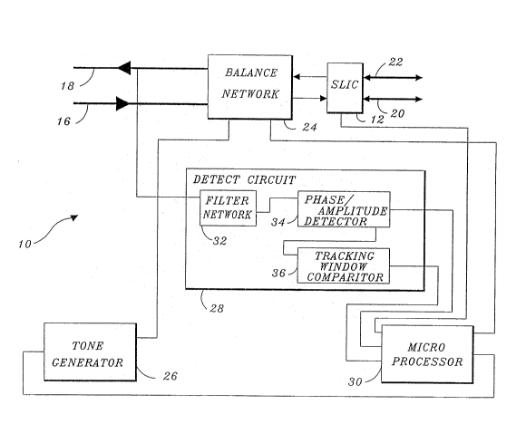
FIGURE 1 depicts in block diagram an autoequalizing hybrid 10 of this
invention including a subscriber loop interface circuit (SLIC) 12 for connecting a
15 four-wire communications path to a two-wire~communications path. The four-
wire communications path includes a two-wire communicatlons path 16 over which
slgnals are received by the~hybrid 10 and SLIC 12, and a two-wire communicationspath 18 over which signals are transmitted from the hybrid and the SLIC. The
SLIC 12 combines the signals from the two unidirectional paths 16 and 18 of the
20 four-wire path so that they can be transmitted and received over a bidirectional
two-wire path comprising a tip line 20 and a ring line 22 connected to the SLIC.The hybrid circuit 10 includes a~balance network 24 o~/er which a portion of
the receive path 16 signal is fed back to the transmit path 18~ to cancel any
sidetone signal that is re~lected by the SLlC 12 from th~. receive path 16. The
25 balance nètwork 24 h~s an adjustable impedance that is controlled by a
microprocessor 30. A tone generator 26 injects tones into the receive line 16 and
a detect circuit 28 that measures the reflected portions of the injected tones that
appear as sidetones on the transmit line 18. The microprocessor 30 monitors the
measurements made by the detect circuit 28 and in response, sets and resets the
30 impedance level of the balance letwork 24 to minimize the sidetone signal that is
emitted by the hybrid lO.
When the hybrid circuit 10 I first activated, the tone generator 26 injects a
set of equalization tones into rhe receive path 16. rhe microprocessor 30
monitors the measurements made by the detect circuit ~8 and, in response, sets,
35 or equalizes, the balance networK 24 feedback so as to minimize the level of the
returned signal. After equaliza-ion, the tone generator generates a supervisory
tone into the receive path 16. The detect circuit 28 and microprocessor 30
'. . . ~ '` "' ' '.,, `"',"' ~ " ' ' ' , ' '~ '
" ' .'. ~ '' "` '
:'',, ~ . ` , ~ ' ' '
" . , '
' ,' '~ " " :
`` 2 ~
--6--
monitor, or supervise, the performance of the balance network 24. When the
detect circuit 28 indicates an abrupt change in the level of the reflected
supervisory sidetone, the microprocessor 30 reequalizes the balance network 24.
The detect ~ircuit 28 includes a filter network 32 for extracting the
5 sidetones from the transmit path 18. The extracted sidetones are supplied to aphase/amplitude detector 34. During the equalization process, the
phase/amplitude detector 34 produces a balance signal that ind~cates when the
impedance for the equalization tones have been properly set. When the detect
circuit 28 is used to supervise the performance of the balance network 24, the
10 phase/amplitude detector 34 produces an amplitude signal indicative of the level
of the returned supervisory sidetone. The amplitude signal is supplied to a
tracking window comparator 36 that is sensitive to abrupt c~hanges in ~the
amplitude signal. Whenever an abrupt change in the amplitude signal is detected,the tracking window comparator~ 36 produces ~a recalibration signal. ~ The
15 microprocessor 30 responds to the recalibration signal by reequalizing the balance
network 24.
The schematic ~diagrams of ~ ~IGURES 2a ~ and` 2b~ illostrate the~ hybrld
circuit 10 of this ~ invention in detail. The balance network 24 includes a
processor-controlIed potentiometer 4b for controlling the level of the signals that
20 are received from ;the ~receive path l6. ~ The selectively attenuated receiye signals
are applied through a resistor 42 and through the inverting input~ of an amplifier 44
that functions as a feedback amplifier in~combination with resistor 46. The output
signals from the amplifier~44 are applied through a series-connècted capacitor 48
and a load resistor 50 to~a receive;input,~RxI, of the SLIC 12. A resistor 52 is tied
25 across the receive input and transmit output, TXo, of the SLIC 12 to provide a
termination impedance across the SLIC. Output signals from the SLIC 12 are
applied from the transmit output to a capacitor 54 and a resistor 56. Resistor 56
is connected ~ to the inverting input ~ of an ~ amplifier 58. Amplifier 58, in
combination with feedback resistor 60, provides the output signal that is emitted
30 over the transmit path 18.
The balance network 24 has three cancelation paths through which balancing
signals from the receive path 16 are applied~to the transmit path 18. A primary
path consists of resistor 66 and a processor controlled potentiometer 74. Resistor
- 66 is connected at one end to the wiper of potentiometer 74 and to the output of
35 amplifier 44 through series connected resistors 62 and 64. The other end of the
the primary cancelation path, the other end of resistor 66, is connected to the
inverting input of amplifier 58. A second cancelation path provides a balance
. ., . . : :. ,:,, .: ,.. - . - , . ; : . .
: . ~,- : .. ,: ., :,. : . . .: . , .
2 ~
-7 -
signal to compensate for excess high-frequency sidetone. The second, high-
frequency, cancelation path consists of a series-connected capacitor 68 and
resistor 70 that are selectively tied across resistor 66 by a processor-controlled
switch 72. The signals developed across primary and high frequency cancelation
5 paths are 180 out of phase with the sidetone signal. These signals are applied to
the inverting input of amplifier 58, the same input the transmit signal from theSLIC 12 is applied to, in order to cancel out the middle and high frequency
components (above approximately aoo Hz) of the sidetone signal.
The third cancelation path ls a low-frequency cancelation path comprised of
10 a conductor 78 selectively tied between the junction of resistors 62 and B4 and the
non-inverting input of amplifier 58. The low-frequency cancelation path further
includes a resistor 80 and a capacitor 82 both tied between conductor 78 and
ground. The low-frequency path is selectively tied between the junction of
resistors 62 and 64 by a processor-controlled switch 83. The signals developed
15 across the low-frequency cancelation path~ are applied to the non-inverting input
of amplifier 58 because they are in phase with the lo~-frequency components
(below approximately 200 Hz) of the reflected sidetone signals. When the low-
frequency cancelation path is enabled, amplifier 58 functions as a low-frequencydifferential amplifier that cancels out the low-frequency components of the
20 sidetone signal with in-phase low-frequency balanciDg signals. The level of the
cancelling signal which is applied through the balance network 24 is set by the
processor-controlled potentiometer 74 which which forms voltage dfvider that is
driven by the output signal of amplifier 44 and is tied to ground.
Tone generator 26 includes a processor-controlled square wave generator 79
25 capable of producing signals between~ I and 100 KHz. The output signals from the
square wave generator 79 are applied to a counter 84 that produces output signals
having a frequency of one-eighth the fnput signals. The output signals from the
counter 84 are applied to a processor-controlled level selector 85 that establishes
the voltage of the signals emitted by the tone generator 26. In the illustrated
30 embodiment of ~ the invention, the level selector 85 comprises a set of
resistors 86a, b, c, and d and a pair of NAND gates 87a and b connected to form a
processor-controlled step-level attenuator capable of emittfng an output signal at
three non-zero voltage levels. Two control signals are produced by the
- microprocessor 30 to control the output signal voltage level. In a preferred
35 embodiment of the invention, a level selector 85 need only to be capable of
emitting signals at two non-zero voltage levels.
-: `: . . - :: :
: ~ ~` ''. .: ,': ` '
":~ : :. , : ' ' ': ~: ` '
:~` 2~2~
--8--
A pull-up resistor 88 is connected between the signal generator level
selector 85 output and a positive voltage source--for example, a logic-level
source, VL. A pull-down resistor 89 is tied between the level selector 85 outputand ground. Resistors 88 and 89 establish a voltage divider to reduce the output5 amplitude from the level selector 85. The output signal from the level selector 85
is applied to DC blocking capacitor 90. Capaoitor 90 prevents DC voltages, whichcan be heard as a popping sound, from being applied to the balance network 24 and
the SLIC 12. The signal is then applied to the inverting input of amplifier 44
through a resistor 91.
A.s illustrated in FIGURI~ 2b, the detect circuit filter network 32 includes a
high-pass filter 94 connected to receive the output signal from the four-wire
transmit path 18. The high-pass filter 94 rejects low-frequency signals that result
from fluctuation in loop current. In a preferred embodiment of the ~invention, the
cutoff frequency for high-pass filter~94 is approximately 360 Hz. The output
15 signal from high-pass filter 94 is applied to both a low-pass~filter 96 and a band
pass filter 98. The low-pass filter attenuates ~high-frequency~ interference that
mày be present during the equalization ~process ~due to microphone background
noise, or voice signals that may ~be present durmg ~equalization.~ In a preferred
embodiment of the~invention, low-pass filter~96~ has a~ cutoff frequency of
20 approximately 3000 Mz.
Band pass filter 98 attenuates; signals, other than the réturned portion of the
superviso~ry signals, that may be present during~the~supervision process. The band
pass filter 98 primarily~ prevents voice; and/or~ data signals on the four-wire
transmit path 18 from~int~erfering~; with ~the moni~torlng of the supervisory signal.
25 The band pass filter 98 is centered on the supervisory signal frequency which is
above the normal range of signal a human can hear. In a preferred embodiment of
~ ~ the invention, the supervisory sidetone and band pass filter are centered on-~ ~ 18 KHz. Also, in a preferred embodiment of the invention, filters 94, 96 and 98
are ~ each active ~ filters formed from operationaI amplifiers and appropriately30 connected resistors and~capacitors (not iilustrated).
A processor-controlled switch 100 applies the output of either the low-pass
filter 96 or the band pass filter 98 to~ a commutative capacitor filter I02. Thecommutative capacitor filter 102 includes a resistor 104 and an amplifier 105
series-connected to switch 100. The resistor 104 is connected to the non-inverting
35 input of the amplifier 105. ~ resistor 106 provides a feedback loop between the
output of the amplifier 105 and the inverting input, and a resistor 108 is tied
between the inverting input and ground. Commutative capacitor filter 102 also
:
2 ~
g
includes a set OI eight identical capacitors 110a, b, c, . . . and h that are
selectively connected between the ampllfier 105 non-invertin~ input and ground.
An analog switch 112 ties each capacitor 110 a, b, c, . . . and h, one at a time,
between the amplifier 105 and ground. Switch 112 is controlled by the undivided
5 output signal from the square wave generator 79. The square wave generator 79
output signal causes the switch 112 to repetitively tie each capacitor 110a, b,
c, . .. h and ground during a specific moment during each cycle of the injected
signals. Consequently, the capacitors 110a, b, c, . . . and h integrate the current
flow through resistor 104 so that only the injected signals pass through the
10 commutative capacltor filter 102.
The phase/amplitude detector 34 includes an operational amplifier 116 that
produces signals representative of phase or amplitude of the reflected portion of
the injected signals. The signals from the filter network 32 are applied to the
non-inverting input of the operational amplifler 116 through series-connected
15 resistors 128 and 122. A capacitor 118 is connected to ground between
resistors 128 and 122. The signals from the filter network 32 are also applied to
the inverting input o~ amplifier 116 through series-connected resistors 124 and
126. A capacitor 120 is tied between resistors 124 and 126 and ground.
Resistors 128 and 124 have the same resistance. Capacitors~ 118 and 120 have
20 identical capacitance. A resistor 130 provides feedback between the output ofamplifier 116 and the inverting input. A resistor 132 is tied between the
amplifier 116 non-inverting inpu~ and ground. Resistors 122 and 132 have the
same resistance; resistors 126 and 130 also ~have the same resistance.
A processor-controlled actuated switch 134 toggles the application of the
25 filtered sidetone signals to the inputs of amplifier 116. The switch 134 is tied at
one end to output of the communicating capacitor filter 102 and at the other endto either resistor 128 or resistor 124. When the hybrid 10 is operated in the
equalization modeJ switch 134 is set by the divided clock signal Irom the
counter 84 so that it toggles in synchronization with the sidetone signal. When the
30 hybrid 10 is operated in the supervisory mode, switch 134 is set by a sidetone zero
crossing signal produced by a comparator 136. The inverting input of the
comparator 136 is connected to receive the sidetone signal from the commutative
capacltor filter 102, and a pull up resistor 138 is tied between the output of the
comparator 136 and the logic-level voltage source. A processor-controlled
35 switch 140 connects the blade control elements of switch 134 to either the output
of counter 84 or the output of the comparator 136.
: ~ ;, : . : -.
` ~2~
-10- ::
The output signal of amplifier 116 is applied to the non-inverting input on
comparator 142 to produce a signal indicative of hybrid balance. A pull-up
resistor 144 is tied between the output of comparator 142 and the logic level
voltage source. The comparator 142 and resistor 144 produce a balance signal
5 that is applied to the microprocessor 30. The balance signal is monitored by the
microprocessor 30 to determine the impedance setting of the balance network 24
during the equalization process.
The output signals from amplifier 116 are also applied to the tracking
window comparator 36. These signals represent the amplitude of the supervisory
lO signals that have been injected into the receive path 16 and been reflected out
through the transmit path 18. The tracking window comparator 36 includes an
amplifier 152 for producing a reference signal rèpresentative Oe the average
reflected supervisory signal level and an amplifier 1S4 for comparing the
instantaneous reflected sidetone signal level to the reference signal. Output
15 signals from amplifier 116~ are applied to the amplif~ier; 152 through a resistor 156
tied to the non-inverting input of the amplifier~ 152. Resistor 156 has a relatively
high resistanoe--for example, in ~ a preferred embodiment, approximately
lM ohms. ~ A capacitor~158 ;is tied between the non-inverting input of
; ~ ~ amplifier~ 154 and ground. A processor-controlled switch 160 is tied across
20 resistor 156 so that capacitor 158 can be charged to~an average reflected sidetone
signal level at the start of the supervision process. The output and inverting input
of amplifier 152 are tied together so~ that the amplifier functions as a unity gain
bufer amplifier that produces the reference sidètone amplitude signal.
Output signals from amplifier phase/amplitude~detector amplifier 116 are
25 also applied to the inverting input of amplifi~er 15~ through a resistor 162. The
reference signal Irom amplifier 152 is applied to the non-inverting input of the;~ ~ amplifier 154 through~a resistor 164i A feedback resistor 166 is tied between~ the
output of amplifier 154 and the inverting input. A resistor 168 is tied between the
non-inverting input of amplifier 154 and ground. Resistors 162 and 164 have the
30 same resistance as do resistors 166 and 168 so that amplifier 154 functions as a
differential amplifier that produces a~ supervisory sidetone tracking signal
representative o~ the difference between the instantaneous reflected sidetone
signals and the reference signal.
The supervisory sidetone tracking amplitude signal is applied to a pair o~
35 comparators 170 and 172 respectively that produce recalibration signals whenever
the supervisory tone tracking signal indicates there has been an abrupt change in
the level of the sidetone amplitude signal. The sidetone tracking signal is applied
2 ~ 2 ~
-11-
to the inverting input comparator 170 and the non-inverting input of
comparator 172. A pair of series-connected identical resistors 174 and 176 are
tied between the non-inverting input of comparator 170 and the in~erting input of
comparator 172. A resistor 178 is connected between the non-inverting input of
comparator 170 and a positive reference voltage, ~Vr. A resistor 180, identical to
resistor 178, tied between the inverting input of voltage ~Vr, is opposite
magnitude to the positive reference voltage. Resistors 174 and 178 and
resistors 176 and 180 form voltage dividers that respectively produce positive and
negative voltages that define the acceptable upper and lower limits for the
supervisory sidetone trackin~ signal. In a preferred embodiment of the invention,
resistors 174-180 are selected so that the voltage levels can be established by
using positive and negative logic level voltage sources as the reference voltagesources. A pull-up resistor 182 is tied betwsen the output of comparator 170 andthe logic level voltage source, and a pull-up resistor 184 is tied between the
output of comparator 172 ~nd the logic level voltage source. ~henever the
sidetone tracking signal exceeds the upper limit signal, the comparator 170
produces a recal high signal. Whenever the sidetone tracking signal falls below
the lower limit voltage, comparator 172 produces a recal low signal. The state of
the recal high and recal low signals are both monitored by the microprocessor 30.
Microprocessor 30 is a conventional 8-bit microprocessor. A suitable
microprocessor 30 is the 80C31 manufactured by Intel. In FIGURES 2a and 2b, the
signal input lines and the control output lines are shown as all being directly
connected to the microprocessor 30O In a preferred embodiment of the invention,
the microprocessor data signal input lines and control output lines are each
connected to latches that are selectively tied to a data bus connected to
input/output ports on the microprocessor 30. In one preferred embodiment of the
invention, a single latch is used to store the input data signals received by the
microprocessor 30; two latches are used to store the control si~nals produced by
the microprocessor.
Also shown in FIGURE 2a is a conductor 186 over which a hybrid enable
signal from the SLIC 12 to the microprocessor 30 travels. The hybrid enable
signal is the signal to the hybrid 10 that the circuit to which it is connected has
been activated and that it should start the first equalization process. In a
preferred embodiment of the invention, the enable signal is a hook status signal35 produced by the SLIC 12 and received by the microprocessor 30. The hook status
connector indicates the on/off hook status of the terminal device connected to the
SLIC 12. In other words, the hook status signal indicates whether or not the
: . ~, : , .
: , ,: ~ . : j
- ,:.. : . ~ ,:
`" 2~2~J~
-12-
terminal device has been actuated. Whenever the terminal device is off hook, or
actuated, the SLIC 12 produces an off hook signal. When the off hook signal is
initially produced, the microprocessor 30 directs the other components of the
hybrid 10 to perform the first equalization.
Hybrid equalization is performed by injecting equalization signals into the
four-wire receive path 16, determining the impedance needed to cancel the
reflected sidetone components of the in3ected signals and, based on the
impedances required for the individual signals, establishing ~inal Impedance forbalance network 24. In one preferred embodiment of the invention, three sidetone0 signals at 500 Hz, 1,000 Hz and 2,000 Hz are injected into the receive path 16 in
order to determine the appropriate balance network impedance level. The balance
network 24 impedance required to cancel each of the injected sidetone signals isdetermined by adjusting potentiometer 74 until the detect circuit 28 indicates
that the affeeted sidetone on the transmit path 18, instead of decreasing, starts to
15 increase. In other words, the detect circuit 28 produces the balance signal
whenever the sidetone level passes through a minimum, or null, level.
The balancing of an equalization signal starts with the microprocessor 30
directing the square wave generator 79 to produce the desired signal. The signalproduced by the square wave generator 79 is eight times the desired signal since20 this signal is subsequently divided by the counter 84 to produce the desired
signal. Microprocessor 30 sets switch 100 so that the output of the low pass
filter 96 is applied to the commutative capacitor filter 102 so that the reflected
equalization signal is extracted ~ from the transmit path 18 by the filter
network 32. The filtered ~ equalization signal is then applied to the
25 phase/amplitude detector 34.
The phase/amplitude detector 34 is operated as a phase detector to produce
a signal indicating when, as a result of sidetone passing through the null point, the
phase of the measured sidetone shifts. I~icroprocessor 30 sets switch 140 so that
ihe square wave produced by counter 84, which is at the equalization signal
30 frequeney, is used to toggle switch 134. Since switch 134 is toggled synchronously
with the equalization signal, opposite polarity charges accumulate on
capacitors 118 and 120. As balance network potentiometer 74 is cycled by the
microprocessor 30, the reflected equalization signal passes through the null point
and undergoes a phase reversal. The phase reversal causes capacitors 118 and 12035 to reverse charge and the signal produced by amplifier 116 to likewise changepolarity. Amplifier 142, which ~unctions as a comparator, in response to the
change in polarity of this output signal ~rom amplifier 116, produces the balance
.: . : ~ . :: -
-13-
signal to indicate that the impedance of the balance network 24 just crossed theimpedance level that minimized the level of the returned, unwanted sidetone.
The equalization of the balance network 24 by the sequential injection of
different equalization signals is explained in detail with reference to the flow5 chart of FIGURE 3. The equalization process starts with the microprocessor 30
setting potentiometer 40 so that the incoming signal received over the receive
path 16 is reduced by a factor of 16 as represented by step 200. The incoming
signals on the receive path are attenuated so that they do not distort the
equalization signals that are injected into the re~ceive path 16. ~fter the incoming
10 signal level has been attenuated, the 2~000 Hz sidetone is injected into a receive
path 16 as represented by step 202. At this s~age Oe the equalization process, the
signal generator level selector 85 is set so that the high voltage level sidetone is
injected into the receive path. This is done to rapidly saturate the elements
forming the balance network 24 so that the equalization process can occur in a
1j minimal amount of time. The microprocessor 30 then disables the low-frequencyand high-frequency compensating networks in a step 204 by opening switches 72
and 83.
After the high-voltage level sidetone signals have saturated the balance
network 24, the signaI generator level selector 85 is reset in a step 205 so that a
20 lower voltage level equalization signal is in~ected into the received path. The
lower level sidetone signal is used to establish the null during the equalization
process because it is less audible to the listener. Thus, prior to each balancing
step of the equalization processj the level selector ~5 is~first set to allow the
emission of a higher level voltage signal in order to saturate the balance
25 network 24- After saturation, the level selector 85 is reset so that the lessaudible lower level signal is emitted. ~or purposes of simplicity, the subsequent
resetting of the tone generator level selector 85 is neither described nor
illustrated.
After the equalization signal level is set, microprocessor 30 adjusts the
30 impedance of the balance network 24 to minimize the reflected equalization
signal as r~presented by balance step 206. The balance step 206 is performed by
the microprocessor 30 adjusting the balance network potentiometer 74 until the
phase/amplitude detector 34 produces the balancing signal which indicates that
the reflected equalization signal null point has been passed. During the last part
35 of the balancing step 206 and each subsequent balancing step, the
microprocessor 30 stores the wiper setting eor the balance network
potentiometer 74.
14 2 ~ &
:: ,
The microprocessor 30 then enables the high-frequency cancelation network
in a step 208 by closing the balance network switch 72. A balancing step 210 is
then performed wherein the microprocessor again adjusts potentiometer 74 to
reestablish the sidetone null point for the balance network 24.
Microprocessor 30 then diiects the tone generator 26 to produce the
1,000 Hz equalization signal as represented by step 212. The balance network
switch 72 is then opened to disable the high-frequency cancelation network in a
step 214. A balancing step 216 is then executed to reset the balance network 24
impedance. The high-frequency cancelation network is then reenabled in a
10 step 218 by the ¢losing of the balance network switch 72. A balancing step 220 is
then executed to reset the impedance of the balance network 24.
The microprocessor 30 then directs the tone generator 26 to produce a
500 Hz sidetone in a step 222. A balancing step 224 is then executed to reset the
impedance of the balance network 24. Note that when the 500 Hz signal is
15 produced, balance network switch 72 remains closed so that the high-frequencycancelation network remains enabled. The low-frequency composition network is
next enabled in a step 226 by the closing of the balance network switch 83. A
final balancing step 228 is then performed wherein the sidetone is adjusted withrespect to the 500 Hz sidetone signal and both the low-frequency and; high-
20 frequency cancelling networks enabled. ~
After the balancing steps have been executed, the potentiometer 74 wiper
settings are reviewed to control the enablement of the low-frequency and high-
frequency cancelling networks and thel setting of the balance network
potentiometer 74. Initially, a low-frequency cancelling network enablement
25 test 230 is executed to determine whether or not the Prequency cancelation
network should be enabled. This determination is made by comparing the
effectiveness of the balance network, as measured by the potentiometer 74
settingj in response to the application of different sidetones. The low-frequency
cancelation network is enabled if:
IE500 HF CANC E1,000 HF CA~CI >IE500 HF+LF CANC E1000 HF CANCI
where: E500 HF CANC is the balance network potentiometer 74 setting when the
500 Hz sidetone is injected into the receive path 16 and only the high-frequency35 cancelation network is enabled, E 500 HF+LF CANC jS the balance network
potentiometer 74 setting for the 500 Hz sidetone signal when both the high-
frequency and low-frequency cancelation networks are enabled, and E1 ooo HF
. , - , , . :
~ ` 2 ~
. .
- 1 S--
CANC is the balance network potentiometer 74 setting when ~ the 1,000 Hz
sidetone is injected and the high-frequency cancelation network is enabled. If the
low-frequency cancelation network is to be enabled, microprocessor 30 performs anetwork enablement step 232 wherein sWitch 83 is closed to enable the low-
5 frequency cancelation network.
Microprocessor 30 then determines whether or not the high-frequency
cancelation network should be enabled in a test 23~. A microprocessor 30
determines whether or not the high-erequency cancelation network should be
enabled by comparing the relative potentiometer 74 settings with and without the10 network enabled. The high frequency canoelation and network is enabled if:
~ ~ IE2000NOCANC-EI,OOONOCANCI~!E8000HFCANC-EIOOOHFCANCI
;- where E2000NO CANC 1s the potentiometer settlng when the~2000~Hz sidetone
15 signai is injected and the ~high-freguency cancelation network is disabled,
E10OONO CANC is the~balance~potentiometer setting when the ~1,000 ~Hz sidetone
is ~ ~ 1njected and t he ~ high-frequency cancelation ~ network is disabled, ~ and
E20ooHF CANC is the balanoe potentiom~eter setting when the 2000 Hz sidetone is
injected and the high-frequency cancelation network is enabled. lf the high-
frequency cancelation network is to be enabled, microprocessor ~30 closes the
balanoe network switch 72 in a ~step 236~ so as to enable the high-frequency~
cancelation network.
The setting ~of the balance~ network ~24 ~impedance concludes with the
resetting of the ~ balance ~ network potentiometer 74. The~ final setting of
25 ~ potentiometer 74 is dependent on whether or not the high-frequency cancelation
network is enabled as determined by test 234. ~1f the high-frequency cancelationnetwork is enabled, the microprocessor 30 sets the balance network
~; potentiometer 74~to the~ 1000 Hz high-frequency cancelation network enabled
~ ~ balance~setting adjusted for an overshoot factor asirepresented by step 238. If the
30 high-frequency cancelation network ~ is not enabled, the balance network
potentiometer 74 is reset to the lO00 Hz cancelation network disabled balanced
potentiometer setting adjusted Eor the overshoot eactor as represented by
step 240. The overshoot eactor compensates for the time lag between when the
equalization sidetone passes through the null signal level until the time that the
35 phase/amplitude detector 34 asserts a balance signal and the microprocessor 30
reads the balance network potentiometer 74 wiper setting.
' : : !
-` 2 ~ 2 ~
-16-
The last step in the equalization process is the restoration of the incoming
signal over the four-wire receive path 16 as represented by step 242. In the
restoration step 242, the microprocessor 30 resets potentiometer 40 so the full-strength signal is applied to receive sidetone components of the balance
5 network 24.
After the hybrld 10 is equalized, the mlcroprocessor 30 supervlses the
performance of the balance network 24. The microprocessor 30 directs the tone
generator 26 to produce a high-frequency, inaudible supervisory signal that is
injected into the receive path 16. The tone generator level selector 85 is set so
10 that the supervisory signal is produced at the second, or low level, signal
strength. Microprocessor 30 sets switch 100 so that the output of band
pass filter 98 is applied to the commutative capacitor filter 102. The filter
network 32 thus extracts the refiected supervisory tone component from the four-wire transmit path I8. During the~ supervision process, switch 140 ties the output
15 of comparator 136 to switch 134 so that the comparator toggles the switch 134.
The signal produced by comparator 136 toggles the switch 134 in synchronization
with the zero crossing of the sidetone signal. Opposite polarity voltages build up
in proportion to the amplitude of the tone on phase/amplitude detector
capacitors 118 and 120. Amplifier 116 consequently produces an output signal
20 proportional to the amplitude of the reflected supervisory signal.
The supervisory signal amplitude signal produced by the phase/amplitude
detector 34 is applied to the tracking window comparator 36. At the start of thesupervision process, microprocessor 30 momentarily closes switch 160 across
resistor 156 to allow capacitor i58 to charge to the full level of the supervisory
25 amplitude signal. Once switch 160 is open, amplifier 15~ functions as a buffer
amplifier that produces the reference sidetone amplitude signal.
The sidetone amplitude signal from the phase/amplitude detector 34 is also
applied to amplifier 154 that functions as a differential amplifier. As long as the
instantaneous sidetone amplitude signal approximates the reference sidetone
30 amplitude signal, amplifier 154 will produce a supervisory sidetone tracking signal
having a relatively low absolute voltage level. If changes in line impedance cause
a substantial increase in the level of the reflected signal, the level of the
supervisory sidetone tracking signal will similarly change. Any abrupt changes in
the supervisory sidetone will cause an abrupt change in the instantaneous sidetone
35 amplitude signal. Amplifier 154 will, in turn, produce a supervisory sidetonetracking signal having a relatively high absolute voltage level. When the
magnitude of the supervisory sidetone tracking signal passes the established upper
.: . . . .: . , .
..... ..
~: 2 ~
-17-
or lower limits, comparator 170 or 172 will produce an appropriate recal signal. In
response to the receipt of a recal signal, microprocessor 30 will then reequalize
the balance network 24 so as to minimi~e the level of signal that is reflected from
the four-wire receive path 16 to the transmit path 18.
The autoequalizing hybrid 10 of this invention initially adjusts the impedance
of the balance network 24 and monitors the performance o~ the network and, if
necessary, readjusts the balance network impedance to ensure the reflected
receive signal component of the four-wire transmit signal is as small as possible.
The hybrid 10 initially equalizes the balance network 24 when the terminal device
10 to which the hybrid is connected is first activated. The hybrid 10 then continues
to monitor, or supervise, the performance of the balance network 2~ to determinewhether or not the network continues to provide a cancelling signal that is
sufficient to minimize the reflected isidetone. Should line impedances or other
factors cause an increase in the reflected receive signal, as measured by a change
15 in the reflected supervisory signal, the balance network 24 of the hybrid 10 is
reegualized to minimize the reflected signal. For example, should line impedancechange because one terminal device is deactivated in favor of another device, ashappens when different telephones are placed on and off hook, the hybrid will
reequalize the balance network to compensate for the change. In other words,
20 the hybrid lO will prevent a sidetone singing signal from developing whenever one
telephone extension is deactivated in favor of another extension.
Moreover, just as this hybrid 10 can adjust for telephone extensions being
placed on and off hook, it can adjust for the connection and disconnection of
different terminal devices to the associated four-wire transmission equipment.
25 The hybrid 10 will automatically adjust the balance network to compensate for a
change in impedance whenever one terminal device, for example a facsimile
machine, is substituted for another terminal device, for example a computer
modem. The hybrid 10 will also adjust the balance network to compensate for
changes in incoming signal strength that may occur occur as consequence of
30 changes in the signal being emitted by the radiotelephone base station linked to
the remote terminal. The autoequalizing hybrid 10 of this invention is thus well-
suited to serve as an interface between standard two-wire telecommunications
terminal equipment and a radio that links the terminal equipment to a
conventional telecommunications network.
Another advantage of the hybrid 10 of this invention is that during the
equalization process the high-frequency equalization signal is the first signal
injected into the receive path 16. This signal serves as an indication to persons
, . , - , ~ - ~ .
2~2~
-18-
communicating over the hybrid 10 that the balance network 24 is reequalizing.
Upon hearing the signal, the persons will momentarily stop speaking so that low-frequency components of their speech do not distort the low-frequency
equalization signals injected into the receive path 16 as part of the equalization
5 process.
Moreover, the audio hybrid 10 of this invention determines the sidetone
signal null level impedance for a particular equalization tone based on the phase
reversal of the sidetone. Since the phase reversal occurs at the exact point thesidetone reaches the null level, this detection system offers an precise Indication
10 of when the null level is reached.
The foregoing description has been limited to a specific embodiment of this
invention. It will be apparent, however, from the description of the invention,
that it can be practiced using alternative components other than what have been
specifically described. For example, the disclosed components forming the
15 balance network 24, the tone generator 26, and the detect circuit 28 are readily
understood to be exemplary and not Iimiting. Moreover, it is further understood
that the disclosed process by which the microprocessor 30 establishes the balance
network 24 impedance similarly are illustrative and not limiting. For example, in
the disclosed embodiment of the~ invention, when either the recal high or recal low
20 supervisory signal is produced the same reequalization process is performed. In
other embodiments of the invention, different reequalization processes may be
executed depending upon whether it is the recal high or recal low signal that isreceived by the microprocessor 3û. Furthermore it is similarly understood that
the disclosed comparisons used to determine whether the high and low frequency
25 cancelation paths should be enable and the potentiometer 74 setting are similarly
only exemplary. In other embodiments of the invention, the potentiometer 74
settings, the equalization sidetone signal null level impedances, which form thecomponents of the comparison equations may differ greatly from what has been
disclosed.
Therefore, it is an object of the appended claims to cover all such
modifications and variations as come within the true spirit and scope of the
invention.