Note: Descriptions are shown in the official language in which they were submitted.
TRANSLATION OF PCT/JP90/00257
SPECIFICATION 2 ~ 2~ 1 2 5
INK JET HEAD HAVING HEAT GENERATING RESISTOR MADE OF NON-
SINGLE CRYSTALLINE SUBSTANCE CONTAINING Ir AND Ta AND INK
JET APPARATUS HAVING SUCH INK JET HEAD
FIELD OF THE INVENTION
This invention relates to an ink jet head and an ink
jet apparatus which include an electrothermal converting
body which is superior in resisting property to a shock of
a cavitation (hereinafter referred to as "cavitation
resisting property"), resisting property to erosion by a
cavitation (hereinafter referred to as "cavitation resist-
ing property"), chemical stability, electrochemical
stability, oxidation resisting property, dissolution
resisting property, heat resisting property, thermal shock
resisting property, mechanical durability and so forth. A
representative one of such ink jet heads and ink jet
apparatus includes an electrothermal converting body having
a heat generating resistor which generates, when energized,
heat energy which is to be directly applied to ink on a
heat acting face to cause the ink to be discharged. Then,
such electrothermal converting body is low in power
-- 1 --
2028 i 25
consumption and superior in responsibility to an input
signal.
BACKGROUND OF THE INVENTION
An ink jet system (in particular, a bubble jet system)
disclosed in U.S. Patent No. 4,723,129, U.S. Patent No.
4,740,796 and so forth can provide high speed, high density
and high definition recording of a high quality and is
suitable for color recording and also for compact design-
ing. Accordingly, progressively increasing attention has
been paid to such ink jet system in recent years. In a
representative one of apparatus which employ such system,
ink (recording liquid or the like) is discharged making use
of heat energy, and accordingly, it has a heat acting
portion which causes heat to act upon the ink. In parti-
cular, a heat generating resistor having a heat acting
portion is provided for an ink pathway, and making use of
heat energy generated from the heat generating resistor,
ink is heated suddenly to produce an air bubble by which
the ink is discharged.
The heat acting portion has, from a point of view of
causing heat to act upon an object, a portion apparently
similar in construction to a conventional so-called thermal
head. However, the heat acting portion is quite different
-
2028 1 2~
in fundamental technology from a thermal head in such
points that it contacts directly with ink, that it is
subjected to a mechanical shock which is caused by cavita-
tions produced by repetitions of production and extinction
of bubbles of ink, or in some cases, further to erosion,
that it is subjected to a rise and a drop of temperature
over almost 1,000 C for a very short period of time of the
order of 10 1 to 10 microseconds, and so forth. According-
ly, the thermal head technology cannot naturally be applied
to the bubble jet technology as it is. In other words, the
thermal head technology and ink jet technology cannot be
argued on the same level.
By the way, as for a heat acting portion of an ink jet
head, since it is subjected to such severe environment as
described above, it is a common practice to employ such a
structure that an electric insulating layer made of, for
example, SiO2, SiC, Si3N4 or the like is provided as a
protective film on a heat generating resistor and a cavita-
tion resisting layer made of Ta or the like is provided
further on the electric insulating layer in order to
protect the heat acting portion from environment in which
it is used. As composing materials of such protective
layer for use with an ink jet head, such materials which
are tough against a shock and erosion by a cavitation as
are described, for example, in U.S. Patent No. 4,335,389
2028 ~ 25
can be cited. It is to be noted that an abrasion resisting
layer made of Ta2O5 or the like popularly used for a
thermal head is not always superior in cavitation resisting
property.
Apart from this, it is desired for a heat acting por-
tion of an ink jet head to be constituted such that heat
generated from a heat generating resistor acts upon ink as
efficiently and quickly as possible in order to save power
consumption and improve the responsibility to an input
signal. To this end, apart from the aforementioned form in
which a protective layer is provided, also a form in which
a heat generating resistor contacts directly with ink is
proposed in Japanese Patent Laid-Open No. 126462/1980.
A head of the form is superior with regard to thermal
efficiency to the form in which a protective layer is
provided. However, not only a heat generating resistor is
sujected to a shock or erosion by a cavitation and further
to a rise and a drop of temperature, but also it is
subjected to an electrochemical reaction which is caused by
electric current which flows through recording liquid
because the recording liquid which contacts with the heat
generating resistor has an electric conductivity.
Consequently, various metals, alloys, metallic compounds or
cermets beginning with Ta2N and RuO2 which are conven-
tionally known as materials of heat generating resistors
2028 1 25
are not always satisfactory in durability or stability for
an application to a heat generating resistor of a head of
the form.
While some of ink jet heads of the form wherein a
protective layer is provided as described above which have
been proposed so far can be adopted in practical use as
regards durability and resistance variation, it is very
difficult, in any case, to perfectly prevent occurrence of
defects which may take place upon formation of a protective
layer, which is a serious factor of deteriorating the yield
in mass production. Then, further improvement in speed and
density in recording is demanded, and since there is a
tendency that the number of discharging outlets of a head
is increased corresponding to such demand, this is a
serious problem.
Further, while a protective layer described above
decreases the efficiency in transfer of heat from a heat
generating resistor to recording liquid, if the heat
transfer efficiency is low, then the entire power consump-
tion required increases and the temperature variation of
the head upon driving increases. Such temperature
variation results in volume variation of a droplet dis-
cn L~ ~ES
A charged from a discharging outlet, which ~ ]~o~ ~ c~o of a
variation in density of an image. Meanwhile, if the number
of discharging operations per unit time is increased in
2~2~ ~ 25
order to cope with an increase in recording speed, the
power consumption by the head is increased accordingly and
the temperature variation is increased. Such temperature
variation will bring about a corresponding density varia-
tion of an image obtained. Also when an increase in number
of discharging outlets which involves an increase in
density of electrothermal converting bodies, the power
consumption by the head increases, and a temperature varia-
tion by such increase in power consumption will likewise
cause an image obtained to have a density variation cor-
responding to such temperature variation. Such problem
that an image obtained has a density variation is contrary
to a demand for a high quality of a recorded image and is
required to be solved as early as possible.
In order to solve such problem, provision is desired
earnestly of an ink jet head wherein a heat generating
resistor contacts directly with ink and the heat efficiency
is high.
However, since a heat generating resistor of an ink
jet head of the conventional form wherein ink contacts
directly with the heat generating resistor is subjected not
only to a shock or erosion by a cavitation and further to a
rise and a drop of temperature but also to an electrochemi-
cal reaction as described hereinabove, conventional
materials for a heat generating resistor such as Ta2N, Ru02
2028 1 25
or HfB2 have a problem in durability in that the heat
generating resistor may be mechanically destroyed, or
corroded or dissolved.
The materials which are disclosed as tough against a
shock or erosion by a cavitation in U.S. Patent No.
4,335,389 and so forth do not exhibit their effects if they
are not used for such a protective layer (cavitation
resisting layer) as described hereinabove. However, if any
of the materials is employed for a heat generating resistor
which contacts directly with ink, then it is sometimes
dissolved or corroded by an electrochemical reaction, and
consequently, it may not assure a sufficient durability.
Further, the stability of discharging is inevitable
for recording of a high definition and a high quality, and
to this end, it is necessary that the resistance variation
of a heat generating resistor be low, and for practical
use, preferably it is lower than 5~. Ta or a Ta-Al alloy
mentioned in Japanese Patent Laid-Open No. 96971/1984 is
comparatively superior, where it is employed for a heat
generating resistor of an ink jet heat which contacts
directly with ink, in durability, that is, in cavitation
resisting property in that the resistor is not broken.
However, with regard to a resistor variation during a
repetition of production of bubbles, Ta or a Ta-Al alloy is
not satisfactory in that the resistor variation is not very
2028 1 25
small. Further, Ta or a Ta-Al alloy does not have a very
high ratio M between an applied pulse voltage (Vbreak) at
which the resistor is broken and a bubble producing
threshold voltage (Vth) and is not very high in heat
resisting property, and consequently, they have a problem
that the life of the resistor is deteriorated significantly
by a small increase of a driving voltage (VOp). In
particular, Ta or a Ta-Al alloy is not always sufficiently
high in resisting property to an electrochemical reaction,
and consequently, where it is employed as a material for a
heat generating resistor for an ink jet head which contacts
directly with ink, if production of bubbles is repeated by
a large number of application pulses, then the electric
resistance of the heat generating resistor is varied to a
great extent. Thus, there is a problem that also the
condition of production of bubbles is varied by such varia-
tion of the electric resistance of the heat generating
resistor. Further, there is another problem that, since
the heat resisting property is not very high, a small
variation of VOp sometimes has a significant influence on
the life of the resistor.
In this manner, even if a heat generating resistor
which contacts with recording liquid (that is, ink) is
formed from any of the conventionally known materials, an
ink jet head or an ink jet apparatus cannot be obtained
2028 1 25
readily which can satisfy all of a cavitation resisting
property, erosion resisting property, mechanical durabi-
~ 6~C~
lity, eh~ic~l stability, electrochemical stability,
resistance stability, heat resisting property, oxidation
resisting property, dissolution resisting property and
thermal shock resisting property.
Particularly, an ink jet head or an ink jet apparatus
cannot be obtained readily which has a structure wherein a
heat generating resistor is provided for direct contact
with ink and is high in heat transfer efficiency, superior
in signal responsibility and sufficiently high in
durability and discharging stability.
SUMMARY O F THE I NVENT I ON
It is a principal object of the present invention to
provide an improved ink jet head which solves the above
described problems of a conventional ink jet head of the
form wherein ink contacts directly with a heat generating
resistor as well as an ink jet apparatus having such
improved ink jet head.
It is another object of the present invention to
provide an improved ink jet head which is superior in
cavitation resisting property, erosion resisting property,
mechanical durability, chemical stability, electrochemical
-
2028 1 25
stability, resistance stability, heat resisting property,
oxidation resisting property, dissolution resisting pro-
perty and thermal shock resisting property and has a high
thermal conductivity.
It is a further object of the present invention to
provide an improved ink jet head which has a structure
wherein a heat generating resistor contacts directly with
recording liquid (that is, ink) and in which, even after
repetitive use for a long period of time, heat energy is
transmitted always stably in a high efficiency to the
recording liquid rapidly in response to a signal on demand
to effect discharging of the ink to produce an excellent
recorded image.
It is a still further object of the present invention
to provide an improved ink jet head which has a structure
wherein a heat generating resistor contacts directly with
recording liquid and in which the power consumption by the
heat generating resistor is restricted low to minimize the
temperature variation of the head and, even after repeti-
tive use for a long period of time, discharging of ink is
effected always stably to obtain an image which is free
from a variation in density caused by a temperature
variation of the head.
It is a yet further object of the present invention to
provide an ink jet apparatus which includes such an
-- 10 --
2028 1 25
improved ink jet head as described above.
BRIEF DESCRIPTION OF THE DRAWINGS
Fig. l(a) is a schematic front elevational view of
essential part of an example of an ink jet head of the
present invention as viewed from a discharging outlet
side.
Fig. l(b) is a schematic sectional view taken along
alternate long and short dash line X-Y of Fig. l(a).
Fig. l(c) is a schematic plan view of a base member
for an ink jet head at a stage at which a layer of a heat
generating resistor and electrodes are provided, and
Fig. l(d) is a schematic plan view of the base
member for an ink jet head at another stage at which a
protective layer 6 is provided on those layers.
Fig. 2 is a schematic sectional view showing another
example of a base member for use with an ink jet head
according to the present invention.
Figs. 3(a) and 3(b) are a schematic top plan view
and a sectional view, respectively, individually showing
other examples of an ink jet head according to the
present invention.
Fig. 4 is a schematic sectional view showing an
example of a high frequency sputtering apparatus which is
used to produce a film of a heat generating resistor or
the like according to the present invention; and
Fig. 5 is an appearance perspective view showing an
example of an ink jet apparatus according to the present
invention.
11
' ~3
2028 1 2~
- DESCRIPTION OF THE INVENTION
The inventors have determined, after an extensive
investigation of possible solutions to the above
described problems of a conventional ink jet head, of the
type wherein ink contacts directly a heat generating
resistor and with a view to achieving the objects
described above, that an ink jet head which attains the
objects can be obtained if the heat generating resistor
of the ink jet head is made of a non-single crystalline
material which consists essentially of iridium (Ir) and
tantalum (Ta) in a specific range of proportions, and the
present invention depends upon this observation.
The non-single crystalline material is an amorphous
material, a polycrystalline material or a material
consisting of an amorphous material and a polycrystalline
material in a mixed state, which contains two elements of
iridium (Ir) and tantalum (Ta) in the proportions of 35
to 77 atom percent and 23 to 65 atom percent,
respectively (these materials will be hereinafter
referred to as "non-single crystalline Ir-Ta substance"
or "Ir-Ta" alloy).
The inventors selected iridium (Ir) from a point of
view of a substance which is high in heat resisting
property and oxidation resisting property and is
chemically stable and selected tantalum (Ta) from a point
of view of a substance which has a mechanical strength
and provides
llA
2028 1 25
oxides which are high in dissolution resisting property to
a solvent, and then produced a plurality of non-single
crystalline substance samples containing the two elements
at predetermined composition rates by sputtering.
The individual samples were produced by forming a film
on a single crystalline Si substrate or a Si single
crystalline substrate with a thermally oxidized SiO2 film
of 2.5 um thick formed on a surface thereof using a sput-
tering apparatus (commodity name: sputtering apparatus CFS-
8EP, manufactured by Kabushiki Kaisha Tokuda Seisakusho)
shown in FIG. 4. Referring to FIG. 4, reference numeral
201 denotes a film forming chamber. Reference numeral 202
denotes a substrate holder disposed in the film forming
chamber 201 for holding a substrate 203 thereon. The
substrate holder 202 has a heater (not shown) built therein
for heating the substrate 203. The substrate holder 202 is
supported for upward and downward movement and also for
rotation by means of a rotary shaft 217 extending from a
drive motor (not shown) installed outside the system. A
target holder 205 for holding thereon a target for the
formation of a film is provided at a position in the film
forming chamber 201 opposing to the substrate 203.
Reference numeral 206 denotes a Ta target formed from a Ta
plate placed on a surface of the target holder 205 and
having a purity of higher than 99.9 weight percent.
- 12 -
-
2028 1 25
Reference numeral 207 denotes an Ir target formed from an
Ir sheet placed on the Ta target and having a purity of
higher than 99.9 weight percent. A plurality of such Ir
targets`each having a predetermined area are disposed in a
predetermined spaced relationship on a surface of the Ta
A\ ~ target 206 as denoted by 207 and ~ in FIG. 4. The areas
and positions of the individual Ir targets 207 and 208 are
determined in accordance with calibration curves produced
in accordance with a result of ascertainment which has been
made in advance of how a film which contains desired Ir and
Ta at a predetermined composition rate can be obtained from
a relationship of a ratio of areas of the two targets.
Reference numeral 218 denotes a protective wall for
covering over side faces of the Ta target and Ir targets so
that they may not be sputtered by plasma from the side
faces thereof. Reference numeral 204 denotes a shutter
plate provided for horizontal movement such that it cuts
off the space between the substrate 203 and the targets at
a position above the target holder 205. The shutter plate
204 is used in the following manner. In particular, before
starting of film formation, the shutter plate 204 is moved
to a position above the target holder 205 on which the Ta
target and Ir targets are carried, and then inert gas such
as argon (Ar) gas is introduced into the inside of the film
forming chamber 201 by way of a gas supply pipe 212. Then,
20~8 1 25
an RF power is applied from an RF power source 215 to
convert the gas into plasma so that the Ta target and Ir
targets are sputtered by the plasma thus produced to remove
impurities from surfaces of the individual targets. After
then, the shutter plate 204 is moved to another position
(not shown) at which it does not interfere with film
formation.
The RF power source 215 is electrically connected to a
surrounding wall of the film forming chamber 201 by way of
a conductor 216, and it is electrically connected also to
the target holder 205 by way of another conductor 217.
Reference numeral 214 denotes a matching box.
A mechanism (not shown) for internally circulating
cooling water so that the Ta target and Ir targets may be
maintained at a predetermined temperature during film
formation is provided on the target holder 205. An exhaust
pipe 210 for exhausting air from within the film forming
chamber is provided for the film forming chamber 201, and
the exhaust pipe is communicated with a vacuum pump (not
shown) by way of an exhaust valve 211. Reference numeral
202 denotes a gas supply pipe for introducing sputtering
gas such as argon gas (Ar gas) or helium gas (He gas) into
the film forming chamber 201. Reference numeral 213
denotes a flow rate adjusting valve for sputtering gas
provided for the gas supply pipe. Reference numeral 209
-
2028 1 25
denotes an insulating porcelain-clad interposed between the
target holder 205 and a bottom wall of the film forming
chamber 201 for electrically isolating the target holder
205 from the film forming chamber 201. Reference numeral
219 denotes a vacuum gage provided for the film forming
chamber 201. An internal pressure of the film forming
chamber 201 is detected automatically by the vacuum gage.
While the apparatus shown in FIG. 4 is of the form
wherein only one target holder is provided as described
above, a plurality of target holders may otherwise be
provided. In this instance, the target holders are
arranged in an equally spaced relationship on concentric
circles at locations opposing to the substrate 203 in the
film forming chamber 201. Then, individually independent
RF power sources are electrically connected to the
individual target holders by way of individual matching
boxes. In the case of the arrangement described above,
since two kinds of targets, that is, an Ir target and a Ta
target, are used, the two target holders are disposed in
the film forming chamber 201 as described above, and the
targets are individually placed on the respective target
holders. In this instance, since predetermined RF powers
can be applied to the individual targets independently of
each other, the composition rate of the film forming
elements for the film formation can be varied to form a
2028 ~ 25
film wherein one or both of the elements of Ir and Ta are
varied in the film thicknesswise direction.
Production of the individual samples using the
apparatus shown in FIG. 4 was performed in the following
film forming conditions except that, each time a sample was
to be produced, placement of the Ir targets 207 and 208 on
the surface of the Ta target 206 was performed with
reference to calibration curves prepared in advance for a
non-single crystalline substance (film) having a predeter-
mined composition rate of Ir and Ta to be obtained.
Substrates placed on the substrate holder 202:
Si single crystalline substrate of a 4 inch 0 size
(manufactured by Wacker) (one piece) and Si single
crystalline substrate of a 4 inch 0 size having a
SiO2 film of 2.5 um thick formed thereon (manu-
factured by Wacker)(three pieces)
Substrate set temperature : 50C
Base pressure : 2.6 x 10 Pa or less
High frequency (RF) power : 1,000 W
Sputtering gas and gas pressure: argon gas, 0.4 Pa
Film forming time : l2 minutes
An electron probe microanalysis was performed to
effect a component analysis of some of those of the samples
obtained in such a manner as described above which were
produced each by forming a film on a substrate with a SiO2
- 16 -
20~8 1 2~
film using EPM-810 manufactured by Kabushiki Kaisha Shimazu
Seisakusho, and then those samples which were produced each
by forming a film on a Si single crystalline substrate were
observed for crystalline structure by means of an X-ray
diffraction meter (commodity name: MXP3) manufactured by
Mac Science. Subsequently, using some of those of the
remaining samples which were produced each by forming a
film on a substrate with a SiO2 film, a so-called pond test
was conducted for observing a resisting property to an
electrochemical reaction and a resisting property to a
mechanical shock, and further, using the remaining ones of
the samples which were produced each by forming a film on a
substrates with a SiO2 film, a step stress test (SST) was
conducted for observing a heat resistor property and a
shock resisting property in the air. The pond test men-
tioned above was conducted by a similar technique as in a
"bubble resisting test in low conductivity ink" which will
be hereinafter described except that, as liquid for the
immersion, liquid was used consisting of sodium acetate
dissolved by 0.15 weight percent in solution consisting of
70 weight parts of water and 30 weight parts of diethylene
glycol. The SST mentioned above was conducted by a
technique similar to that of a "step stress test" which
will be hereinafter described. The following results were
obtained by a synthetic examination of results of the pond
2028 1 25
obtained by a synthetic examination of results of the pond
test and results of the SST. In particular, it became
clear with most preferable samples that each of them
consists for the most part of a polycrystalline substance
and also contains a substance consisting of a polycrystal-
line substance and an amorphous substance in a mixed
condition and also an amorphous substance. Subsequently,
when a composition rate of Ir and Ta was investigated with
samples within a preferable range, it was found out that
they include 35 to 77 atom percent of Ir and 23 to 65 atom
percent of Ta. Similarly, as regards samples within a more
preferable range, it was found out that they include 42 to
77 atom percent of Ir and 23 to 58 atom percent of Ta.
Further, as regards the samples within the most preferable
range, it was found out that they include 42 to 77 atom
percent of Ir and 23 to 40 atom percent of Ta.
From the results described above, the inventors
ascertained that a non-single crystalline Ir-Ta substance
containing Ir and Ta as essential components at the
respective composition rates given below is suitable for
use for a heat generating resistor of an ink jet head:
35 atom ~ _ Ir _ 77 atom %, and
23 atom ~ < Ta < 65 atom ~.
Further, the inventors made heat generating resistors
using such non-single crystalline Ir-Ta substances and
- 18 -
clear. 20~8 1 25
In particular, where any of the non-single crystalline
Ir-Ta substances is employed, an ink jet head having a heat
generating resistor can be obtained which is superior not
only in cavitation resisting property and erosion resisting
property but also in electrochemical and chemical stability
and heat resisting property. Particularly, an ink jet head
can be obtained of the construction wherein a heat generat-
ing portion of a heat generating resistor contacts directly
with ink in an ink pathway. In a head of the construction,
since heat energy produced from the heat generating section
of the heat generating resistor can act directly upon the
ink, the heat transfer efficiency to the ink is high.
Therefore, the power consumption by the heat generating
resistor can be restricted low, and the rise of temperature
of the head (temperature variation of the head) can be
reduced significantly. Consequently, occurrence of a
density variation in an image by a temperature variation of
the head can be eliminated. Besides, a further high
responsibility to a discharging signal applied to the heat
generating resistor can be obtained.
Further, with a heat generating resistor according to
the present invention, a desired specific resistance can be
obtained with a high controllability such that a dispersion
in resistance in a single head can be reduced very small.
- 19 -
-
2028 1 25
Accordingly, an ink jet head can be obtained which can
effect significantly stabilized discharging of ink compar-
ing with a prior art arrangement and is superior also in
durability.
An ink jet head having such superior characteristics
as described above is very suitable to achieve high speed
recording of a high image quality involved in increase of
discharging,outlets.
DETAILED DESCRIPTION OF PREFERRED FORMS
Accordingly, one form of the present invention
provides an ink jet head which includes an electrothermal
3~o~
converting body having a heat generating rogictnr which
-generates, upon energization, heat energy to be directly
applied to ink on a heat acting face to discharge the ink,
characterized in that the heat generating resistor is
formed from a non-single crystalline substance substan-
tially composed of Ir and Ta and containing such Ir and Ta
at the following respective composition rates:
35 atom percent _ Ir < 77 atom percent, and
23 atom percent < Ta < 65 atom percent.
Another aspect of the present invention provides an
ink jet head which includes an electrothermal converting
~65~
body having a heat generating ~^g;~tor which generates,
- 20 -
2028 1 25
upon energization, heat energy to be directly applied to
ink on a heat acting face to discharge the ink, charac-
terlzed in that the heat generating resistor is formed from
a non-single crystalline substance substantially composed
of Ir and Ta and containing such Ir and Ta at the following
respective composition rates:
42 atom percent _ Ir _ 77 atom percent, and
23 atom percent _ Ta _ 58 atom percent.
A further aspect of the present invention provides an
ink jet head which includes an electrothermal converting
p.,6S IS~
ody having a heat generating rogi~tc~ which generates,
upon energization, heat energy to be directly applied to
ink on a heat acting face to discharge the ink, charac-
terized in that the heat generating resistor is formed from
a non-single crystalline substance substantially composed
of Ir and Ta and containing such Ir and Ta at the following
respective composition rates:
60 atom percent _ Ir _ 77 atom percent, and
23 atom percent _ Ta < 40 atom percent.
In the present invention, while reasons why such
various remarkable effects as described hereinabove are
achieved where a heat generating resistor for an ink jet
head is formed from any of the specific non-single
crystalline Ir-Ta substances described above, it is
imagined that one of the reasons is that Ir which is
- 21 -
2028 1 25
superior in heat resisting property, oxidation resisting
property and chemical stability prevents a reaction; Ta
provides a mechanical strength and brings about a dis-
solution resisting property; and coexistence of the two
elements at the specific composition rates make the stress
optimum and increases the adhesion and toughness.
The inventors have confirmed by way of an experiment
that, where a heat generating resistor for an ink jet head
is formed using a non-single crystalline Ir-Ta substance
other than the specific non-single crystalline Ir-Ta
substances described above (that is, amorphous Ir-Ta alloy,
polycrystalline Ir-Ta alloy or mixture of the alloys), the
following problems are presented.
In particular, such heat generating resistor is not
optimum in cavitation resisting property, erosion resisting
property, electrochemical stability, chemical stability,
heat resisting property, adhesion, internal stress and so
forth, and where it is used as a heat generating resistor
for an ink jet head, particularly as a heat generating
resistor of the type wherein it directly contacts with ink,
sufficient durability is not obtained. For example, where
the amount of Ir is excessively great, exfoliation of a
film sometimes takes place, and on the contrary where the
amount of Ta is excessively great, the resistor variation
sometimes becomes great.
-
2028 1 25
In the present invention, since a heat generating
resistor is formed from one of the specific non-single
crystalline Ir-Ta substances described above, there is no
necessity of provision of a protective film, and an ink jet
head can be constructed to be of the type wherein a heat
generating portion of the heat generating resistor contacts
directly with ink in an ink pathway. Then, the ink jet
head according to the present invention is free from the
problems which can be seen with the conventionally proposed
ink jet heads which have a heat generating resistor which
contacts directly with ink, but has the following various
advantages which cannot be forecast from the prior art. In
particular, (i) it is superior in cavitation resisting
property, erosion resisting property, mechanical durabili-
ty, chemical stability, electrochemical stability,
resistance stability, heat resisting property, oxidation
resisting property, dissolution resisting property and
thermal shock resisting property and has a superior heat
conductivity; (ii) whatever type recording liquid (that is,
ink) is employed, the ink jet head transmits heat energy
efficiently to the recording liquid to effect discharging
of the ink to produce a superior record image in quick
response to an on demand signal always with stability even
after a repetitive use for a long period of time; and then,
(iii) the power consumption by the heat generating resistor
- 23 -
20281 25
is restricted low to minimize the temperature variation of
the head, and even after a repetitive use for a long period
of time, the ink jet head carries out discharging of ink
always with stability to produce an image which is free
from a density variation by a temperature variation of the
head.
In a preferred form of an ink jet head according to
the present invention, a heat generating resistor thereof
is formed from any of the specific polycrystalline Ir-Ta
substances described above and is constructed in a form
wherein a heat generating portion of the heat generating
resistor contacts directly with ink in an ink pathway. In
this instance, the condition stability and the resistance
stability are particularly prominent.
While the thickness of a layer of the heat generating
resistor in the present invention is determined suitably so
that suitable heat energy may be produced effectively,
preferably it is 300 A to 1 ~m, and more preferably, it is
O O
1,000 A to 5,000 A from the point of durability or
characteristics in production and so forth.
Further, in the present invention, while a heat
generating resistor formed from any of the specific non-
single crystalline Ir-Ta substances described above is
normally of the form of a single layer structure, it may
otherwise be of the form of a multi-layer structure in some
2028 1 25
cases. Further, with regard to a layer constituting a heat
generating resistor and made of any of the non-single
crystalline Ir-Ta substances, it is not always necessary
that the composition of the two elements composing the
substance, that is, Ir and Ta, be uniform over the entire
area of the layer. In particular, one or both of the two
elements may be distributed non-uniformly in the thickness-
wise direction of the layer so far as the composition rate
of the individual elements of Ir and Ta remains within any
of the specific ranges described hereinabove. For example,
where a heat generating resistor is of the form of a single
layer structure, the non-single crystalline Ir-Ta substance
which forms the layer may be formed such that one of the
components thereof is distributed at a comparatively high
rate in a region of the layer adjacent a base member for
the ink jet head.
On the other hand, a heat generating resistor is made
in a two layer structure wherein two layers of a non-single
crystalline Ir-Ta substance are layered and one of the two
layers which is positioned adjacent a base member for the
ink jet head is constituted such that one of the components
is distributed at a comparatively high rate in a region of
the layer adjacent the base member.
Further, while generally a surface or the inside of a
layer is sometimes oxidized upon touching with the
- 25 -
20~8 1 25
atmospheric air or in a procedure of production, the
effects of a material according to the present invention
are not deteriorated by such little oxidation of a surface
or the inside of the material. As such an impurity, at
least one element selected, for example, from, beginning
with O by oxidation described above, C, N, Si, B, Na, Cl
and Fe can be cited.
In addition, a heat generating resistor according to
the present invention can be formed, for example, by a DC
sputtering method wherein individual materials are piled up
simultaneously or alternately, an RF sputtering method, an
ion beam sputtering method, a vacuum deposition method, a
CVD method, or a film forming method wherein application
and baking of paste containing organic metal, or the like
are performed.
Subsequently, an ink jet head according to the present
invention which employs an alloy material having any of the
compositions described above as a heat generating resistor
and is superior in thermal efficiency, signal responsibili-
ty and so forth will be described with reference to the
drawings.
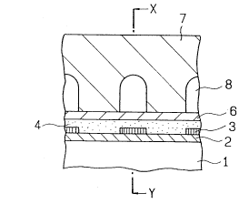
FIG. l(a) is a schematic front elevational view of a
principal portion of an example of an ink jet head of the
present invention as viewed from a discharging outlet side;
and FIG. l(b) is a schematic sectional view taken along
- 26 -
2028 1 25
alternate long and short dash line X-Y in FIG. l(a).
The ink jet head of the present example has a basic
construction wherein an electrothermal converting body
having a layer 3 for heat generating resistors having a
predetermined shape and electrodes 4 and 5 is formed on a
support body which includes a lower layer 2 provided on a
surface of a substrate 1, and a protective layer 6 for
covering at least the electrodes 4 and 5 of the electro-
thermal converting body is layered, and besides a grooved
plate 7 having recessed portions for providing liquid
pathways 11 communicating with discharging outlets 8 is
joined over the protective layer 6.
The electrothermal converting body of the present
example has the heat generating resistor 3, electrodes 4
and 5 connected to the heat generating resistor 3, and
protective layer 6 provided in accordance with the
necessity. Meanwhile, a base member for the ink jet head
has the support body having the substrate 1 and the lower
layer 2, the electrothermal converting body, and the
protective layer 6. In the case of the head of the present
example, a heat acting face 9 which transmits heat directly
to ink is substantially same as a face of a portion (heat
generating portion) of the heat generating resistor 3 which
is disposed between the electrodes 4 and 5 and contacts
with ink, and corresponds to a portion of the heat
-
2028 1 25
generating portion which is not covered with the protective
film 6.
The lower layer 2 is provided in accordance with the
necessity and has a function of adjusting the amount of
heat to escape to the substrate 1 side and transmitting
heat generated by the heat generating portion efficiently
to ink.
The electrodes 4 and 5 are electrodes for energizing
the layer 3 of the heat generating resistor to cause heat
to be generated from the heat generating portion, and in
the present example, the electrode 4 is a common electrode
to individual heat generating portions while the electrode
5 is a selecting electrode for individually energizing each
of the heat generating portions.
The protective layer 6 is provided in accordance with
the necessity for preventing the electrodes 4 and 5 from
contacting with and being chemically corroded by ink or
preventing the electrodes from being short-circuited by way
of ink.
It is to be noted that FIG. l(c) is a schematic plan
view of the base member for an ink jet heat at a stage
wherein the layer 3 and electrodes 4 and 5 of the heat
generating resistor are provided. Meanwhile, FIG. l(d) is
a schematic plan view of the base member for an ink jet at
another stage wherein the protective layer 6 is provided on
- 28 -
the layers of them. 2a28 1 25
In the present ink jet head, since an alloy material
of any of the compositions described above is employed for
the layer 3 of the heat generating resistor, while the ink
jet head has a construction wherein the ink and the heat
acting face 9 contact directly with each other, it has a
good durability. In this manner, where a construction is
employed wherein a heat generating portion of a heat
generating resistor serving as a heat energy source
contacts directly with ink, heat generated by the heat
generating portion can be transmitted directly to the ink,
and very efficient heat transmission can be achieved
comparing with an ink jet head of another construction
wherein heat is transmitted to ink by way of a protective
layer or the like.
As a result, the power consumption by the heat
generating resistor can be restricted low, and also the
degree in rise of temperature of the head can be reduced.
Further, the responsibility to an input signal (discharging
instruction signal) to the electrothermal converting body
is improved, and a bubble producing condition necessary for
discharging can be obtained stably.
Construction of an electrothermal converting body
having a heat generating resistor formed using an alloy
material according to the present invention is not limited
- 29 -
2028 1 25
to the example of FIG. 1 but may have various forms, for
example, such a construction as shown in FIG. 2.
The base member for an ink jet head having the
construction of FIG. 2 does not require provision of a
protective layer for an electrode because the electrodes 4
and 5 are covered with the layer 3 of the heat generating
resistor of the alloy material of any of the compositions
described hereinabove.
Further, also the construction of the discharging
outlet and liquid pathway of the ink jet head is not
limited to such construction as shown in FIGs. l(a) and
l(b) wherein the direction in which ink is supplied to the
heat acting face 9 and the direction in which ink is dis-
charged from the discharging outlet 8 making use of heat
energy generated from the heat generating portion are
substantially the same, but may be of another construction
wherein the directions are different from each other. For
example, it is possible to employ such a construction as
shown in FIGs. 3(a) and 3(b) wherein the two directions
make a substantially right angle, or the like. Reference
numeral 10 in FIG. 3 denotes a plate (discharging outlet
plate) of a suitable thickness in which discharging outlets
are provided, and reference numeral 12 denotes a support
wall member for supporting the discharging outlet plate
thereon.
- 30 -
2028 1 25
While an ink jet head of the present invention may be
formed such that an ink discharging structure unit having a
discharging outlet, a liquid pathway and a heat generating
portion may be provided by a plural number as shown in FIG.
1 or 3, particularly from the reasons described herein-
above, the present invention is particularly effective
where such ink discharging units are disposed in such a
high density as, for example, 8 units per mm or more, or
further, 12 units per mm or more. As an example which has
a plurality of ink discharging structure units, for
example, an ink jet head of a so-called full line type can
be cited which has a construction wherein the ink discharg-
ing structure units are arranged over the full width of a
printing area of a record medium.
In the case of such a so-called full line head of the
form wherein a discharging outlet is provided by a plural
number corresponding to the width of a recording area of a
record medium, or in other words, in the case of a head
wherein 1,000 or more or 2,000 or more discharging outlets
are arranged, a dispersion of resistances of individual
heat generating portions in the one head has an influence
upon the uniformity in volume of droplets to be discharged
from the discharging outlets, which will sometimes make a
cause of non-uniformity in density of an image. However,
with a heat generating resistor according to the present
-
2028 1 25
invention, since a desired specific resistance can be
obtained with a high controllability such that a dispersion
in resistance in a single head can be reduced very small,
the problems described above can be eliminated with a
remarkably good condition.
In this manner, a heat generating resistor according
to the present invention has a progressively increasing
significance in such a tendency that an increase in speed
of recording (for example, a printing speed of 30 cm/sec or
more, or further, 60 cm/sec or more) and an increase in
density are further demanded and the number of discharging
outlets of a head is increased correspondingly.
Further, in such an ink jet head of the form as dis-
closed in U.S. Patent No. 4,429,321 wherein a functioning
element is structurally provided in the inside of a surface
of a head base member, it is one of important points to
form an electric circuit for the entire head accurately in
accordance with its designing to cause a function of the
functioning element to be maintained correct, and a heat
generating resistor according to the present invention is
very effective also in this meaning. This is because an
electric circuit for the entire head can be formed
accurately in accordance with its designing since, with a
heat generating resistor according to the present inven-
tion, a desired specific resistance can be obtained with a
2028 1 25
high controllability such that a dispersion in resistance
in a single head can be reduced very small.
In addition, a heat generating resistor according to
the present invention is very effective also for an ink jet
head of a disposable cartridge type which integrally
includes an ink tank for storing therein ink to be supplied
to a heat acting face. This is because, while it is
required for an ink jet head of the form that the running
cost of an entire ink jet apparatus in which the head is
mounted be low, since the heat generating resistor accord-
ing to the present invention can be constructed such that
it contacts directly with ink as described hereinabove, the
heat transfer efficiency to the ink can be made high, and
therefore, the power consumption of the entire apparatus
can be reduced and it can be achieved readily to meet the
requirement described above.
By the way, it is also possible to cause an ink jet
head of the present invention to have a form wherein a
protective layer is provided on a heat generating resistor.
In such instance, an ink jet head can be obtained which is
further superior with regard to a durability of an electro-
thermal converting body and a resistance variation of the
heat generating resistor by an electrochemical reaction
while the heat transfer efficiency to ink is sacrificed
more or less. From such point of view, when a protective
2028 1 25
layer is provided, it is preferable to restrict the overall
thickness of the layer within the range of 1,000 A to 5 ~m.
As a protective layer, particularly a protective layer
which has a Si containing insulating layer provided on a
heat generating resistor and made of SiO2, SiN or the like
and a Ta layer provide on the Si containing insulating
layer in such a manner as to form a heat acting face is
cited as a preferable example.
Further, an ink jet head of the present invention is
not limited for the generation of heat energy to be
utilized for the discharging of ink but may be utilized as
a heater for heating a desired portion in the head which is
provided in accordance with the necessity, and it is used
particularly suitably where such heater contacts directly
with ink.
By mounting an ink jet head of the construction
described so far on an apparatus body and applying a signal
from the apparatus body to the head, an ink jet recording
apparatus can be obtained which can effect high speed
recording and high image quality recording.
FIG. 5 is an appearance perspective view showing an
example of an ink jet recording apparatus IJRA to which the
present invention is applied, and a carriage HC held in
engagement with a spiral groove 5004 of a lead screw 5005
which is rotated by way of driving force transmitting gears
- 34 -
2028 1 25
5011 and 5009 in response to forward or rearward rotation
of a drive motor 5013 has a pin (not shown) and is moved
back and forth in the directions of arrow marks a and b.
Reference numeral 5002 denotes a paper holding plate, which
presses paper against a platen 5000 over the direction of
movement of the carriage. Reference numerals 5007 and 5008
denote a photocoupler, which is home position detecting
means for confirming presence of a lever 5006 of the car-
riage in this region to effect reversal of the direction of
rotation or the like of the motor 5013. Reference numeral
5016 denotes a member for supporting thereon a cap member
5022 provided for capping a front face of a recording head
IJC of a cartridge type on which an ink tank is provided
integrally, and reference numeral 5015 denotes sucking
means for sucking the inside of the cap, and the sucking
means 5015 effects sucking restoration of the recording
head by way of an opening 5023 in the cap. Reference
numeral 5017 denotes a cleaning blade, and 5019 denotes a
member for making the blade possible to move in backward
and forward directions. The members 5017 and 5019 are
supported on a body supporting plate 5018. Not the blade
of this form but a well known cleaning blade can naturally
be applied to the present example. Meanwhile, reference
numeral 5012 denotes a lever for starting sucking for the
sucking restoration, and the lever 5012 is moved upon
20~8 1 25
movement of a cam 5020 which engages with the carriage and
driving force from the drive motor is controlled for move-
ment by known transmitting means such as changing over of a
clutch. A CPU for supplying a signal to an electrothermal
converting body provided in the ink jet head IJC or execut-
ing driving control of the various mechanisms described
above is provided on the apparatus body side (not shown).
It is to be noted that portions other than the above
described heat generating resistor of the ink jet head and
ink jet apparatus of the present invention can be formed
using known materials and methods.
tExamples 1
In the following, the present invention will be
described more in detail in accordance with examples.
Example 1
A Si single crystalline substrate (by Wacker) and
another Si single crystalline substrate (by Wacker) having
a SiO2 film of 2.5 ,um thick formed on a surface thereof
were set in position as sputtering substrates 203 for
sputtering on the substrate holder 202 in the film forming
chamber 201 of the high frequency sputtering apparatus
shown in FIG. 4 and described hereinabove, and using a
composite target including Ir sheets 207 and 208 of a high
- 36 -
2028 1 25
purity higher than 99.9 weight percent placed on a Ta
target 206 made of a raw material of a similar purity,
sputtering was performed in the following conditions to
form an alloy layer of a thickness of about 2,000 A.
Sputtering Conditions:
Target area ratio Ta:Ir = 94:16
Target area 5 inch (127 mm) 0
High frequency power 1,000 W
Substrate set temperature 50C
Film forming time 12 minutes
Base pressure 2.6 x 10 Pa or less
Sputtering gas pressure 0.4 Pa (argon)
Further, for the substrate with a SiO2 film on which
the alloy layer was formed, the composite target was sub-
sequently replaced by another Al target, and an Al layer
which was to make electrodes 4 and 5 was formed with a
layer thickness of 6,000 A on the alloy layer in accordance
with an ordinary method by sputtering, thereby completing
sputtering.
After then, photoresist was formed twice in a pre-
determined pattern by a photo-lithography technique, and
the alloy layer was dry etched first by wet etching of the
Al layer and for the second time by ion milling to form
heat generating resistors 3 and electrodes 4 and 5 of such
shapes as shown in FIGs. l(b) and l(c). The size of a heat
2028 1 25
generating portion was 30 ,um x 170 ,um while the pitch of
heat generating portions was 125 um, and a group wherein up
to 24 such heat generating sections were arranged in a row
was formed by a plural number on the substrate with a SiO2
film described hereinabove.
Subsequently, a SiO2 film was formed on the substrate
with a SiO2 film by sputtering, and after then, the SiO2
film was patterned, using a photolithography technique and
reactive ion etching, in such a manner as to cover over
portions of 10 ~m wide on the opposite sides of the heat
generating portions and the electrodes to produce a protec-
tive layer 6. The size of the heat acting portions 9 was
30 ~m x 150 ~m.
The product in such condition was subjected to cutting
operation for each of the groups to produce a large number
of base members for an ink jet head, and an evaluation test
which will be hereinafter described was conducted with some
of the base members for an ink jet head.
Meanwhile, a groove plate 7 made of glass was joined
to each of some of the remaining products in order to form
discharging outlets 8 and liquid pathways 11 shown in FIGs.
l(a) and l(b) to obtain ink jet heads.
The ink jet heads thus obtained were mounted on a
recording apparatus of a known construction, and recording
operation was performed. Thus, recording was performed
- 38 -
2028 1 25
with a high discharging stability in a high signal
responsibility, and an image of a high quality was
obtained. Also, the durability of them on the apparatus
against use was high.
(1) Analysis of Film Composition
An EPMA (electron probe microanalysis) was conducted
for heat acting portions having no protective films thereon
in the following conditions using the measuring instrument
described hereinabove to effect a composition analysis of
materials.
Acceleration voltage 15 kV
Probe diameter 10 um
Probe current 10 nA
Results of the analysis are indicated in Table 1
below.
It is to be noted that a quantitative analysis was
conducted only for principal components of targets as raw
materials but not for argon which is normally taken in a
film by sputtering. Further, it was confirmed by
simultaneous employment of a qualitative analysis and a
quantitative analysis that other impurity elements of any
sample were lower than a detection tolerance (about 0.2
weight percent) of the analyzing apparatus).
(2) Measurement of Film Thickness
Measurement of film thickness was conducted by step
- 39 -
2028 1 25
measurement using a contour measuring instrument of the
tracer type (alpha-step 200 by TENCOR INSTRUMENTS).
Results of the measurement are indicated in Table 1.
(3) Measurement of Crystalline Structure of Film
An X-ray diffraction pattern was measured for the
samples on which alloy films were formed on the Si single
crystalline substrate, using the measuring instrument
described above, and the samples were classified into three
types including crystalline ones (C) with which an acute
peak by crystal was seen, those (A) which did not provide
an acute peak and were considered to be in an amorphous
condition, and those (M) in which the two are present in a
mixed condition.
Results of the measurement are indicated in Table 1.
(4) Measurement of Specific Resistance of Film
A specific resistance was calculated from the film
thickness and a sheet resistance which was measured using a
4-probe resistance meter (K-705RL by Yugen Kaisha
Kyowariken).
Results are indicated in Table 1.
(5) Measurement of Density of Film
A variation in weight of the substrate before and
after formation of a film was measured using an ultra-micro
balance produced by INABA SEISAKUSHO LTD., and a density
was calculated from a value of the measurement and an area
- 40 -
2028 1 25
and a thickness of the film.
Results are indicated in Table 1.
(6) Measurement of Internal Stress of Film
A warp was measured for two elongated glass substrates
before and after formation of the film, and an internal
stress was found out by a calculation from an amount of
such variation and a length, thickness, Young's modulus,
Poisson's ratio and film thickness.
Results are indicated in Table 1.
(7) Bubble Endurance Test in Low Electric Conductivity Ink
The devices (base members for an ink jet head)
obtained precedently at a stage at which no discharging
ports nor liquid pathways were formed were immersed, at
portions at which the protective layer 6 was provided, into
low electric conductivity ink (clear ink) described below,
and a rectangular wave voltage having a width of 7 ,usec and
a frequency of 5 kHz was applied from an external power
source across the electrodes 4 and 5 while gradually rais-
ing the voltage to obtain a bubble production treshold
voltage (Vth).
Ink Composition
Water 70 weight parts
Diethylene glycol 30 weight parts
Ink electric conductivity 25 ~uS/cm
Subsequently, a pulse voltage equal to 1.1 times the
- 41 -
-
20~8 1 25
voltage Vth was applied in the ink to repeat production of
bubbles to measure a number of application pulses until
each of the 24 heat acting portions 9 was brought into a
broken condition, and an average value of them was cal-
culated (such bubble endurance test in ink will be here-
after called commonly as "pond test"). The values of the
results of the measurement obtained are indicated in Table
1 as relative values (the column "clear" of "pond test" of
Table 1) relative to a reference value provided by an
average value of results of measurement in another bubble
endurance test which was conducted in low electric
conductivity ink in Comparative Example 7 which will be
hereinafter described.
It is to be noted that, since the ink of the composi-
tion described above is low in electric conductivity, the
influence of an electrochemical reaction is low, and a
principal factor of break is an erosion or thermal shock by
a cavitation. A durability of a heat generating resistor
to them can be found out by the present test.
(8) Bubble Endurance Test in High Electric Conductivity
Ink
Subsequently, a bubble endurance test was conducted in
high electric conductivity ink (black ink here) described
below similarly as in the case of (7) above. In this
instance, not only a number of application pulses but also
-
2028 1 25
a variation in resistance of a heat generating resistor
before and after application of a pulse signal were
measured.
Ink Composition
Water 68 weight parts
Diethylene glycol 30 weight parts
Black dyestuff 2 weight parts
(C.I. Hood Black 2)
PH conditioner small amount
(sodium acetate~ (adjusted to PH 6 to 7)
Ink electric conductivity 2.6 mS/cm
Values of results of the measurement were calculated
as average values in a similar manner as in (7) described
above, and values obtained are indicated in Table 1 (column
"black" of "pond test" of Table 1) as relative values
relative to a reference value provided by an average value
of results of measurement which were obtained in a bubble
endurance test in high electric conductivity ink in
Comparative Example 8 which will be hereinafter described.
It is to be noted that the ink of the composition
described above is so high in ink electric conductivity
that electric current flows in the ink upon application of
a voltage. According to the present test, a condition can
be discriminated whether or not an electrochemical reaction
provides damage to the heat generating resistor in addition
- 43 -
-
2028 1 25
to a shock or erosion by a cavitation. Also here, the test
serves as an acceleration test on an actual discharging
form.
(9) Step Stress Test (SST)
A step stress test wherein the pulse voltage was
successively increased for a fixed step (6 x 10 pulses, 2
minutes) while similar pulse width and frequency as in (7)
and (8) were employed was conducted in the air, and a ratio
(M) between a break voltage (Vbreak) and Vth found out in
(7) was found out, and a temperature reached by the heat
acting face at V was estimated. Results are indicated
break
in Table 1. It is to be noted that, from the results of
the test, a heat resisting property and a thermal shock
resisting property of a heat generating resistor in the air
can be discriminated.
(10) Evaluation with Actual Ink Jet Head
(Column of BJ Aptitude of Table 1)
Example of printer driving conditions
Discharging outlet number 24
Driving frequency 2 kHz
Driving pulse width 10 ,usec
Driving voltage 1.2 times the discharg-
ing threshold voltage
( Vth )
Ink same as black ink used
in pond test
- 44 -
2028 1 25
(i) Print Quality
Printing of characters and so forth was performed
using the head, and the printed characters and so forth
were visually judged. If very good print was obtained
using the ink jet head, then O is applied; if good print
was obtained, then ~ is applied; and then if a trouble
such as no discharging or blurring took place, then X is
applied. Results of the evaluation are indicated in Table
1.
(ii) Durability
After printing corresponding to 2,000 pages of the A4
size was carried out with each head using three heads for
each of the heat generating resistors, if very good and
normal print was obtained with all of the three heads, then
O is applied; if good and normal print was obtained with
all of the three heads, then ~ is applied; and then if a
trouble such as a failure took place even with only one of
the heat generating resistors of the three head, then X was
applied. Results of the evaluation are indicated in Table
1.
(11) Total Evaluation
Total evaluation was conducted based on criteria
described below, and results are indicated in Table 1.
- 45 -
2028 1 25
: Specific resistance > 100 ~ cm,
Ratio (relative value)of a result of an endurance
test by a pond test in low electric conductivity
ink: _ 6,
Ratio (relative value) of a result of an
endurance test by a pond test in high electric
conductivity ink: ~ 3,
Resistance variation: ~ 5%, SST M: _ 1.7, and in
case both of evaluation results of print quality
and durability are both o .
O : In case the value of SST M of the evaluation item
in the case of ~ above is _ 1.55.
: In case the value of SST M of the evaluation item
in the case of ~ above is _ 1.50.
X : Either in case any one of the specific
resistance, result of the pond test in high
electric conductivity ink, resistance variation
and SST M is evaluated lower than A in
integrated evaluation, or in case only either one
of the print quality and durability is X.
- 46 -
-
2028 1 25
Examples 2 to 9
Devices (base members for an ink jet head) and ink jet
heads were produced in a similar manner as in Example 1
except that, upon formation of a heat generating resistor,
the area ratio of individual raw materials of a sputtering
target was changed variously as shown in Table 1. An
analysis and evaluation were conducted with each of the
thus obtained devices similarly as in Example 1, and
results are indicated in Table 1. Further, every one of
the ink jet heads produced using those devices had a good
recording characteristic and durability.
Example 10 -
The sputtering apparatus used in Example 1 was
modified to produce a film forming apparatus which has a
plurality of target holders in a film forming chamber and
an RF power can be applied to each of the target holders
independently of each other. Further, targets of Ta and Ir
each having a purity higher than 99.9 weight percent were
~v~cv~ ) ~
~,..ouhtcd on two of the target holders of the apparatus so
that the two kinds of metals may be sputtered independently
of and simultaneously with each other. With the present
apparatus, film formation by multi-dimensional simultaneous
sputtering was performed in the conditions described below
using substrates similar to those used in Example 1.
- 47 -
2028 1 25
Sputtering conditions
Target No. Substance Applied Power (W)
1 Ta 1000 -~ 500
2 Ir 500 -~1000
Target area : each 5 inches t127 mm)0
Set substrate temperature: 50C
Film forming time : 9 minutes
Base pressure : 2.6 x 10 Pa or less
Sputtering gas pressure : 0.4 Pa (Ar)
The applied voltages to the individual targets were
increased continuously as in a linear function with respect
to a film formation time.
An analysis and evaluation similar to those as in
Example 1 were conducted with films thus obtained, and
results are indicated in Table 1. As to composition, film
formation was conducted separately in fixed conditions
while the initial applied power was kept fixed or the
applied power upon completion was kept fixed, and a
quantitative analysis by an EPMA was made similarly as in
Example l. Results of the analysis are such as follows:
in case the initial applied voltage was kept fixed:
Ta:Ir = 58:42 ..................... (1)
in case the applied voltage upon completion was kept
fixed:
Ta:Ir = 25:75 ..................... (2)
- 48 -
2028 1 25
From this, it was presumed that a base member side
region and a front surface side region of the formerly
obtained film have the compositions of (1) and (2) above,
respectively, and the composition from the base member side
region to the front surface side region varies continuously
from (1) to (2). By varying the composition in the thick-
nesswise direction in this manner, the adhesion of a film
to a base member can be further improved, and the internal
stress is controlled desirably.
Example 11
Using the same apparatus as was used in Example 10,
film formation was performed in similar conditions except
that the applied power was changed in such a manner as
described below, and an analysis and evaluation similar to
those in Example 1 were conducted with devices and ink jet
heads thus obtained. Results are indicated in Table 1.
Applied power conditions
Target No. Substance Applied Power (W)
O to 4 4 to 8
minutes minutes
1 Ta 1000 500
2 Ir 500 1000
In this instance, a layered film consisting of two
upper and lower layers was obtained, and the compositions
- 49 -
2028 1 25
of the upper layer and the lower layer were different from
each other so that the adhesion of the heat generating
resistor to a base member is assured.
Examples 12 to 20
Base members for an ink jet head and ink jet heads
were produced similarly as in the individual examples
~escribed above except that, using the ~uttc g-apparatus
~ ~.
of FIG. 4 described hereinabove, SiO2 was sputtered on a
layer of a heat generating resistor of each of base members
for an ink jet head produced in a similar manner as the
base members for an ink jet head produced individually in
Examples 1 to 9 to provide a SiO2 protective layer of 1.0
,um thick, and then, Ta was sputtered on the SiO2 protective
layer to provide a Ta protective layer of 0.5 um thick.
An evaluation test was conducted with the thus
obtained base members for an ink jet head and ink jet heads
similarly as in Example 1. Comparing with any example
wherein no protective layer was provided, results of the
endurance test by an immersion test (pond test) in ink were
improved a little both in the case of low electric
conductivity ink and high electric conductivity ink.
Further, the resistance variation was decreased comparing
with any example wherein no protective laye~was provided.
However, M of the SST was reduced as a whole.
- 50 -
2028 1 25
From the foregoing, it became clear that the products
are further improved with regard to such a point as a
durability or a resistance variation mainly by an electro-
chemical reaction by provision of a protective layer.
It is to be noted that the reason why M of the SST was
reduced is imagined to be that the bubble production
threshold voltage (Vth) which makes a denominator of M was
increased since the heat transfer efficiency to ink was
decreased by provision of a protective layer.
Comparative Example 1
A device (base member for an ink jet head) and an ink
jet head were produced similarly as in Example 1 except
that a Ta target was used as a sputtering target upon
formation of a heat generating resistor.
An analysis and evaluation were conducted with the
thus obtained device and ink jet head similarly as in
Example 1, and results are indicated in Table 1.
Comparative Examples 2 to 7
Devices (base members for an ink jet head) and ink jet
heads were produced similarly as in Example 1 except that
the area ratio of individual raw materials of a sputtering
target upon formation of a heat generating resistor was
changed variously as shown in Table 1.
2028 1 25
An analysis and evaluation were conducted with the
thus obtained devices and ink jet heads similarly as in
Example 1, and results are indicated in Table 1.
Comparative Example 8
A device (base member for an ink jet head) and an ink
jet head were produced similarly as in Example 1 except
that an Al target on which a Ta sheet was provided was used
as a sputtering target upon formation of a heat generating
resistor, and the area ratio of raw materials of the
sputtering target was changed in such a manner as indicated
in an item of Comparative Example 8 of Table 2.
An analysis and evaluation were conducted with the
thus obtained device and ink jet head in a similar manner
as in Example 1, and results are indicated in Table 2.
It is to be noted that a result of a pond test in the
present comparative example was used as a reference value
for results of the pond tests for the other examples
(examples and other comparative examples). In particular,
as shown in Table 2, the value of the pond test in the
present comparative example was set to 1 both for low
electric conductivity ink and high electric conductivity
ink. In the present example, the result of the pond test
of low electric conductivity ink was about 0.7 times the
result of the pond test of high electric conductivity ink.
2028 1 2 )
Comparative Examples 9 to 12
Devices (base members for an ink jet head) and ink jet
heads were produced in a similar manner as in Example 1
except that an Al target on which a Ta sheet was provided
was used as a sputtering target upon formation of a heat
generating resistor and the area ratio of individual raw
materials of the sputtering target was varied in such a
manner as indicated in Table 2.
An analysis and evaluation were made with the thus
obtained devices and ink jet heads similarly as in Example
1, and results are indicated in Table 2.
Comparative Examples 13, 14 and 15
Devices (base members for an ink jet head) and ink jet
heads were produced in a similar manner as in Example 1
except that an Al target on which an Ir sheet was provided
was used as a sputtering target upon formation of a heat
generating resistor and the area ratio of individual raw
materials of the sputtering target was varied in such a
manner as indicated in Table 3.
An analysis and evaluation were made with the thus
obtained devices and ink jet heads similarly as in Example
1, and results are indicated in Table 3.
While the examples of the present invention described
2028 1 25
above are described using liquid ink, the present invention
can employ ink which has a solid state at a room tempera-
ture only if it is softened at a room temperature. Since
the ink jet apparatus described above commonly effect
temperature control such that the temperature of the ink
itself is adjusted within a range from 30C to 70C to
maintain the viscosity of the ink within a stable dis-
charging range, any ink is available if it assumes a liquid
state when a recording signal is applied thereto. Also use
of ink of such a characteristic wherein it is liquidized,
either using ink with which a rise of temperature by heat
energy is positively prevented by using the heat energy as
heat energy for the transformation in form of the ink from
a soIid state to a liquid state or using ink which is
S1~n~
~i - A` ~ olidified in a ~ef~ condition for the object of prevention
~... ..
of evaporation of the ink, only by heat energy as is
liquidized and discharged in the form of ink liquid by
application of heat energy in response to a recording
signal or as begins to be solidified at a point of time at
which it arrives at a record medium can be applied to the
present invention. In such an instance, the form may be
employed wherein the ink is opposed to an electrothermal
converting body in a condition wherein it is held in the
form of liquid or as a solid substance in a recessed
portion of a porous sheet or a through-hole as disclosed in
- 54 -
-
2028 1 25
Japanese Patent Laid-Open No. 56847/1979 or Japanese Patent
Laid-Open No. 71260/1985. In the present invention, the
most effective arrangement to the individual inks described
above is an arrangement which executes the film boiling
method described above.
A representative construction and principle of a
recording head and a recording apparatus of the ink jet
type according to the present invention are preferably
those which adopt a fundamental principle which is dis-
closed, for example, in U.S. Patent No. 4,723,129 or U.S.
Patent No. 4,740,796. While this system can be applied to
either of the so-called on demand type and the continuous
type, particularly it is effective in the case of the on
demand type because, by applying at least one driving
signal for providing a rapid temperature rise exceeding
nucleate boiling in response to recording information to an
electrothermal converting body disposed for a sheet on
which liquid (ink) is carried or for a liquid pathway, the
electrothermal converting member generates heat energy to
cause film boiling at ink on a heat acting face of the
recording head and as a result an air bubble can be formed
in the liquid (ink) in a one by one corresponding relation-
ship to such driving signal. By such growth and contrac-
tion of an air bubble, the liquid (ink) is discharged by
way of a discharging outlet to form at least one droplet.
- 55 -
- 2028 1 25
If the driving signal has a pulse shape, t en growth and
contraction of an air bubble take place promptly and
appropriately, and consequently, discharging of the liquid
(ink) which is superior particularly in responsibility can
be achieved, which is further preferable. As a driving
signal of such pulse shape, such a driving signal as
disclosed in U.S. Patent No. 4,463,359 or U.S. Patent No.
4,345,262 is suitable. It is to be noted that further
excellent recording can be achieved if such conditions as
are described in U.S. Patent No. 4,313,124 of the invention
regarding a rate of temperature rise of the heat acting
face are adopted.
As construction of a recording head, in addition to
any combination construction (linear liquid flow pathway or
perpendicular liquid flow pathway) of such discharging
outlets, liquid pathways and electrothermal converting
bodies as are disclosed in the individual documents
described above, construction which adopts U.S. Patent No.
4,558,333 or U.S. Patent No. 4,459,600 which discloses a
construction wherein a heat acting portion is disclosed in
a curved region is also included in the present invention.
In addition, the present invention is effective also for a
construction based on Japanese Patent Laid-Open No.
123670/1984 which discloses a construction wherein a slit
common to a plurality of electrothermal converting bodies
- 56 -
2028 1 25
is used as a discharging portion of the electrothermal
converting bodies or for another construction based on
Japanese Patent Laid-Open No. 138461/1984 which discloses a
construction wherein an opening for absorbing a pressure
wave of heat energy corresponds to a discharging portion.
Further, as a recording head of the full line type
which has a length corresponding to the width of a maximum
record medium which can be recorded by a recording
apparatus, either one of a construction wherein the length
is completed by such a combination of a plurality of
recording heads as disclosed in the publications described
hereinabove and another construction wherein it is
constructed as a single recording head formed as a single
block may be employed, and in either case, the present
invention can exhibit the effects described above further
effectively.
In addition, the present invention is effective also
where a recording head of the exchangeable chip type
wherein electric connection to an apparatus body or supply
of ink from the apparatus body is enabled when it is
mounted on the apparatus body or another recording head of
the cartridge type wherein an ink tank is provided
integrally on the recording head itself is employed.
Further, it is preferable to add restoring means for a
recording head or preparatory auxiliary means or the like
2028 1 25
which is provided as a construction of a recording
apparatus of the present invention because the effects of
the present invention can be stabilized further. Citing
those particularly, capping means, cleaning means, pres-
surizing or attracting means, preliminary heating means
including an electrothermal converting body or a separate
heating element or a combination of them, and to employ a
preparatory discharging mode in which discharging is
performed separately from recording, are also effective to
achieve stabilized recording.
Furthermore, the present invention is very effective
not only to a recording apparatus which has, as a recording
mode, a recording mode of a main color such as black, but
also to an apparatus which includes a plurality of dif-
ferent colors or at least one of full colors by color
mixture whether a recording head may be constructed as a
single block or a combination of a plurality of recording
heads may be provided.
If an alloy material according to the present inven-
tion is employed, an ink jet head and an ink jet head
apparatus can be obtained which include an electrothermal
converting body having a heat generating resistor which is
superior also in cavitation and error resisting property,
electrochemical stability, chemical stability, oxidation
resisting property, dissolution resisting property, heat
- 58 -
- 2028 1 25
resisting property, thermal shock resisting property,
mechanical durability and so forth. Particularly, it is
also possible to obtain an ink jet head and an ink jet
apparatus of a construction wherein a heat generating
portion of a heat generating resistor contacts directly
with ink in an ink pathway. In a head and apparatus of the
construction, the heat transfer efficiency to ink is high
because heat energy generated from the heat generating
portion of the heat generating resistor can act directly
upon ink. Accordingly, the power consumption by the heat
generating resistor can be restricted low and the tempera-
ture rise of the head (temperature variation of the head)
can be reduced significantly, and consequently, an
occurrence of an image density variation by a temperature
variation of the head can be avoided. Further, a further
high responsibility to a discharging signal applied to the
heat generating resistor can be obtained.
Further, with a heat generating resistor according to
the present invention, a desired specific resistance can be
obtained with a high controllability such that the disper-
sion in resistance in a single head may be very small.
Accordingly, according to the present invention, an
ink jet head and an ink jet apparatus which can effect
significantly stabilized discharging of ink and are
superior also in durability comparing with conventional
- 59 -
-
apparatus, 2028 1 2~
An ink jet head and an ink jet apparatus having such
excellent characteristics as described above are very
suitable for an increase in speed of recording and
improvement in image quality involved in an increase of
discharging outlets.
- 60 -
2028 1 25
o~ æ 88 O ~ 8 ~ ~ ~
cOn ~ D ~ ~ ~ O a~ ~ ~ O
0~ ~; ~D O ~ g -3 3
~0 ~} ~} o ~ o ~ 0 ~ ~ O ~0 0 ~ ~ 3
,_ o
~ ~ ~ O ~ O æ ~
O O ~D ~ CO ~ ~ ~ O ~ O 0~ 00 _~ O t~ C~ 3" '~
C -- _
o ~ ~ ~ o ~ 0~ C~
-- ~ ~ ,~ 00 cn cn ~ 00 --~ ~ 0~ ~ ~ O ~ O
o o o o ~
C ~_
o. ~o
~ 0~ &~ O ~ ~0 ~ ~ O
o o O ~0 0 0~ 0 aO~ ~ COn O O O ~0 0 0 ~0 ~,
D~ ~
X D O O O O O O O O O O O D D D D X ~
-
X X 0000000000 D x x x x x - ~
c
X X ~ ~ 3 O O O O D x x x x x ,
- 61 -
2 0 ~ 8 1 2 ~ 3 '
~ ~ O ~D ~
- ~ DP' ~ ~ O O &~ ~ D g~ o~
o ~ o o
O O
8 = ,~ D ~ ,~ 3
O tDr~ ~ o
-
, ,~, S --
C~ 3~ 3
_ .
~,Q ~ D P 3 ~
1--
h h ~
N
o cn o ~ 3
O O O
O ~ O O
C
O O ~
C C/~ c ~ ~n
oO I ~ 3 0 0 0 0 0
o
,D ~ Q
C
x D x ~ 3' 'a
~ ~ ~ D D D D [~
_ . C ,--
~ ~ C
X X X C
, . XX X X X _.
'C
~ o C o
X X X ~ -- X X X X X s~
a 3
- 62 -