Note: Descriptions are shown in the official language in which they were submitted.
~ `3~
FLOPPY DISK CONTROLLER WIT~ DMA :~-
VERIFY OPERATIONS
The present invention relates to data transfer in
computer systems and more particularly to data transfer
considerations between floppy di~sk controllers and direct
memory access (DMA) contxollers.
The personal computer industry is a dynamic and
growin~ field ~hat continues t~ evolve as new in~ovations
o~our. The driving force behind this innovation has been
khe in~reasing demand for faster and more powerful
per~onal computers. ~nother ~ajor factor in the success
: of the personal com~uter indu~try has been that, in
general, perso~al co~puter designer~ have strived to
maintain co~patibility betw~en the newer systems and
~ystem component~ they are developing, and the older
~ystems and ~y6t~m components that are curr~ntly on the
~arket or in use. ~i~torically, the per~onal computer has -~
developed a~ a modular ystem incorpor~ting ~n array of
various components that each perform a partic~lar task
contributing to the ~unctionality o~ ~he computer 6ystem.
;?~ $J~ J
-2-
These various components have generally included random
accesæ ~emory, a microprocessor, and various coprocessors
and support chips, amony others. On ~ethod that has
generally been used to incre se computer ~peed has
centered on increasing the performance of the various
components which make up the computer, including the
coprocessors and the various support chips which work in
conjunction with the ~icroprocessor and enable the
computer to transfer data and process instructions.
~owever, in this search for increased system component
performance, personal computer chip designers have also
; generally attempted to ensure that previous generations of
computer system components and software remain compatible
with the latest computer system components they are
developing.
An area of microprocessor fiystems design that has
received attention in the pursuit of computer performance
enhancement has been that of the data transfer rate
between the computer's memory and the various I/O
peripheral devices which are attached to the computer. In
personal computers compatible with those previously
manufactured and sold by International Business Machines
Corp. (IBM~, data transfers betw~een memory and the various
inpu Voutput (I/O) peripheral devices can be accomplished
by m~ans of a microprocessor support chip called th~
direct memory access (DMA) Controller. The DMA Controller
allows da~a txans~er between ~emory and ~he various I/O
peripherals without the inv~lve~ent of the microprocessor,
thereby easing the workload of the microprocessor.
One of the standard DMA controllers ~hat has
g~nerally been u~ed in IBM compatible computers which
utilize the Industxy Standard Architecture (ISA) de~eloped
over ~h~ year~ is ~he Intel Corporation ~Intel) 8237 DMA
c~troller, which i6 described in the Microprocessor and
Per.i~heral ~andbook, Volume I, publi6hed by Intel. The
8237 DMA controller generally i~cludes three data transfer
mode~. In si~gle transfer mode, ~he DMA device is
.. , , ~ ;-,,, , : , . , :
,'~ ":. . ' ~: : ' , ' -
programmed to make one transfer ~nly. In block transfer
mode, ~he DMA I/O device is activated by a DMA request to
continue making transfers during the ~ervice until a TC
~terminal count) caused by the word count going to ~FFFh,
S or an e~ternal end of process (EOP*~, which signifies that
the D~A service i~ c~mpleted, is encountered. In demand
transfer mode the device is programmed to continue making
transfers until a TC or external EOP* is enco~ntered or
until the DREQ signal g~es inactive. Thus, in this mode
tra~sfers may continue until ~he I/O device has exhausted
its data capacity. Each of the~e modes generally includes
a feature whereby ~he respective DMA channel can be
: programmed for an autoinitialization. During an
: autoinitialize, the original values of the current page,
current address and current word count registers are
automatically restored from the base page, address, and
word ~ount registers of that channel following an
assertion of the terminal count (T-C) 6ignal. Following
an autoinitialize, the channel is ready to perform another
DMA service without CPU intervention as soon as a valid
DMA request is detected.
In conjunction with these data transfer modes, DMA
devices capable of operating according to ~he Extended
~; Industry Archit~cture (EISA) ~ay ~enerally use one of four
cycle control sequences t~ transfer date between the DMA
device and m~mory: ISA compatible cycles, Type "A"
cycles, Type "B" cycles, or bur~t DMA cycles. ISA
compatible or normal cycles are used by ISA DMA devices to
transfer single bytes of data, and this cycle executes one
transfer cycle in 8 BCLK peri~ds. The remaining mod~s of
delay ~ay generally suppoxt 8-, 16- or 32 bit D~A devices.
In Type "A" DMA cycles, transfers that do ~ot require data
size translation execute one cycle every 6 BCLK periods.
In Type "Bl' DMA cycles, tran~fers that do not reguire data
~ize tran~lation execute one cycle ~very 4 ~CLX periods.
Burst DMA cycle6 can perform a sequence of transfers
: ~ .
', .
_~4 ~
between EISA burst memory and the DMA device uslng 1 BCLK
period per transfer.
The a237 DMA controller generally includes three
different types of tran~fers that are used in its data
transfer modes, these being read, write, an~ verify. ~s
the names ~uggest, read transfers move data from memory to
an I/O device, while write transfers move data from an I/O
device to memory. Verify transfers, however, are somewhat
of an anomaly in that they are pseudo transfers. During
; 10 verify transfers, the 8237 operates as if it were
performing a read or write transfer, generating addresses
and responding to the appropriate control signals.
~owever, in a verify transfer, the memory and I/O control
lines all remain in~ctive, and no data is actually sent or
received by the DMA controller. Generally only the DMA
acknowledge (DAK*) lines are active during a DMA verify
transfer and ~he DMA controller counts the number of BCLK
signals ~o that ~Ae appropriate DAK* line has a defined
pulse width, this generally being 9 BCLK pulces long.
~owever, if verify transfers are repeated during block or
d~mand MA reguests, each additional pseudo transfer adds
only 8 BCLKS, and the DAK* line remains at a low level for
repeated transfers.
One I/O peripheral in particular tha~ is involved in
a large amount of data transfer with memory is the floppy
di~k driv~ o~ a ~omputer system. In XBM compatible
~omputers, ~he floppy disk drive of a computer system is
generally controlled by a support chip called the floppy
di~k co~troller. One of the tasks of the floppy disk
3a controller i8 to work in conjunction with the DMA
controller to facilitate the transfer of data between the
floppy disk drive of the computer 6yst~m and the
comput~r's ~emory. Generally, before ~here can be a
transfer of data ~etween the floppy disk controller nd
35 the DMA controller, a verify transfer is used to determine
the type of ~loppy disk drive present within the 6ystem,
this determination affecting the data rate that will be
used in the upcoming transfer. .,~
To determine the data rate, the systems software
programs the DMA controller for the verify m~de operation
and issues a normal read command to the floppy disk
controller. When ~he floppy disk controller has obtained
the data from the floppy disk that is to be transferred to
memory, it i~sues a DMA reguest (DREQ) signal to request
the ~ervices of the DMA controller to coordinate the
upcoming transfer. If the DMA controller is available,
then it responds with a DMA acknowledge (DAK*) signal.
However, ~ince ~he DMA controller is in verify mode, the
I/O control lines all remain inactive until the verify
trans~er i~ completed.
Previously, many IBM compatible computers were
developed incorporating the ~PD765 floppy disk controller
produced by NEC Electronics, Inc. The NEC ~PD765 is an
IBM PC compatible floppy di~k controller that only
transfers one byte per data transfer cycle. When the DMA
controller was ready to begin the process of transferring
data between the floppy disk dri.ve and m~mory, a verify
c:ycle with th~ 765 floppy disk controller was performed to
determine the proper data rate that was to be used. The
76~ floppy disk controller circuitry was designed so that
when it received the DAK ~ignal, the data byte was
transferred from the 765 ~loppy disk controller to lhe
~y~tem data bus. Thus, the 765-based systems did not
r~ference the I/O control lines in transferring data but
u~Pd only the DAX ~ignal~
3~ The 765 floppy disk controller was gg~erally limited
in its data tr~nsfer capability, however, because it could
only tran~er one byte per data transfer cycle. This
resulted in ~ low latency ti~e 80 that the floppy disk
controller had to be accessed ~y the DMA controller a
~hort time after it had regue~ted access or data errors
would occ~-r. Thi~ low latency or response time bec~me a
problem with ~ore co~ple~ comput~r systems. Therefore
. ,.: : . . :. :
. .~
- ,: ,., . . ..:
,' , . ... . .. . ..
--6--
Intel Corporation (Intel), a major manufacturer of
computer chips and micropr~cessors for IBM compatible
computers, developed a new floppy disk controller ~alled
thie 82077, which is capable of transferring dat3 in a
burst mode from a first-in, first-out ~FIFO) register.
The FIFO is used preferably to buffer data being received
by the floppy disk controller from the floppy disk drive
so that the latency time can be increased. Additionally,
the FIFO allows block transfers to be made with ~he floppy
disk controller, improving data transfer rates.
Generally, the FIFO is 16 bytes in size, and all data
transfers involving the floppy disk controller pass
tbirough the FIFO after FIFO mode operation is enabled.
For further details on the 82Q77, please refer to the
~icroprocessor and Peripheral ~andbook, Volume II,
published by Intel.
Like ~he NEC 765 floppy disk controller, the Intel
82077 floppy disk controller is generally reguired because
of software compatibility concerns to operate with verify
cycles in order to determine the correct data rate of the
upcoming data transfer. ~owev~r, thie 82077 has been
designed such that it generally receives an I/O control
signal referred to as IORC* to signify that it may clock
data out from its FIFO. Thus, each pulse of the IORC*
signal results i~ the transfer of one byt~. However, the
IORC* signal is not activated by the DMA controller when
verify operation~ are occurring. ThUS, the data is not
removed from the FIFO and overrun errors can occur as more
data i~ receiv~d from the floppy disk drive. The DAK
signal cannot be used to clock out data from the FIFO
because it only changes state once per DMA request, not as
many times as the IORC* signal may toggle during bur~t or
demand transfers.
The present inven~ion includes two design variations
of an apparatus which generate IORC* siynal pul~es at the
~"J ~ J~' s
--7
appropriate time during DMA verify cycles, as well as in
read and write cycles, to enable an 82077 10ppy disk
contxoller to transfer data from its FIFO queue during
verify cycles and thereby prevent overrun errors that
would occur i~ ~he IORC* ~ignal was not generated. These
desig~s allow ~he Intel 82077 10ppy di~k controller to
operate properly i~ ~he FIFO mode when it is being used
with older and/or non-~ompatible systems 6oftware.
The first of these desi~ns is intended for use in
10 accordance with the Industry Standard Architecture (ISA),
whieh is the architecture used in computers that are
compatible with those previously manufactured and 601d by
International Business Machi~es Corporation (IBM). The
~eco~d of these designs is intended for use with the
: 15 Extended Xndustry Standard Architecture (EISA), which is
an extended verS~ion of the Industry Standard Architecture
that includes a 32-bit addreæs ~us and a 32-bit data bus,
as well as other features and signals.
~ach of the designs generally includes a programmable
20 array logic (PAL) device that uses certain bus signal
inputs and an internally dev~loped state machine to
generate a ~ignal that is asserted at the appropriate time
during a ~erify transfer between the floppy disk
controller and the DMA controller. ~his ~ignal is
combined with the regular IORC* ~ignal provided on the bus
~o produce a new varsi~n of the lORC* signal that i~
provided to the floppy di6k ~ontroller. The new IORC*
- ~ignal i~ as~erted at t~e appropriate times during read
and write transfer~ as it wa~ previously, but is also
a~erted at the appropriate time during verify transfers.
A better underst~nding of the Detailed Description
can be obtained when the following detailed description of
the pref~rred embodiment i~ co~sidered in ~onj~nction with
the followi~s drawing6, in which:
. :.: : . : :~ : -,. . ~
'' : : :: :.~
~ igure 1 is a block diagram of an ISA~based computer
system inco~porating the fir6t design according to the
present invention~
Figure 2 is a more detailed block diagram ~f the
~MA-Floppy Interface Logic of Figure 1 interfaced with the
DMA controller and the floppy disk controller of Fig. 1
according to the present invention;
Figure 3 is a ~chematic of the state ~achine used by
the interface logic of Figure 2;
~; 10 Figures 4, 5, 6 and 7 are timing diagrams of various
DMA transfers incorporating the first design according to
the present i~vention;
Figures 8 and 9 are schematic block diagrams of an
EISA-based computer system incorporating the ~econd design
according to the present invention;
Figure 10 is a more detailed block diagram of the
floppy disk logic of Figure 9 i~terfaced between the ~MA
controller and the floppy disk controller of Figure 9
a~cording to the present invention;
Figure 11 is a schematic of the state machine used by
the floppy di~k logic o~ Figure lQ; and
Figures 12, 13, 14 and 15 are timing diagrams of
various DMA transfers incorporating ~he ~econd design
acc~rding to the present invention.
The pre~ent invention includes two variations of an
apparatus which generate a new ver~ion of the IORC* bus
signal ~or u e by a floppy di~k controller that generally
has the ~ame characteri~tic~ of the regulAr IORC* signal
but iE also asserted at the appropriate time during verify
cycles from ~he D~A system. The direct memory access
(DMA) controller used in the present invention i8
preferably compatible with the Intel 8237 DMA controller
and the floppy di~k controller used in the present
35 invention i6 pref~r~bly ~he Intel 82077 ~loppy disk
.
_ 9~ ;3 ~ ~3 æ ~
controller, but utilization of other controllers is also
contemplated.
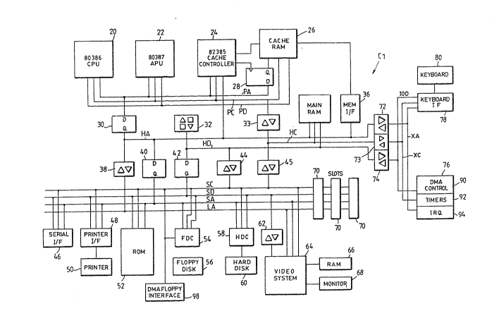
Referring now to Fig. 1, the letter Cl generally
: represents a computer based on the Industry Standard
; 5 Architecture inrorporating the first design according to
the present invention. A number of different blocks are
used in the computer ~1. The microprocessor 20 u ed is
preferably an 80386 microprocessor manufactured by Intel
Corporation (Intel). The microprocessor 20 has an addres~
bus PA, a data bus P~, and a control bus PC, these buses
PA, PD and PC being referred to as ~he local buses.
Coupled to the local bus are an arithmetic proces~ing ~nit.
or numerical coprocessor 22, preferably an 80387
~:manufactuxed by Intel; a cache controller 24, preferably
an ~2385 manufactured by Intel; cache RAM 26 and an
address latch 28. The cache controller 24 cooperates with
the cache RAM 26 to provide the necessary control to
handle a cache system in the computer Cl. The local bus
is connected to an intermediate ~us by means of a latch 30
which connects the local address bus P~ to an intermediate
address bus HA. A latched transceiver 32 connects the
local data bus PD to an intermediate data bus HD. A
transcei~er 33 connects the local control bus PC to an
intermediate control bus ~CO Connected to the
interme~iate bus is the main memory 34 in the computer C1
and a ~emory interface 36.
Variou~ other buses are developed from the
in~ermedia~e bus. For example, intermedia~e addre~s bus
~A is coupled by a transceiver 36 to an early ~ystem
address bus LA and by a latch 40 tQ a latched system
address bus SA. The intermediate data bus ED 1~ coupled
by a latch 42 a~d transceiver 44 to the ~y6tem data bus
SD. The intermediate control bus ~C is coupled by a
transceiver ~5 to the ~ystem control bus SC. Numerous
devic~s are coupled to the ~ystem buses LA, SA, SD, and SC
as are a ~eries of ~lots 70 which are used ~or receiving
interchangeable circuit bQard~ which contain additional
: . .
- --10 - ,
functions which can be utilized in the csmput~r Cl. A
~erial interface 46 is connected to the system data bus
SD, the latched system addrPss bus SA and the system
control hus SC. A printer interface 48 is also connected
to ~he æystem data bus SD, the latched system address bus
SA, and the system control bus SC, with a printer 50 being
attached to the printer interface 48. The read only
memory (ROM) 52 which contains the basic operating
software of the computer Cl is connected to the system
data bus SD, the latched system address bus SA, and the
system control bus SC. A floppy disk controller 54 is
connected to the system data bus SD, the latched system
address ~us SA, and the system control bus SC. A floppy
disk unit 56 which is used for providing storage for the
computer C1 is connected to the floppy disk controller 54.
A DMA-floppy control interface 98 is connected to the
system control bus SC and the floppy disk controller 54 to
intercept the TORC* signal and develop a new slgnal for
use by the ~loppy disk controller 54. A hard disk
controller 58 is connected to the system data bus SD, the
latched system addre~s bus SA, and the system control
bus S~ with a hard disk unit 60 being attached to th~ hard
disk controller 58. A video system 64 which controls the
presentation of data to the user i~ connected to the early
~y6tem address bus LA, ~he latched system address bus SA,
the ~ystem control bus SC, and coupled to the system data
bus S~ by means of a transceiver 62. Connected to the
Yideo system 64 are the random access memory (RAM) 66 used
to form the video memory and a monitor 6~ which presents
the desired display to the user. DMA~floppy interface
logic of ~he present invention is connected to the ~ystem
control bu~ SC and to the flsppy dis~ controller 54.
Various o~her subsystems are coupled to the
intermediate data, ~ddre~s ~nd control buses, XD, ~A and
HC, respectively. A tran~ceiver ~2 i6 connected to the
intermediate address bu6 ~A and to an e~tended address ~us
XA. A transc~iver 73 i8 connected to the intermediate
~ 7~
control bus ~C and to an extended control bus XC. A
transceiver 74 i~ con~ected between the intermediate data
bus ED and an input/output (I/O) data bus IOD. Connected
to the extended address bus XA, the data bus IOD, and the
extended control bus XC is a combined unit 76 which
contains the DMA controller 90 for the computer Cl, a
~eries o~ timers 92 and the interrupt controller 94. A
keyboard interface 78 is al~o connected to the ext~nded
address bus XA, the I/O data bus IOD and the extended
; 10 control bus XC. A keyboard 80 is connected to the
; keyboard interface 78 to allow the user to enter desired
character ~eguences and commands.
Familiarity with the signals forming the ISA is
assumed in this description. For more details on the ISA
signals and on the EISA signals, please reference the EISA
~pecification, Version 3.0 which is attached as Appendix
1. Generally, when referring to ~ignals in this
description, an asterik (*) following a signal mnemonic
indicates that it is logically true when a low voltage
level is pr~sent, and angle brach:ets with included numbers
after a ~ignal ~nemonic are used to indicate single or
multiple bit positions in a wider logical signal, such as
the D~A reguest lines. Additionally, in this dPscription,
the DMA requ~st line DRQ<2~ is generally referred to as
2~ the DREQ2 signal and the DMA a~nowledge signal DAK*<2> is
g~nerally re~erred t~ as the DAK2* signal for brevity.
The ~hannel two o~ ~he DMA channel-is conventionally used
for the floppy di~k controller in IBM PC compatible
computer ~y6temæ.
A brief summary o~ particular ISA signalc is of
intere~t. The BLCK ~ignal, the ~ynchronizing signal used
in the ystem ~ortio~ o~ the c~mputer ~ystem Cl operates
at a frequ~ncy between 8.333 MXæ and 6 MHz, has a nominal
duty cycl~ ~f 50~ and i6 driven only by the system board.
The AEN ~ignal i~ asserted (high) during DMA cycles to
prevent I/O ~laves from ~isinterpreting VMA cycles as
valid I/O cyclec. The ~EN* signal is an inverted version
- ~ , ,
.. . . .
12-- i " . ` s . 1 5~ ~`;,,
of the AEN signal. The IORC* signal is generally used to
indicate that an IfO device may drive data onto the bus,
this being the ca~e for the 82077. An ISA I/O device
generally drives data on the bus when the IORC* signal
and th~ AEN* signal axe simultaneously asserted. The
deYice generally must hold the data Yalid until sampling
the IORC* sign~l negated. ~owever, in some cases, such as
the 765 floppy disk controller circuits, the DAK* signal
is used in conjunction with the internal state of the
floppy disk controller to drive data onto the bus. The
MRDC* signal is asserted to indicat30 that the addressed
ISA memory slave hould drive its data onto the memory
bus.
The DRQ<x> lines are used by an I/O device to request
DMA service from the DMA sybsystem. The re~uesting device
generally holds the appropriate DRQ<x> lines asserted
until the system board asserts the appropriate DMA
acknowledge (DAK*<x>) signal. The DAK*<x> signals are
asserted by the DMA controller to indicate that a
particular channel has been granted the bus. For block or
demand mode DMA transfers, th~ DAK*<x> signal remains
asserted until the transfer completes or until the
centralized arbitration controller preempts the DMA
process. The T-C or terminal count signal is asserted by
~he D~A controller to indicate that a DMA chan~el's
transfer count has reached the terminal count. The DMA
controller asserts the T-C signal only while asserting the
channel's DAK*<~> signal. A DMA device decodes the T-C
~ignal wi~h the appropriate DAK*~x> signal asserted to
determine when the DMA transfer has been completed.
Referring now to Figure 2, the first design according
to3 the present invention is intended ~or ISAbased
computer~ and includes a programmable array logic (PAL)
device lV0 which includes a number of flip-flops and
utilizes cextain bus signals that are output from the DMA
controller 90 as well as an internally generated state
machine Ml (Figure 3) to generate a new version of the
: , ,; ., : :,~, , .:
,, .:: :. -: - .. :
.. ..
. 13
s ,,
IORC* ~ignal called NIORD* that i~ provided to the read or
RD* input 104 of ~he floppy disk controller 54. The bus
signals u~ed a~ inputs to the PAL 100 from the DMA
controller 90 includ~ the I~RC* signal; the MRDC* ~iqnal;
~he DAK2* signal; and the DREQ2 signal. The DCLK signal
is a version of the BCLK ~ignal that prferably has
one~half of the freguency of the BCLK signal.
The ADSTBO ~ignal is input to ~he P~L 100 directly
from the DMA controller 90. The ADSTBO signal is used to
load the multiplexed ei~ht higher or~er address bits from
the DMA controller 90 into a latch, from whlch they are
enabled onto the address bus ~hrough a three-state enable.
During block and demand transfer mode services, which
include multiple transfers, the addresses generated will
generally be sequential, and ~or ~any transfers the data
held in the external latch will remain the ~ame because
the upper eight address bits will remain the same. This
data need only change when a carry or borrow from A7 to A8
takes place in the ~ormal ~equence of addresses, and
therefore the DMA controller 90 updates ~he A8-A15 address
bits only as necessary. When this updating is necessary,
~he 8237 generally inserts extra ~tates ~o accomplish
this. The DCLK ignal is connected to the clock input o~
the PAL 100.
The PAL 100 uses these input signals to
generate an internal 3-bit ~tate machine Ml which is
clocked by the DCLK signal. Th~ different ~tates of the
state ~achine M1 are repre~ented by each o~ the bits Q0*,
Ql* and Q2*, which are represented as outputs ~rom the PAL
100 but are fed b~ck for use by the ne~t ~tate logic
contained in the PAL 100. The ~tate machine Ml
coordinates the proper generation of a ~iqnal called
CLKNIORD*, which i6 represented as an outpu~ of the PAL
100 and i~ asserted ~t $he appropriate time during a
35 veri:~y transfer. The CLKNIORD* ~iS~al and the IORC*
~ignal ar* combined in~ide the PAI 100 to produce the
NIORD* signal, which i~ output ~rom the lPAL 100 and is
cor~nected to the RD* input 104 of the floppy disk
-, .. , .. ; . ..... -:
-14-
controller 54, which controls the output of data from ~he
FIFO.
Referring now to Figure 3, the state machine Ml is
used to facilitate the proper generation of the CLKNIORD*
~ignal, which is uced to enable the proper assertion of
~he NIORD* ~ignal during verify transfers as demonstrated
in the timing diagrams of Figures 4, 5, 6 and 7. In the
tate eguations that follow, a particular ignal condition
is true when that sig~al is at a high state. The state
machine Ml transitions occur on the rising edge of the
DLCK ~ignal, which is provided to the clock inputs of the
flip-flops contained in ~he PAL 100.
State S0 is the initial state o the 6tate machine
Ml, and it also serves as the rest state of the state
machine Ml when no DMA transfers are taking place between
the floppy disk controller 54 and the DMA controller 90.
The ~tate machine Ml xemains in state S0 when the
equation:
(DAK2* x DREQ2*) I DAK2
is true. In other words, the state machine M1 remains in
its initial or rest state S0 Imtil the floppy disk
controller 54 issues a DMA re~uest. The state ~achine Ml
also remains in state S0 if the DAK2* signal is asserted
independently of the DREQ2 si~nal being asserted. The
state ~arhine M1 progresses from state S0 to state S1 when
the eguation:
DAK2* x DREQ2
is true. Therefore, the state machinP Ml undergoes a
transition from state SO to state Sl when a DMA re~uest,
~ignified by the assertion of th~ DREQ2 ~ignal, has been
made by the floppy controller 54.
The state machine ~1 remains in 6tate Sl while ~he
equation:
DREQ2 ~ ADSTBO*
i~ true. In st~te Sl, th~ state machine Ml is essentially
waiting or the ~DSTBO signal to be a~serted, ~ignifying
that the 8 higher order address bit~ are valid, before it
;, ~ ~ , " ,, ,:, :, ; , :
,., ,..:, . . .., : ,
: :: : !~' . .: . : :: ~ . . ' . .
--15--
~, is r.~
may continue. The state machine M1 returns to state S0 if
the eguation:
DREQ2* ~ ~DSTBO*
is true. Therefore, if the DREQ2 signal is negated before
~he ADSTBO signal is asserted, then the address is not
valid, and the state machine Ml returns to its S0 state.
If the ADSTBO signal i~ asserted before the DREQ2 ~ignal
i~ negated, a valid DMA transfer is occurring, and the
~tate machine Ml advances from ~tate Sl to state S2.
The state machine Ml returns to ~tate S0 from state
S2 if the DAK2* ~ignal is negated or raised to a high
level while the state machine M1 is in state S2. The
~tate machine Ml advances from state S2 to state S3 if the
eguation:
IORC* x DAK2 ~ MRDC*
is ~rue. This equation is generally only true during a
DMA verify cycle because, as shown in the timin~ diagr~ms,
a verify cycle is ~he only cyc:le where both the IORC*
~ignal and the MRDC* ~ignal are negated or high at this
time when ~he DAK2* signal is a.~serted. The IORC* and
MRDC* signals are both negated in a verify transfer
becauæe no actual transfer of clata occurs and the I/O
control lines are held inactive. Therefore, the state
~achine M1 advance~ from ~tate S2 to state S3 when a DMA
veri~y cycle is ~aking place. If either the IORC* ~ignal
or the MRDC* ~ignal are asserted in state S2 when the
DAX2* ~ignal i~ asserted, the~ a DMA write or DMA read,
respectively, i~ taking place, and the state ~achine Ml
advances from ~tate 52 to ~tate S4. Thi~ is evidenced by
the eguation:
(IORC ~ DAX2) + (M~DC x DAK2)
which advances the state ~achine M1 fro~ ~tate S2 to state
S4.
If ~he 6tate ~achine Ml has advanced to state S4,
then the cycle that is being executed is generally either
a DMA write or DMA read cycle, and, as ~hown in Figs. 4
and 5, ~t~te S4 i~ ~he state in which ~he actual transfer
-- . ~: . :, . . ~ . .
-16-
~! S, ` ,~ 1 . ,, rJ I,
of data occur~ The state m~chine Ml remain~ in state S4
while either the data transfer is still occurring,
signified by the DAX2* ~ignal remaining asserted, or, if
the DAX2* ~i~nal is negated, then the state machine Ml
remains in state S4 if a new data transfer is about to
take place, ~ignified by the DREQ2 sisnal being asserted.
Therefore, ~he state m~chine Ml generally remains in state
S4 while the equation:
(DAK2* ~ DREQ2) + DAK2
remains true, which is ~enerally until the data transfer
is completed. The ~tate machine Ml returns from state s4
to state S0 when ~he equation:
DAK2* x DREQ2*
is true, which signifies that the DMA read or write
transfer ha~ been completed.
If the state machine Ml has advanced to state S3,
~hen a DMA verify transfer is assumed to be taking place.
The state machine ~1 xeturns to state S0 from state S3 if
any of the conditions for a DMA verify transfer, namely
~he ~tatus of the signals in the equation ~hat advanced
the state machine Ml from state S2 to state S3, are not
met. ~or the state machine Ml to return from state S3 to
~tate S0, the eguation:
IORC ~ NRDC + DAK2*
25 DUSt be true. Th~refore, if either the IORC~ signal or
the MRDC* signal are as~erted in state S3, then a verify
transfar i~ not taki~ place and the state machine Ml
returns to state S0. A negation of the D~K2* signal in
~tate S3, possibly by the centrali7ed arbitration
controller (not shown) preemptlng the DMA process, also
~eturns the ~tat~ machine Ml to state S0. This eguation
i~ the oppo~ite of the equation:
IORC* x MRDC* ~ DAX2
which signified in ~tate S2 that a verify transfer was
occurri~g and was r~sponsible for advancing the stake
machine Ml from 6tate 52 to state S3 originally.
Therefore, if ~he eguation that is necessary for a valid
., ,, . . :..... . ~.... .
,: ,:
: . : : : ::
- . . ". ' ;' :. '~
,
-17-
r~ 7 ~
DMA verify transfer to be occuring is no longer true in
~tate S3, then it is assumed that either the verify
transfer i~ completed or that a valid DMA verify transfer
is not actually taking place, and the state machine Ml is
returned to ~tate 50. If the equation:
IO~C* x MRDC* x DAK2
~hat advanced ~he ~tate machine from state S2 to state S3
is ~till true in state S3, ~hen the state machine Ml
advances from state S3 to state S5 on the next rising edge
of the DCLK signal.
As shown in Figures 6 and 7, when the state machine
Ml has advanced to state S5, ~hen generally a verify cycle
has just occurred. The progression of the state machine
M1 after the S5 state depends on whether another verify
cycle is about to commence or whether the verify transfer
is completed. This is determined by the DREQ2 signal,
which is asserted if another verify cycle is to take place
and is negated if the verify transfer is completed. The
DREQ2 ~isnal is khe different component between the
equation:
IORC* ~ MR3C* x DAK2 x DREQ2
that progresses the state machine Ml from state S5 to
~tate S6, and the first Mintenm of the equation:
(~ORC* x ~DC* x DAK2 ~ DREQ2*) +
MRDC ~ IORC + DAR2*
which returns the ~tate machine Ml from state S5 to state
SO. I~ any of ~he last 3 minterms in ~he above equation
- that return~ ~he ~tate machine ~1 from state 55 to state
SO are tlue, ~hen a valid ~MA verify transfer is not
occurri~g and the ~tate machine Ml returns to state S0.
When the state machine Ml has advanced to state 56,
then it ~ay ~ither remain in ~tate S6, return to state S3,
dependent on ~he statu~ of the ADSTBO ~ignal, or return to
6tate S0 if ~he conditions of a ~MA verify tran~fer are
not ~et. The ~tat~ machine ~1 remains in state S6 when
~he eguation:
- : ~ :: ~ :. :
.. ~, . . : . ...
--18--
"; r~,
S.~ S ~
IORC* x M~DC~ x DAK2 x ADSTBO
is true, and ~he ~tate machine Ml progresses from state S6
to state S3 when the eguation:
IORC* x MRDC* x DA~2 x ADSTBO*
is true. In other words, if the conditions for a valid
verify cycle are met and the ADSTBO signal is asserted in
state S6, then the DMA controller 90 is updating the upper
8 bits in its address latch, and the state machine Ml
remains in state S6. As shown in Figure 7, if there are
multiple address strobes in the verify transfer, the
ADSTBO signal is asserted in state S6 and an extra S6
state is inserted in the progression of the state machine
Ml. If the ADSTBO signal is negated in state S6, then the
state machine M1 returns to states S3 in anticipation of
ano~her verify cycle. If the equation:
IORC + MRDC + DAK2*
is true in state S6, then a valid DMA verify transfer is
not actually taking place, and ~he state machine M1
returns from state S6 to state S0.
The state machine M1 and the above-mentioned bus
sig~al inputs are used to generate an output signal called
CLKNIORD*, the e~uation for which is:
CLKNIORD = (DAK2 x IORC* x NRDC* x S2)
(~DSTBO* ~ DAK2 x IORC* x MRDC x (S2 + S6))
The CLKNIORD* ~ignal is asserted at the appropriate time
during a DMA verify transfer between ~he floppy disk 54
controller and ~he DMA controller 90. As shown in the
first minterm of ~he above equation, the CLKNIORD* signal
is asserted in the ~tate following s*ate S2 if the
:: 30 conditions for a valid verify transfer, namely the DAK2
~ignal asserted and the IORC* and MRDC* signal negated,
are met. As ~hown in the second minterm of the above
eguation, the CLKNIORD* signal is asserted in ~he state
f~llowing either state S2 or tate S6 if the conditions
: : . ., , . ;: ... . ~ ,.:
, . , - ...... , ,: :.~. . .. .: :: - : :
: ~ :::: : ,, :::
. :: : : .. .,:,. : : . . ~::
:. :, :, : ; ~ ~
::: : :: ,: .,: ::: :, . : ::: : : :
--19--
f~ .3 7 ~
for a veri~y transfer are met and the ADSTBO signal is
negated.
The CLKNIORD* si~al is combined with the IORC*
signal from the bus to produce the NIORD* signal, the
~guation for which is:
NlORD = IORC + CLKNIORD
The PAL 10~ generally acts as an AND ~ate with the IORC*
signal and the CLKNIORD* signal as inputs and ~he NIORD*
signal as ~he output. Th~refore, the NIORD* signal is
asserted whenever ~he IORC* 6ignal i5 as~erted to maintain
the proper signal generation of the IORC* &ignal to the
floppy controller 54 during DMA read and DMA write
transfers. The NIORD* signal is also asserted at the
appropriate time during DMA verify cycles due to the
CLKNIORD* signal being asserted to provide clocking
signals to the floppy contxoller 54 to prevent FIFO
overrun.
Referring now to Figure 4, a timing diagram of a DMA
write cycle incorporating ~he present invention to the
floppy disk controller 54 is shown. In ~tate S0 the
floppy disk controller 54 m2~es ~1 DMA request by asserting
the DREQ2 signal, progressing the state machine M1 to
~ state Sl . This is followed by a DMA acknowledge (~AK2~
from the DMA con~roller coupled with the assertion of the
ADSTBO signal by the DMA controller to latch the upper 8
: address bits of the address destination, this causing the
~tate machine Ml to progress to state S2. While in ~tate
S2, ~he IORC* ~i~nal i6 a~iserted, ~igni~ying that the
floppy controller 54 may drive it~ data onto the bus and
~:; 30 progressing ~he ~ta~e ~achine ~1 to ~tate S4. The
assertion of the IORC* signal in Rtate S2 i~ responsible
for the basically ~imultaneou~ as~ertion of the NIO~D*
~ig~al. The ~RDC* signal i8 kept negated hi~h throughout
because thi i~ a DMA write ~ycle. In tate S4 the actual
transfer sf data takes pla~e rom the floppy controller 54
:~ to its memory destination and a~ ~any S4 ~tates as are
needed are in~rted here during thi~ data tran~fer. At
: ,: ,; . ,:: : . - .. , : . :
20-
~ome point during the transfer of data in state S4, the
DREQ2 signal is negated. When the data transfer is
~ompleted, the DAK2* signal is negated, causing the state
machine Ml to return ~rom state S4 to state S0.
Referring now to Figure 5, a DMA read cycle is shown
which is 6imilar to the DMA write cycle of Figure 4 except
~hat in this case the IORC* signal is negated (high)
~hroughout, causing the NIORD* signal to be 6imilarly
negated, and the MRDC* signal is asserted at the
appropriate times while the state machin~ Ml is in state
S4.
Referring now to Figure 6, a DMA verify cycle is
similar to the DMA write and read cycles of Figures 4 and
5, respectively, except that in this case both the IORC*
and MRDC* ~ignals are negated (high) throughout. ~owever,
the NIORD* signal is asserted at the appropxiate times in
state S3 o~ the ~tate machine Ml due to the CLKNIORD*
signal ~not shown) being asserted. Referring now to
Figure 7, a DMA verify cycle wit~ multlple address strobe
20 (ADSTB0) signals is similar to the DMA verify cycle of
Figure 6 exeept that the ~DSTBO signal is asserted a
~econd time in state S6. This results in an extra S6
state being inserted into the progression of the 6tate
machine M1, causing the subseguent assertion o~ the NIORD*
signal to be delayed 1 DCLK cycle.
The second design according to the presenk invention
is similar to the ~ir~t but is intende~ for use wi~h the
Ex~ended Indus~ry Standard Archi~ecture (EISA). Referring
now to Figures 8 and 9, the letter C2 designat~s generally
an EISA co~puter 6ystem inco~porating ~he present
invention. System C2 i~ compri~ed of a number of block
elements interconnected via four buses. For the sake o~
clarity, ~ystem C2 is 6hown in two portion~ with the
intercsnnections between Figures 8 and ~ desi~nated by
reference to the cirrled number~ one to eight. Many of
the d~tails o~ the portion of the system illustrated in
Figures 8 and 9 that are not discussed in detail below are
., . . -: .. ... -.. , : .. -
~, , ; , , .,, :. . ,,: ; . : .
: : ; . , .. :; ... .
:. .. , 1. . ..
: . . .:, . .~
-21-
not significant to the present invention other ~han to
illustrate an e~ample of a fully configured computer
system.
In Figure 8, a computer ~ystem C2 is depicted. A
S central processing unit CPU comprises a processor 220, a
numerical coprocessor Z22 and a cache memory controller
224 and associ~ted logic ~ircuits connected to a local
proce~sor bus 226. A~sociated with cache controller 224
is hi~h ~peed cache data random access memory 228,
noncacheable memory address map programming l~gic
circuitry 230, noncacheable address memory 232, address
e~change latch circuitry 234 and data exchange transceiver
236. A sociated wi~h ~he CPU also are local bus ready
loyic cirsuit 238, next address enable logic circuit 240
and bus request logic circuit 242.
In the drawings, system C2 is configured having the
processor bus 226, a host hus 244, an Extended Industry
Standard Architecture (EISA3 bus 246 (Fiy. 9) and an X bus
290. The EISA ~pecification Version 3.0 is included as
Appendix 1 to explain the reguir.ements of an EISA system.
The portion of system C2 illustrated in Fig. 9 is
essentially a configured EISA ~,ystem which includes the
necessary EISA bus 246, an EISA bus controller 248, data
latches and transceiver~ 250 and address latches and
; 25 buffers 252 to interface ~ekween the EISA bus 246 and the
host bus 244. Al~o illustraked in Figure 9 is an
integrated ~y~tem peripheral 254, which inco~porates a
~umber of the element~ u~ed in an EISA-ba~ed computer
~y~tem, among these a DMA controller 256.
The main memory array 253 is pre~erably dy~amic
random access memory. The memory 258 inter~ace~ with the
; host ~us 244 via a data buf~er circuit 260, a ~emory
controller circuit 262 a~d a memory mappi~g facility 268.
: The buffer 260 performs data transceiving and parity
generating and ch~cking functions.
The EISA bus 246 includes ISA and EISA con~r~l buses
276 and ~78, ISA and EISA data buses 280 and 282 and a
: ' ;. : : ::' : ~'' ,.' :.;,' '~ : . .: :,. :
-22-
~' b ~ rl ,~
~ystem address bus 284, a latched ISA address bus 286, and
a latched EISA address bus 288. System peripherals are
interfaced via the X bus 290 in combination with the ISA
control bus 276 from the EISA bus 246. Control and
data/addxess transfer for ~he X bus 290 are facilitated by
X bus control logic ~92, data transceivers 294 and address
buffers 296.
Attached to the X bus 290 are various peripheral
devices such as keyboard/mouse controller 29~ which
interfac~s the X bus 290 with a suitable keyboard and
mouse via connect~rs 300 and 302, respectively. Also
attached to the X bus 290 are read only memory circuits
306 which c~ntain basic operations software for the system
C2 and for system video operations. A serial
1~ communications port 308 is also connected to the system C2
via the X bus 290. Floppy and fixed disk 6upport, a
parallel port, a second serial port, and video support
circuits are provided in block circuit 310. A block
circuit 31~ generally containing various floppy disk
logic, including a floppy disk controller 318 (Fig. 10)
and a programmable array logic (PAL~ device 200 (Fig. 10)
that generates a ~ignal for ~he :Eloppy disk controller 318
according to the present invention, is also attached to
:~ the X bus 290. In this embodiment, the preferred floppy
disk controller 318 is ~he Intel 82077.
` Referrinq now to Figure 10, the second design
includes a programmable array logic (PAL) device 200 that
u~es certain ~ignal inputs from the computer system C2 as
well as a~ inte~n~l ~tate ~achine M2 (Fig. 11~ to generate
a new version of ~h~ IORC* ~ignal called FIORC* that is
pr~vide~ to the RD* input of the floppy disk controller
318. The bus ~ignals generally used as inputs to the PAL
209 fro~ the DMA contxoller 256 include the IORC* signal
and the AENO signal. The AENO signal i6 high duriny valid
I/O operations to the 6ystem board according to the EISA
~pecification. Other bu ~ignal inputs to the PAL 200
include the BCLR* signal, which is provided to flip-flops
--2 3 ~ d ~ .3
located in the PAL 200 and is used to advance the state
machine M2 and the T-C or terminal count signal. The
ST<2~ and ST<3> lines are output from the integrated
~y~tem peripheral (ISP~ 254 (Fig. 9~ and indicate, when
a6serted, that ~he DMA con~roller 256 is the current bus
master.
The PAL 200 uses *hese input signals to generate an
i~ternal 3~bit state machine M2. The different states of
the state machine M2 are represented by each of the bits
DQO, ~Ql, and DQ2 which are represented as outputs from
~he PAL 200. The state machi~e M2 utilizes the T-C signal
as well as the AEN ~ignal to coordinate the generation of
a new DMA terminal-count signal called DT-C, which is
represented as an output of the PAL 200. The state
machine M2 also coordinates the proper generation of a
6ignal call~d DFIOR*, which i6 output from the PAL 200 and
is asserted at the appropriate time during a DMA verify
transfer. The DFIOR~ signal and the IORC* are combined
inæide the logic of the PAL 200 to produce the FIORC*
signal, which is an output of the PAL 200 and is connected
to the ~D* input of the floppy disk controller 318.
Referring now to Figure 11, the state m~chine M2
generally include~ eight ~tate~, ætates O through 7,
through which it progressively counts upward~ The state
machine M2 is al~o rotational in that when it reaches
~tate 7 it retu~ns to state O and continues counting. The
. 6tate ~achine M2 generally remains in its ini~ial state of
ætate O until a I/O cycle i~ initiated aæ indicated by the
AENO* signal being assertsd. When the AENO* signal is
aæserted, a~ I/O cycle ha~ begun ~nd the 6tate machine M2
progr~sses fro~ state O to state 1. Thereafter, in order
for ~he state machine N2 to progress from ~tate 1 o~ward,
the AENO*, ST2, and ST3 si~nals must be a~serted. When
~he ~tatu~ bits ST2 and ST3 are asserted with the AENO*
6i~nal as~erted, then the cuxrent bus cycle is a DMA
cycle. Therefore, while a DMA cycl~ is in progress, the
state machi~e ~2 generally progres~es ~equentially from
-. ~ , . . ..
, " . , ! ,
', : . ' , ' ' ' ,' . ":
-24~
? " ~
state 0 to state 7 before returning to state 0 and then
repeating. The state machine M2 progresses through its
states while the AENO*, sr2, and ST3 signals are asserted,
and a negation of the AENO* signal returns the state
machine M2 to state 0 from any of the other states. A
negation of either of the ST2 or ST3 signals in states 1,
3 or 5 also returns the state machine M2 to ~tate 0. A
negation of ~he ST2 or ST3 si~nals in states 2, 4 or 6
returns the state machine M2 to state 1.
The P~L ~00 utilizes the ~tate machine M2 to aid in
the generation of of a new T-C or terminal count siynal
called DT-C, which is provided by a flip-flop in the PAL
200 clocked by the BCLK* signal, the equation of which is:
DT-C := (AENO x T-C x state 7)
+ (AENO x DT-C x (state 0 ~ state 1 ~ state
: 2 ~ state 3 + state 4 ~ state 5))
The PAL-generated DT-C signal is asserted when the state
machine M2 reaches ~tate 7 during a DMA cycle when the DMA
channel's w~rd count has ~eached terminal count as
indicated by the presence of the T-C ~ignal. The DT-C
signal remains asserted until ei.ther the AENO* signal is
` negated, which i~ when the DMA transfer is completed, or
until the state machine M2 has reached state 6, whichever
occurs first.
The PAL 200 utilizes the internally generated sta~e
. machine M2 states as well as the DT-C signal and various
other bus si~nals to ~enerate a signal called ~FIOR*,
which is provided by a flip-flop located in the PAL 200 ::
clocked by the ~CLK* ~ignal, ~he eguation of which is:
D~IOR := (AENO ~ state 3 x ST2 x ST3 ~ DT-C*)
~ I (AENO x DFIOR x (state 4 + state 5 ~ state
: 0 ~ ~tate 1~)
:~ The DFIOR* 6ignal is asserted at the appropriate time
:~ during verify cycles between the DMA controller 256 and
the floppy disk controllar 318. AS shown in the first
: minterm of the above equation, the DFIOR* 6i~nal is
. generally asserted during all DMA cycles on the falling
--25--
edge of the BCLK signal when the ~tate machine M2 is in
state 3, unless the DT-C signal i6 asserted. The DFIOR*
~ignal remain~ asserted until either the DMA cycle is
completed, siynified by the negation of the AEN* signal,
or until ~he ~tate machine M2 reaches ~tate 6, which ever
occurs first. Therefore, the DFIOR* ~i~nal is generally
asserted during 6tate~ 4, 5, 6 of the 6tate machine Ml
unless the ~ENO* signal is a6serted dusing this time.
The DFIOR* ~ignal is combined with the IORC* signal
10 to produce the FIORC* ~ignal, the equation for which is: ;
FIORC = IORC ~ DFIOR
The IORC* signal is included in the generation of the
FIORC* signal to ensure that the FIORC* 6ignal is as~ert2d
whenever the IORC* signal is asserted, this to maintain
the proper generation of the IORC* signal as supplied to
the ~loppy disk controller 31B during DMA read and DMA
write transfers.
Referring now to Figures 12, 13 and 1~, a:dem nd mode
verify cycle using the ISA compatible or normal cycle
control 6e~uence, a demand mode veri~y cycle using Type
"B" cycle control, and a demand mode verify cycle with
autoinitialize, respectively are shown. Each cycle begins
with the as~ertion of the ~ENO* ~ignal, which progresses
the ~tate machin~ M2 from ~tate 9 to state 1. The
~ssertion of the ~tatu~ lines ST<2,3~ in ~he beginning of
~tate 1 allows the ~tate machine M~ ~o continue counting
seguentially ~hxough its $tat~s as ~;hown. In each of
the~e demand verify cycles, the ~:NO*, ST2, and ST3
signal remain as~erted until ~everal ~tate~ after the DMA
30 terminal Cou21t (DT-C ) signal i~ asserted. The FIORC*
~ignal i8 a~serted once every 8 BCLK cycles wh~n the state
machine M2 is in ~tates 4, 5 and 6, this becau~e repeated
verify transfers during block or demand D~A requests
generally require 8 ~CLK cycles. In the dernand verify
35 cycle with autoinitialize or buffer chaining timing
diagram of Figure 14, th~ AENO* ~ al iB ~erted for
additional ~tates, as ar~ ~oth the T-C signal ~nd the DT-C
signal .
.
.. , . . , .. ,, - . . -
-26-
Re~erring ~ow to Figure 15, a single ~ode verify
cycle using type "B" cycle control is ~hown. The ~ingle
mode dictates that each cycle type is run as a ~ingle
Gycle transfer. Therefore, after the firct trans~er
cycle, where the FIORC* signal was asserted in states 4, 5
~nd 6, the i~ENO* signal is negated at the beginning of
6tate 2 following the first tran~fer cycle, effectively
~hort-circuiting ~he state machine M2 from state 2 to
state 0. The state machine M2 resumes counting from state
0 when the AENO* ~ignal is assert~d, and this cycle
repeats itself.
Therefore, two methods for generating a read FIFO
strobe pulse during DMA verify transfers are disclosed.
This prevents sverrun error~ that would occur in the FIFO
of the 8~077, allowing it to operating properly in FIFO
mode with older or noncompatible ~ystems coftware which
uses verify mode operations to determine floppy disk
transfer rates.
The foregoing disclosure and description of the
invention are illustrative and explanatory thereo~, and
various changes in the size, shape, materials, components,
circuit elements, wiring connect:ions and contacts, as well
as in the details of the illustrated circuitry and
construction and method of operation may be made wi~hout
~5 departing from ~he ~piri~ ~ the invention.
,''
" .
"
;
:
.: . , : , :,, ,, ;:, : :. , . , . - .
~: : : : . , . . - . . . ,. :, . : :. : . .. . . . . .