Note: Descriptions are shown in the official language in which they were submitted.
2~128r7 ~1~
-- 1
MULTILAYER CIRCUIT BOARD HAVING MIRCOPOROUS LAYERS
AND PROCESS FOR MAKING SAME
This application is a continuation-in-part of Lake
et al., U.5. Patent No. 4,915,983, entitled "Multilayer
Circuit Board Fabrication Process", assigned to the
assignee of the present application and incorporated by
reference herein in its entirety.
Back~round of the Invention
This invention relates to manufacturing printed
wiring boards and electrical components.
Printed wiring boards (PWB) perform several
indispensable functions in electronic devices of all
kinds. First, individual electrical components, e.g.,
specially packaged integrated circuits, resistors, etc.,
are mounted or carried on the surface of the flat,
usually sturdy, card-like board. Thus, the PWB serves as
a unitary mechanical support for the components.
Secondly, using chemically etched or plated conductor
patterns on the board's surface, the PWB forms the
desired electrical connections between the components.
Furthermore, the PW8 often includes metal areas serving
as heat sinks for high power or thermally sensitive
components.
As the use of integrated circuits has grown, the
higher density of connections between components has
necessitated double-sided PWB's in which additional
interconnections are made employing conductor patterns on
the other side of the board. This trend has been
extendad to boards having many layers of interconnections
called multilayer PWB's. Connections from layer to layer
are typically made by plated-through holes.
Conductor patterns can be formed using either
subtractive or additive processes. In a typical
subtractive proc~ss, a photoresist layer is applied to
.. .
.. . .
7 :~ Q
-- 2
the copper foil portion of a copper foil-clad epoxy
fiberylass substrate and patterned by exposure to
ultraviolet light through a stencil-like film artwork
mask. The exposed areas of the photoresist are
polymerized. The unexposed, unpolymeri~ed areas are
removed by a chemical developing solution, leaving areas
of copper having the desired conductor pattern underneath
the protective barrier of the remaining polymerized
photoresist. The exposed copper is then electroplated or
etched away (i.e. "subtracted") and the remaining
photoresist removed to expose the conductor pattern.
An additive process for forming the conductor
pattern starks with an insulating substrate, typically a
plastic laminate, throughout which is dispersed a
catalyst capable of initiatin~ metal plating on the
substrate; typical catalysts are palladium-based
materials. The catalytic substrate, referred to as a
1'fully additive base material," is coated with
photoresist and the photoresist is patterned as described
above. The holes through the resist formed when the
unpolymeriæed resist is washed away alre then filled with
metal using electroless plating techniques. Since the
conductors are produced by the addition of metal, rather
than subtraction as in etching, the process is called
"additive~l.
To promote adhesion betwean the plated metal and
the substrate, the substrate typically is coated with a
catalytic adhesive prior to application of the
photoresist. The adhesive is usually a resin blend
containing the plating catalyst and a colloidal
suspension o~ rubber. The adhesive is treated with a
strong etchant which primarily attacks the rubber
component, etching it almost entirely~ This treatment
creates catalytic micropores in the adhesive tha
8~:~Q
-- 3
promote adhesion between the plated metal and the
substrate surface.
In addition to the fully additive base material
described above, s~mi-additive base materials, which are
also adhesive-coated, can be used as the substrate
material. Both the semi-additive material and its
adhesive lack the dispersed catalyst. Th~y are rendered
microporous as described above and then immersed in a
solution containiny a precursor for the catalyst. The
precursor is subsequently activated to expose catalyic
sites for the plating operation.
Summary of the Invention
In general, the invention features in a first
aspect a composition of matter that includes a
catalytically seeded, photoprocessable, moderately
hydrophilic material. In preferred embodiments, the
wetting tension of the material (a measure of its
hydrophilicity/hydrophobicity) is at least 52 dynes/cm as
determined according to the method slet forth in ASTM
D2578-67. The preferred material includes an
ethylenically unsaturated monomer, a polymerization
initiator activatable by actinic radiation, at least one
preformed, water-soluble, polymeric binder, and a
particulate inorganic Eiller transparent to actinic
radiation (which preferably is bonded to the binder). It
is pre~erably seeded by coating the filler particles with
catalyst or by adding finely divided palladium or
palladium chloride catalyst seeds.
In a second aspect, the invention features a
printed wiring board that includes a circuit layer made
o a first material and a via layer made of a second
material different from the first material. In preferred
embodiments, the via layer i~cludes a cured microporous
photopolymer which is preferably moderately hydrophîlic
(with a wetting tension of at least 52 dynes/cm), e.g.,
.
. .
:
,,
~,
. . . .
_ 4 _ 2~2~7~
the polymerized product of an ethylenically unsaturated
monomer, a polymerization initiator activatable by
actinic radiation, at least one preEorm~d, water-soluble,
polymeric binder, and a particulate inorganic filler
transparent to actinic radiation in which the filler
particles are chemically bonded to the binder. The
micropores are preferably fractal micropores.
Another preferred via layer includes two layers of
a cured microporous photopolymer separated hy a layer of
woven fabric. The woven fabric preferably is capable of
bonding to the photopolymer and has a refractive index
that substantially matches the refractive index of the
photopolymer. The thickness of the upper layer of the
photopolymer preferably is less than the diameter of the
micropores.
The circuit layer of the printed wiring board
preferably includes a cured moderately hydrophobic
photopolymer whose wetting tension is less than 40
dynes/cm. The preferred photopolymer includes the
polymerized product of a monomer which is a half acryloyl
ester of bisphenol A epoxy monomer, a polymerization
initiator activata~le by actinic radiation, and at least
one preformed elastomeric polymeric binder that is
substantially free of acidic groups~ The photopolymer
preferably contains an acrylated urethane as wall.
In a third aspect, the invention faatures a
process for preparing the above-described printed wiring
board (as well as boards in which the via and circuit
layers ~re made of the same material) that includes the
steps of forming a microporous via layer from a
photoprocessable material; forming a circuit layer on the
via layer; and contacting the via and circuit layers with
a metal plating solution under reaction conditions
sufficient to deposit metal on the portions of the via
, ~ ' ' ::
~2~7~
-- 5 --
layer (but not the circuit layer) exposed to the plating
solution.
In preferred embodiments, the via layer is
mass-seeded with catalyst particles capable of initiating
metal plating prior to formation of the circuit layer or
selectively seeded with the catalyst particles subsequent
to formation of the circuit layer. Where the
photoprocessable material forming the via layer contains
filler particles, seeding may be accomplished by coating
the filler particles with catalyst prior to formation of
the micropores.
One preferred way of forming the micropores in the
via layer involves overlaying the photoprocessable
material with a mask having a plurality of dots, the
diameter of the dots being selected to create micropores
having a predetermined diameter; exposing the
photoprocessable material through the mask to a source of
radiation; and developing the exposed areas of the
photoprocessable material to create the micropores. The
dots preferably have diameters between 5 and 30 microns
and centers between 12 and 60 microns. The mask
preferably further includes a via pattern whereupon the
exposure and development steps simultaneously create vias
and micropores in the photoprocessable mat~rial.
A second preferred method for forming the
micropores involves preparing a digital repres~ntation of
a pattern that includes a plurality of dots, the diameter
of said dots being selected to create micropores having a
predetermined diameter; applying a layer of unexposed,
undeveloped photographic imaging film to thP
photoprocessable material that is sensitive to a
different spectrum of energy from the photoprocessable
material or is differentially sensitive to the same
spectrum of energy; selectively exposing the film with an
automatic photoplotter controlled by the digital
,
-- 6
representation to activate the film without affecting the
underlying layer of photoprocessable material; developing
the film; exposing the photoprocessable material through
the image developed in the film as an in situ mask; and
developing the exposed areas of the photoprocessable
material to create the micropores. As described above,
the diameter of each dot preferably is about 5 microns.
The pattern preferably further includes a via pattern so
that the imaging and development steps simultaneously
create vias and micropores in the photoprocessable
material.
In other preferred embodiments, the via layer is
treated with a reactive coupling agent to chemically bond
the agent to the surface of the via la~er. Examples of
preferred coupling agents include organotitanates,
organozirconates, and organosilanes, used alone or in
combination with each other. Preferably, the coupling
agent is capable of catalyzing the ~eposition of metal on
the exposed portions of the via layer.
In a fourth aspect, the invention features an
electroless plating process that includes contacting a
catalytically activated layer of a microporous
photoprocessable material deposited on a substrata with a
metal plating solution under reactic,n conditions
sufficient to deposit me~al on the portions of the layer
exposed to the plating solution.
In one preferred embodiment, the catalytically
activated layer is prepared by creating micropores in a
layer of photoprocessabl~ material deposited on a
substrate; curing the layer; and then seeding the layer
with a catalyst capable of initiating metal plating. In
another preferred embodiment, the catalytically
activated layer is prepared by incorporating a catalyst
in a photoprocessable material and then creating
micropores in the material. Preferred photoprocessable
' ' .
- 7 - ~ ~2
materials and methods for creating the micropores are as
described above.
In a fifth aspect, the invention features an
electroless plating process that includes the steps of
treating the surface of a photoprocessable material with
a reactive coupling agent to chemically bond the
photoprocessable material to the coupling agent; and
treating tha photoprocessable material with a metal
plating solution under reaction conditions sufficient to
depoit metal on the portions of the photoprocessable
material exposed to the plating solution. Preferred
coupling agents are as described above.
The invention also features a circuit component
(e.g., an inductor) fabricated from a microporous
photoprocessable material.
The invention provides printed wiring boards in
which metal plating adheres tenaciously and selectively
to the via layers and not in the circuit layer surfaces.
The use of a microporous photopro~essable material in the
via layers makes board manufacture simple and safe by
allowing metal to be plated directly onto the material
and by avoiding the need for special adhesives that must
be treated with strong, toxic, environmentally hazardous
etchants. Furthermore, multilayer boards can be
fabricated because theo6Xproblemef plating bath
contamination and etching of already plated metal
associated with the use of strong etchant~ are avoided.
Devices made of the microporous material are lightweight
and efficient.
Other features and advantages of the invention
will be apparent from the following description of the
pref~rred embodiments thereof~ and from the claims.
Description of the Preerred Embodiments
We first briefly describe the drawings.
,
,
-
,
2~7~
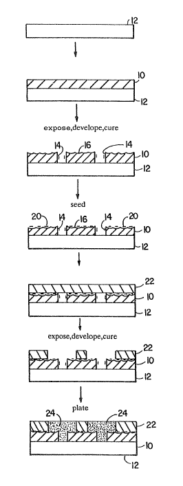
Fig. 1 is a diagrammatic cross-sectional view of
the sequential construction of a multilayer printed
wiring hoard fabricated using mass seeding.
Fig. 2 is a cross-sectional view of a fractal
micropore.
Fig. 3 is a diagrammatic cross-sectional view of
the sequential construction of a multilayer printed
wiring board ~abricated using selective seeding.
Fig. 4 is a cross-sectional view of a microporous
material having a woven mesh interposed between two
layers of photoprocessable material.
Detailed Description
Referring to Fig. 1, the first step in
constructing a representative single-sided printed wiring
board (PWB) using mass seeding is to hot-roller laminate
a layer 10 of photoprocessable material approximately
0.0015 inch thick on a copper plate 12 approximately
0.062 inch thick. The preferred photoprocessable
material is an aqueous-prOcessable, moderately
hydrophilic, dry film photopolymerizable composition as
disclosed in Tecle et al., European Patent Application
No. 87113013.4 published March 16, 1988 (hereby
incorporated by reference). This composition consists of
an ethylenically unsaturated monomer, an initiator
activatable by actinic radiation, at least one preformed,
water-soluble, polymeric binder, and particles of an
inor~anic material transparent to actinic radiation which
are chemically bonded to the binder. It has a wetting
t~nsion of at least 52 dynes/cm (e.g., 52-56 dynes/cm) as
measured according to ASTM D2578-67. The wetting tension
i5 an indication of the hydrophilicity/hydrophobicity of
the material; the higher the wetting tension the more
hydrophilic the material is.
As disclosed in Tecle ~t al., pre~erred ~illers
are silica, silicate, alumina, or carbonate particles (or
., , . . :
~Q~7~
g
derivatives thereof) in which at least 95% of the
particles have diameters between o.l and 15 microns.
Preferred binders include Carboset 525
(methylmethacrylate/ethyl acrylate/-acrylic acid),
Blendex 491, Lucite 47 KNL, Amphomer amphoteric
pentapolymer (tert-octyl-acrylamide/methyl
methacrylate/-hydroxypropyl-methacrylate/
tertbutylaminoethyl methacrylate/acrylic acid) acrylic
binder, and PVP K-90 (polyvinylpyrrolidone). Examples of
preferred monomers include acrylate, diacrylate, and
triacrylate monomers, e.g., pentaerythritol triacrylate
and trimethylol propane triacrylats, which may be used
alone or in combination with each other. Preferred
initiators are free radical generating addition
polymeriæation initiators activatable by actinic light,
e.g., benzophenone, Michler's ketone, diethyl
hydroxylamine, and 3-mercapto-1,2,4-triazole.
A series of vias and micropores is formed in layer
10 using the methods described in Lake et al., U.S.
Patent No. 4,666,818 entitled "Method of Patterning
Resist", assigned to the assignee of the present
application and incorporated by reference in its
entirety. According to these imaging methods, a thin,
unexposed, undeveloped strip base silver or other
photoimageable film (not shown) is placed over layer 10.
This ~ilm and layer 10 are either sensitive to different
energy spectra or show di~ferential sensitivity to a
single spectrum such that exposure of one does not affect
the other. The film is then exposed using a white light
x-y photoplotter driven by a computer aided design (CAD)
system to create a pattern of vias for ground picX-up
(the diameter of each via being approximately 0.005 inch)
and an entire field of small dots for creating
micropores. The actual dot pattern (and thus the
micropore pattern) is selected based upon the minimum
:
:, ' .
Pi ~ ~
-- 10 --
feature size to be anchored. For lines of 25 microns or
greater, the diameter of sach dot is between 5 and 30
microns and the dots are regularly spaced on
approximately 12-60 micron centers. The exposed film is
then developed to expose areas of layer 10 according to
the above-described pattern. These areas are then
exposed to ultraviolet (U.V.) light (approximately 150
millijoules/cm2 at 365 nm). Following U.V. exposure, the
film is peeled off and layer 10 is spray developed in a
1~ sodium carbonate monohydrate solution at 40C or a
0.75% monoethanolamine solution at 30C for about 1
minute, water rinsed, and dried.
The resulting layer has a series of completely
washed out via holes 14 extending down to copper ground
plane support 12. It also exhibits a series of
micropores 16 corresponding to areas of layer 10 exposed
through the dots in the film. Each micropore is washed
out to a depth of about 5-6 microns. Within each
micropore, there exists a series of secondary micropores
18 (Fig. 2) formed when unreacted photopolymer washes out
and filler particles remain in the walls of the micropore
during development; the resulting "micropore within a
micropore" structure is referred to as a fractal
micropore~ The micropore structure is also a result of
light scattering during exposure. The top and inner
surfaces of these micropores have a fine, matte surface
for anchoring catalytic plating seeds and plated metal to
layer 12.
Following development, lay~r 10 is exposed to U.VO
at 0.5 joulesfcm~ and then baXed at 300F for 1 hour,
followed by a second U.V. exposure at 4-5 joules/cm2. It
has been found that this cure process retains micropore
integrity more effectively than a full U.V. cure followed
by baking (which causes embrittlement~ or baking prior to
any U.V. exposure (which causes the resist to flow and
::
.. :: - :
7 ~ ~
fill the micropores). The composite structure formed by
layers 10 and 12 is then immersed in a series of
conventional cleaning and catalyst seeding solutions,
rinsed, and dried to deposit catalytic seeds 20 for
plating in the micropores.
~ ext, circuit layer 22 is created by hot roller
laminating a layer of a moderately hydrophobic
photoprocessable dry film. The preferred material is
disclosed in Gervay, European Patent Application No.
87117547.7 published June 15, 1988 (hereby incorporated
by reference) and consists of a monomer which is a half
acryloyl ester of bisphenol A epoxy monomer, a
polymerization initiator activatable by actinic
radiation, and at least one preformed elastomeric
polymeric binder that is substantially free of acidic
groups ~e.g., the number of acidic groups is sufficiently
low such that the composition can withstand contact for
24 hours to a liquid at a pH of 12 maintained at a
temperature of 70C; an example of such a liquid is an
electroless plating bath liquid composition described on
page 7-6 of "Printed Circuits Handbook" Second Edition,
ed. by Clyde F. Coombs, Jr., McGraw-Hill Book Co., 1979).
It may also include an acrylated urethane, as well as
dyes, pigments, fillers, and thermal polymerization
inhibitors. It has a wetting tension of less than 40
dynes~cm ~e.g., between 35-40 dynes/cm3.
As disclosed in Gervay, preferred monomers have
the formula
~ ~ ~ , ~` ~a
S~
where Rl is -(CH2)~-CH-CH2,
R2 is -A-C-C=C~2,
12 ~2$71~
.
R3 is H or an alkyl group having between 1 and 10
carbon atoms, inclusive,
A is [~(CH~)q~0~~]~ or
Of ~r
-(Ch2-CH-CH2-0)~ or
5 0 R3 -A- represents a linkage between 0 and
-C-C-~=CH2, and
m, q, r, and s, independently, are int~gers from 1
to 10 and n is zero or an integer from 1 to 5.
Preferred bindars include the elastomers described
on page 232 of "Hackh's Chemical Dictionary" Fourth
Edition, ed. by J. Grant, McGraw-Hill Book Co. 1972~ The
binders are water-insoluble, e.g., they will not dissolve
in water at room temperature during 4 hours. Examples of
preferred binders include methylmethacrylate/
butadiene/styrene terpolymer ~e.g., Acryloid BTA-IIIs
and BTA-IIIN2 commercially available from Rohm and Haas).
Preferred initiators are free radical generating addition
polymerization initiators activatable by actinic light,
e.g., benzophenone, Michler's ketone, diethyl
hydroxylamine, and 3-mercapto-1,2,4-t:riazole. Preferred
urethanes include conventional, commercially available
products such as CMD-6700, Chempol-1'3-4827, and
Gafguard-23~ present in an amount of 0 ~o 30 parts by
weight.
The thickness of layer 22 is about 0.0012 inch. ;~
Layer 22 is overlaid with a mask having the desired
circuit and ground pick-up pattern, exposed to
approximately 250 millijoulesfcm2 o~ U.V. light through
the mask, and developed in 1,1,1 - trichloroethane for
about 1 minute at 25C. Following devalopment, the
circuit pattern washes out completely down to the seeded
microporous layer. Next, layer 22 is baked at 300F for
.
^.
?
2~ 7~ ~
- 13 -
circuit pattern washes out completely down to the seeded
microporous layer. Next, layer 22 is baked at 300F for
30 minutes, followed by flood exposure to U.V. light (2.5
joule/cm2 at 365 nm) to fully cure it.
Following cure, the prepared substrate is
chemically cleaned and then strike plated in a
conventional electroless copper plating bath of the type
commonly used for depositing copper in plated through
holes. After about 40-80 microinches of copper have been
deposited on microporous layer 10 and in the vias, the
substrate is removed from the bath and transferred to a
full build, high guality electroless copper plating bath
of the type commonly used for fully additive plating of
printed circuit boards. When the resulting electroless
copper deposit 24 has plated flush to the surface of
circuit layer 22, the substrate is removed from the
plating bath. Vias from the ground plane layer 12 are
formed and connected to circuit layer 22, as defined by
the circuit pattern.
The above-described process is repeated as many
times as necessary to create a printed wiring~86Xboard
having the desired number of circuit and via layers.
The second circuit layer Will interconnect to the first
circuit layer through vias washed out of the microporous
Vacrel layer down to copper metal sites on the first
circuît layer according to the circuit pattern.
Fig. 3 illustrates the preparation of a
multilayered printed wiring board using selective
seeding. In this process, the catalyst seeds are added
separately, rather than forming an integral part of the
insulating substrate. An advantage of selective seeding
is improved retention of the substrate's insulating
properties upon exposure to conditions of high
t~mperature and humidity because conductive anodic
filamentation is minimized.
.
~` ,.
7~
~ 14 -
Referring to Fig. 3, a 0.030 inch glass-epoxy
unclad type FR-4 substrate 26 is drilled for plated
through hole interconnects 28. The drilled holes have
diameters between 0.007 and 0.015 inch. Substrate 2~ is
then cleaned, surface-prepped, and hot roller laminated
on both sides with a photopolymer 30 having the
composition disclosed in Tecle et al. described earlier
for the mass seeding case (each layer being about 0.0015
inch thick).
Next, each photopolymar layer is overlaid with a
thin silver or other photo-imageable film (not shown) as
described above for the mass seeding process and the film
exposed with the CAD~driven photoplotter and then
developed to create a pad pattern identical to the
drilled hole pattern and an entire field of small dots,
each about 0.0002 inch (5 microns) in diameter spaced on
approximately 0.0005 inch (12 microns) centers. The
photopolvmer layers are then exposed through the films to
U.V. light (about 150 millijoules/cm2 at a wavelength of
365 nm). Following removal of the films, the
photopolymer layers are spray-develc,ped in a ~% sodium
carbonate monohydrate solution at 40C or 0.75%
monoethanolamine solution at 30C fc,r about one minute,
rinsed with water, and dried. The resulting microporous
surfaces have completely washed out via holes
superimposed over the drilled holes in the substrate with
the 5-30 micron diameter micropores 32 washed out to a
depth of about 5-6 microns. The top and inner surfaces
of the washed out micropores have a fine matte surface
because these micropores are fractal micropores, as
described above for the mass seeded process. The
photopolymer layers are then exposed to U.V. at 0.5
~oules/cm2, baked at 300F for 1 hour, and then exposed
to U.V. at 4-5 joules/cm2.
.
~3~
~ lS
The next step is to hot roller laminate each
photopolymer layer with a 0.0012 inch thick layer 34 of
the moderately hydrophobic photopolymer disclosed in
Gervay and described earlier for the mass seeding case.
These layers are then overlaid with masks having the
desired circuit and via pickup patterns for each side,
exposed to about 250 millijoules/cm2 of U.V. light at 365
nm through the masks, and spray developed in
1,1,1-trichloroethane for about one minute at 25C. Upon
development, the desired circuit and via pickup patterns
wash out completely down to the microporous surfaces.
The substrate is then baked at 300~F for 30 minutes
followed by flood exposure to U.V. light (2.5 joules/cm2
at 365 r.m) on both sides.
Following the U.V. flood exposure, the substrate
is immersed in a series of cleaning and catalysing
solutions to deposit catalytic seeds 35 for initiating
metal plating in the micropores. Catalyst is selectively
deposited in the micropores due to the hydrophilic nature
o~ the via layer (to which the seeding solution is
attracted) and the hydrophobic nature of the circuit
layer (which repels the seeding solution). The
selectively seeded substrate is then rinsed and immersed
in an ele&troless copper strike bath of the type commonly
used for copper deposition in plated through holes.
After approximately 40-80 micro-inches of copper is
plated in the through holes and exposed microporous
surfaces, the substrate is removed and transferred to a
high quality, full build electroless copper plating bath
of the type commonly used for fully additive plating of
printed circuit boards. The substrate is removed when
the copper is plated flush to the surfaces of the
moderately hydrophobic photopolymer.
The above-described process is repeated as many
times as necessary to create a printed wiring board
. ~ : .
:
~2~
- 16 -
having the desired number of circuit and via layers.
The outer circuit layers will interconnect to the inner
circuit layers through vias washed out of the microporous
Vacrel layers according to the circuit pattern.
Other embodiments are within the following claims.
For example, referring to Fig. 4, a finely woven
cloth 36 (e.g., made of fiberglass) may be inserted
between two layers of photopolymer (e.g., the moderately
hydrophilic photopolymer of Tecle et al.) 38, 40. During
processing, the weave is uncovered, thereby providing
discrete reinforcement and a uniform number of locking
bond sites for anchoring catalyst seeds to ensure uniform
adhesion of metal plating no matter where holes are
photoformed and filled with metal. The weave also helps
control thermal expansion, thus making the board more
failure resistant. Preferably, the weave is made of a
bondable material having a refractive index matching that
of the photopolymer to minimize bloom ~nd scattering.
The top photopolymer layer 38 preferably is thinner than
the diameter of the micropore 42 formed upon U.V.
exposure and development so that the pores will fully
wash out when processed. This ensures that the cross
weave bonding sites are properly exposed for plating.
The surface of the woven fabric can also be
pre-treated with a reducing agent, e.g., palladium
chloride or colloidal palladium solutions, prior to
insertion between the photopolymer layers. This would
auto-catalyze the platin~ process and ensure an excellent
bond between the plated metal and the photopolymer layer.
Instead of using mass seeding or selective seeding
techniques, the filler particles of the microporous
photoprocessable material can be coated with catalyst
during initial fabrication of the photoprocessable
material prior to micropore formation.
,
.
l Q
- 17 -
Micropores and vias can be formed in the
photoprocessable material by exposing the material
through a mask having a pattern of vias and holes for
forming the micropores, rather than using the
CAD-directed photoplotter in combination with the thin
silver film. Similarly, the circuit layer can be imaged
using the CAD-directed photoplotter in combination with
the thin silver film, rather than a mask.
Circuit components such as inductors can be
prepared from the microporous material using the methods
described in Williams, U.S. Patent No. 4,873,757 entitled
"Multilayer Electrical Coil" which is assigned to the
same assignee as the present application and hereby
incorporated by reference in its entirety.
Adhesion of plated metal to the via layer (which
may or may not be microporous) can also be promoted by
treating the surface of the layer with a reactive
coupling agent prior to final cure, e.g., by using the
agent as the developing solution or by immersing the via
layer in a water solution o~ the agent after development,
followed by a rinse. The subsequent U.V. and thermal
cure chemically bonds the agent to the surface, where it
can then act to promote adhesion of subsequently plated
metal. The coupling agent may also act as a catalyst for
metal plating at the same time. Exalmples of suitable
coupling agents include organotitanates (e.g., titanium
triethanolamine and diethanolamine commercially available
from DuPont as Tyzor TE and Tyzor DEA, respectively),
organozirconates (e.g., zirconium ethylene diamine
commercially available from DuPont as Tyzor 212~, an~
organosilanes (e.g., methacryloxypropyltrimethoxysilane
and aminopropyltriethoxysilane, both of which are
commercially available from Petrarch Chemicals as
Petrarch M8550 and AP750, respectively).
. ~ .