Note: Descriptions are shown in the official language in which they were submitted.
202880~ - ~
. . .
The present invention relates to a compound
semiconductor epitaxial wafer in which ia heteroepitaxial
crystal layer is formed above a compound semiconductor single
crystal substrate.
An optical element such as a light emitting element
or a photoreceptor has a structure obtained by skilfully
combining regions which have different optical and electrical
properties. In addition, the production necessarily takes
place by an epitaxial technique since such a structure must
be formed by a single layer of crystals on a base of already
completed crystals. Epitaxial crystals are classified into
homoepitaxial crystals and heteroepitaxial crystals, depending
on whether a substrate and an epitaxial layer formed on the
substrate are of the same material or of different materials,
respectively.
In a conventional compound semiconductor
heteroepitaxial wafer, upper, lower, left and right portions
of a substrate having a diameter of two inches, for example,
are cut-off to shape the substrate into a rectangular
configuration and thereafter an epitaxial growth is caused on
the rectangular substrate by a liquid phase growth method or
a vapor phase growth method. These methods take into
consideration the technical restriction of an epitaxial growth
on the compound semiconductor substrate.
However, such a conventional rectangular epitaxial
wafer has had the following problems. One problem is the fact
that the thickness of a resist film applied by spin coating
or the like, is heterogenized at corner portions of the outer
periphery in a pattern formation such as photolithography
whereby a good pattern formation cannot be achieved in these
corner portions and the yield is reduced. Another problem is
the fact that the corner portions tend to crack or chip in
response to physical impact or the like. Hence, the
manufacturing yield is reduced.
In order to overcome such problems, it is possible
to use an epitaxial wafer having a circular configuration.
.;`'~. `~ ' '
~S ~ ~
, .
. .. ~ , .
;~.
. .
2 0 2 8 8 0 8
In fact, a high yield has been obtained by employing a
circular substrate for silicon semiconductors. However, the
present inventors have found that a high yield cannot be
achieved by directly employing a compound semiconductor
heteroepitaxial wafer having a circular configuration. This
finding is contrary to what is known regarding silicon i~;~
semiconductors, as will now be described.
In a compound semiconductor, it is difficult to grow
single crystals while maintaining a uniform stoichiometric ~ -
composition, as compared with growth of crystals of a simple
substance such as silicon. Thus, bulk crystals of a compound -
semiconductor are generally inferior in their uniformity
compared to silicon semiconductors. The defects of a circular -~
compound semiconductor substrate tend to be concentrated in
its outer periphery, and the defects propagate toward an
epitaxial crystal layer if epitaxial growth is caused on this ~ ;
peripheral portion. It has been recognized that the defects
of the outer peripheral portion, particularly slip defects
propagate and extend toward a wafer center portion, which
initially is absolutely nondefective in itself. This
propagation after epitaxial growth is due to thermal stress
and physical stress during processing of a semiconductor
device. A detailed description of slip defects is provided
in J. Appl. Phys. 54(2), February 1983, p. 666 - 672, for
example. The definition of slip defects is directed to at
least ten crystal defects aligning on a straight line of 1 mm.
According to the present invention, there is
provided a compound semiconductor epitaxial wafer, comprising
a compound semiconductor single crystal substrate having a
30 substantially circular configuration, a heteroepitaxial -~
crystal layer formed on said compound semiconductor single
crystal substrate, means for preventing propagation of ~ .
defects, said defects propagation preventing means forming
part of said wafer and extending into said substrate to
surround an area of said wafer prior to wafer processing so
that defects starting outside said area of said wafer during
.
.
.~. . ~ :,
!.'\ . ",~.. , . : , ' : ~: ':
2 0 2 8 8 0 8
wafer processing cannot propagate into said area surrounded
by said defects propagation preventing means;during said wafer -I
processing, and wherein said compound semiconductor single
crystal substrate is free of dislocation defects at least
within said area surrounded by said defects propagation
preventing means.
According to another aspect of the present i
Iinvention, there is provided a compound semiconductor
epitaxial wafer, comprising a compound semiconductor single
crystal substrate, a heteroepitaxial crystal layer formed on
said substrate, said substrate comprising a central area which
is free of dislocation defects, said compound semiconductor
epitaxial wafer further comprising, as part of said wafer,
means extending into said substrate for cutting of a linkage
between a crystal portion in said central area of said
substrate from a crystal portion outside said central area of
said substrate, said cutting off means extending through said
heteroepitaxial crystal layer and into said substrate prior
to wafer processing, whereby said cutting off means suppresses
propagation of crystal defects to said area free of
dislocation defects during said processing of said wafer.
The present invention, enables the provision of a
heteroepitaxial crystal wafer which will not transfer large
Ilcrystal defects to a heteroepitaxial crystal layer formed on
i25 a substrate over the entire surface whereby the compound
semiconductor substrate is dislocation free. Further, since ~ -
the compound semiconductor substrate has a substantially
circular configuration, it is possible to remarkably increase
the production yield without causing heterogeneity of a resist
film, which has been observed in the case of employing a
Iconventional rectangular substrate. In addition, it is now
possible to obtain a device which has excellent
characteristics over the entire region of a circular
configuration without causing new crystal defects by thermal
stress and physical stress caused by an external force applied
~ ~ .
~ . .
.
2 0 2 8 8 0 8
in an intermediate stage of processing. Any propagation of :: ~ -
crystal defects is also prevented.
When a compound semiconductor substrate still having
crystal defects is employed, a similar effect can be attained
by cutting off a linkage in a heteroepitaxial layer so that
no bad influence is exerted by existing crystal defects.
Figures 1 to 3 are Eront elevational views for
illustrating a method of growing an epitaxial layer on a
dislocation ~ree circular substrate according to the present
invention;
Figure l is a front elevational view showing a
substrate obtained by slicing an ingot;
Figure 2 is a front elevational view showing an
epitaxial wafer after heteroepitaxial growth;
15Figure 3 is a front elevational view showing the
substrate after pattern formation working;
Figures 4 to 6 are front elevational views
illustrating conventional methods of growing an epitaxial
layer on a rectangular substrate;
20Figure 4 is a front elevational view showing a
substrate obtained by slicing an ingot;
Figure 5 is a front elevational view showing an
epitaxial wafer heteroepitaxially grown on a rectangular ;~:
portion cut out along broken lines in Figure 4;
25Figure 6 is a front elevational view showing the
substrate after pattern formation working;
Figures 7 and 8 are front elevational views
illustrating a conventional comparative method of growing an
epitaxial layer on a circular substrate which is not ~
30 dislocation free; - ~-
Figure 7 is a front elevational view showing a
substrate obtained by slicing an ingot, whereby an epitaxial
wafer after heteroepitaxial growth is similar to the state
sho~n;
35Figure 8 is a front elevational view showing the ~-
substrate after pattern formation working; ~
~. ~
2028808
: ,
Figures 9 to 14 are plan views showing the
propagation of defects due to working of an epitaxial wafer
obtained by growing a heteroepitaxial crystal growth layer on
~` a compound semiconductor; ~ ~
. 5 Figure 9 is a plan view showing a wafer obtainad ~ -
: after growing heteroepitaxial crystal layer above a compound
; semiconductor single crystal substrate; ~:
dFigure 10 is a plan view showing a wafer after
~, processing the semiconductor wafer of Figure 9 by a ~
:10 conventional method; ~:
Figure 11 is a plan view showing the wafer which is :~ ;
provided in its outer peripheral portion with means for :
cutting off a linkage between crystals in the heteroepitaxial
:; crystal layer of the wafer shown in Figure 9; ~ ~:
, 15 Figure 12 is a plan view showing a wafer which is . :
:~ provided with the means for cutting off- a linkage between
crystals in the heteroepitaxial crystal layer of the wafer
shown in Figure 9 in the form of a lattice for en~losing every
element; -
Figure 13 shows trenches as an example of a cut-off
si device; ~ .
Figure 14 is a plan view showing the outer
peripheral portion of a wafer which includes defects;
Figures 15 to 18 are sectional views showing the
propagation of a crystal defect as a result of processing of
~ an epitaxial wafer; -~
d Figure 15 is a sectional view showing one typical
crystal defect of defects that may be present in the wafer of ~- ::
.~ Figure 9;
Figure 16 is a sectional view showing propagation
. of the crystal defect to the epitaxial crystal layer in the :-
wafer of Figure 10;
Figure 17 is a sectional view showing a section
~1 through the wafer of Figure 13; -:
-~
,~ .
". : ::. :- ~ '
2028~08 : ~ :
Figure 18 is a sectional view showing a state of
propagation of the crystal defect in the epitaxial layer after
processing the wafer of Figure 17.
A compound semiconductor epitaxial wafer according
to the present invention is a compound semiconductor single
crystal substrate of substantially circular configuration and
having formed thereon a heteroepitaxial crystal layer which
is free of any dislocation.
In a method of improving heterogeneity of a resist
film formed by spin coating, it may be relatively easy to
employ a substrate having a substantially circular
configuration in place of the conventional rectangular
substrate. However, the present invention is specifically
directed to a substrate having a substantially circular
configuration, which is dislocation free for use as a
substrate for forming an epitaxial crystal layer.
It has been found according to the invention that
the yield cannot be improved in the case of employing a
substrate, which has a substantially circular configuration
but is not dislocation free, as is used in general. The term
dislocation free means a state including no slips (linear
defects) with EPD (etch pit density; crystal defect density)
of not more than 500tcm2. A slip is defined as at least ten
crystal defects aligned on a straight line of 1 mm as
described in more detail in the aforementioned literature.
The present invention improves the heterogeneity
caused by spin coating thereby also improving the yield by
employing a substrate having a substantially circular
configuration, as well as preventing reduction of the yield
by the propagation of defects, particularly slips, by
employing a dislocation free substrate.
Figures 4 to 6 are front elevational views for
illustrating a conventional method of growing an epitaxial
crystal layer on a rectangular substrate.
Figure 4 is a front elevational view showing a
substrate 1 which is obtained by slicing a compound
- ~ ' . -
.,,,,:
~. . .. ~ . ,
;, .. .. . .
2028808
semiconductor single crystal ingot, for example an InP singlecrystal ingot. The substrate plane of a circular InP single
crystal substrate 1 is the ~100) plane. The cleavable
directions of the single crystal substrate are [011] and a
direction perpendicular thereto. The circular InP single
crystal substrate 1 is a generally used InP single crystal
substrate which has a portion of considerable crystal defects
and slips. This portion exists in the outer peripheral area
along the [001] direction and in the direction perpendicular
thereto. A dislocation free portion or area is surrounded by
the curved line in Figure 4. Inside the dislocation free
portion 2~ the upper, lower, left and right sections are cut-
off as shown by dotted lines in Figure 4, to make a
rectangular substrate 3. Epitaxial growth is caused on this
rectangular substrate 3. Therefore, substantially no slips
have existed in the conventional rectangular substrate 3.
Figure 5 is a front elevational view showing the
substrate 3 after heteroepitaxial growth. Referring to Figure
5, an available effective portion is shown with hatching. In
other words, the entire rectangular wafer 3 is substantially
effective. Then a resist film is applied onto this
rectangular wafer 3 by spin coating or the like, to perform
a pattern formation working.
Figure 6 is a front elevational view showing the
substrate after the pattern has been formed. Referring to
Figure 6, an effective portion 5 is shown with hatching and
corner portions 4 of the rectangular wafer 3 define a
heterogeneous resist portion 4, whereby the available portion
is further reduced with a respective reduction in the yield.
Figures 7 and 8 are front elevational views
illustrating a method of growing an epitaxial layex on a
circular substrate which is not dislocation free.
Figure 7 is a front elevational view showing a
substrate 1 which is obtained by slicing an ingot, similarly
to the substrate 1 shown in Figure 4. In this case, the
substrate 1 is not rectangularly cut out but heteroepitaxial
'
R~
., ~_
,, , ; . . , . ~ . . ~ . . ~. . -
. -
. , .
. ~
:
'' ~' . . ' ''
,. - : .
` 2028808 ::~.
growth is directly made on the circular substrate 1. The
`~ state of the epitaxial wafer after heteroepitaxial growth is
similar to that of Figure 7 since it directly receives crystal
defects of the substrate.
Figure 8 is a front elevational view showing the
substrate 1 after pattern formation working has been
completed. The portion with hatching shows the effective
portion 7. Thus, slips in the outer peripheral portion of a
circular InP single crystal substrate 1 are inwardly
propagated by stress occurring when the device is processed,
and hence the dislocation free portion or area 7 is reduced.
Thus, when a epitaxial wafer provided on a circular
substrate which is not dislocation free is exposecl to
processing steps, slips inevitably reach a portion, which has
been dislocation free, after heteroepitaxial growth, and an
effective portion or area is rather reduced to lower the
yield.
Figures 1 to 3 are front elevational views for
illustrating a method of growing an epitaxial layer on a
dislocation free circular substrate in accordance with the
present invention.
Figure 1 is a Pront elevational view showing a state
of a substrate 11 which is obtained by slicing an ingot of a
compound semiconductor such as GaAs or InP etc. obtained by
a VCZ (Vapor Pressure Control Czochralski) method described
hereinafter, for example, and a dislocation free portion is
shown with hatching. The dislocation free portion extends
substantially over the entire surface o~ a circular compound
semiconductor single crystal substrate 11.
Figure 2 is a front elevational view showing an
epitaxial wafer after a heteroepitaxial growth has been
completed on the substrate 11 shown in Figure 1. In Figure
2, the dislocation free portion is shown with hatching which
extends substantially over the entire region of the substrate
11 after heteroepitaxial growth has been completed.
-:
~,,,".
~'`" ' ~ ' ~ ''I " '' ' . , ' j
:~'.,~ . ' ..
2028808
Figure 3 is a front elevational view showing a state
of the substrate after processing steps for forming a pattern
have been completed. A hatched portion shows an effective are
12 indicating that most of the area of the subs~rate 11
defines the effective portion 12 except for a small peripheral
rim of the substrate ll. Thus, according to the present
invention, it is possible to perform processing steps while
maintaining the effective area of the substrate at the ~-
maximum, thereby improving the yield.
10A compound semiconductor single crystal substrate,
which has a substantially circular configuration and is ~ -
dislocation free, employed in the present invention can be
obtained by slicing an ingot obtained by a VCZ (Vapor Pressure
Control Czochralski) method, for example. This VCZ method
involves a liquid encapsulation Czochralski method for causing
a crystal growth in a vapor pressure, by using a group V
element in the case of preparing a group III-V compound
semiconductor single crystals, for example.
More specifically, the ingot is obtained in the
following manner~
An airtight vessel containing a high-temperature
group V element is provided in the interior of a chamber
employed for a Czochralski method such as the LEC (Liquid
Encapsized Czochralski~ method~ A crystal pull shaft and a
25 rotary crucible are installed through upper and lower walls -
of the vessel. Clearances between the vessel and the crystal
pull shaft and the rotary shaft of the crucible are made
airtight by a liquid sealant.
A raw material contained in the crucible is melted
by heating the vessel from the exterior. A seed crystal fixed
to the forward end of the crystal pull shaft is dipped into
the molten solution of the raw material and pulled while
rotating, thereby growing cylindrical single crystals. -
Due to the pressure of the gaseous group V element
held in the vessel, no group V element is desorbed from the
surfaces of the single crystals during growth thereof. In
'
.. ~ ~ . -
:.:
::: :.: .
- ~ . :. . . ..
2028808 -
~ ~
other words, no defects are caused on the biasis of desorption ~ ~:
of the group V element. At the same time, the temperature
difference between the crystal and the molten raw material can
be reduced by this effect so that no defects are caused by
thermal contraction stress and the defects are not more than
1% as compared with those by the conventional method.
The VCZ method is described in detail in Inst. Phys.
Conf. Ser. No. 91: chapter 5, 1987 by K. Tada et al.
It is also possible to use single crystals obtained
by a VGF (Vertical Gradient Freeze) method, which are
dislocation free. This VGF method employs already synthesized
compound semiconductor single crystals as a raw material which
are introduced into a crucible and melted. The molten
I solution is then brought into contact with a seed crystal
1 15 which is arranged on the lower end of the crucible to perform
seeding, for upwardly growing compound semiconductor single
crystals by gradually per~orming cooling from the lower end
by providing a temperature gradient in a direction
perpendicular to the molten solution. The VGF method is
20 described in J. Electrochem. Soc. Solid-State Science and
Technology, Vol. 135, No. 2, February 1988, Japanese Patent P
Laying-Open Gazette ~o. 63-85082, published April 15, 1988;
and Japanese Patent Laying-Open Gazette No. 63-274684,
published November ll, 1988. ~-
In the present invention, periodic table group III-V
compound semiconductors such as GaAs, GaP, InSb, GaSb, and InP ;~
etc., for example, can be used for the compound semiconductor
single crystal substrate. A heteroepitaxial growth layer
formed on the surface of the compound semiconductor single
crystal substrate may be grown through another crystal layer
or may be directly grown. -
With respect to a GaAs substrate, for example, GaP,
GaAlAs, GaAsP, InGaAlP, InAlAsP, AlAs, InGaP, InAlP, AlSbP,
AlAsSbP, GaAsSbP, and GaSbP etc., can be employed for
heteroepitaxially growth layers. Similarly, with respect to
an InP substrate, InAlAsP, InGaAs, InGaAsP, InGaSbAs, GaSbAs,
' . ~ . ' -
i.,~ ~: . - .
202~808
` 11 .,
GaSbAsP, GaSbP, InAlSbAs, AlAsSb, GaAlSbA~, InAlSbP, AlSbP,
AlGaSbP, InGaSbP, and InSbP etc., can be employed for
heteroepitaxial growth layers.
The thickness of the heteroepitaxial crystal layer
~` 5 is not necessarily critical since differences in the thermal
expansion coefficient, differences in the stress and the like
may vary with the combination of the compound semiconductor
substrate material and the crystal layer. The thickness can
j be varied with the regard to the object or purpose of the
final device etc.
A compound semiconductor provided with means for
cutting off a linkage between crystals in a heteroepitaxial
crystal layer, which is a more preferred embodiment of the
', present invention, is now described.
, 15 An epitaxial wafer formed on the surface of a
$ compound semiconductor single crystal substrate was processed
j or formed and thereafter examined in detail. It was found
that elements having undesired photoelectric characteristics I
were linked to a ring portion around the wafer center, which
was nondefective in itself. Such a ring portion extended
continuously from the outer peripheral portion. It is ~-
believed that such a ring portion was caused by the fact that
crystal defects were newly caused in a working process after
completion of the epitaxial growth. So-called slips in the
outer peripheral portion of the epitaxial wafer are
propagating inwardly when the device is subjected to a heat
treatment after a prior working step. A layer portion which
is most easily exposed to stress is an interface portion
between heteroepitaxial layers having different thermal
expansion coefficients. Therefore, a groove was formed along
the outer peripheral portion for separating the outer
peripheral portion with its crystal defects, from a groove -
radially more inward portion not having any crystal defects
etc. after epitaxial growth, in order to prevent propagation
of the slips. Such a groove is generally called a trench.
When the wafer provided with this trench was worked or
. _ .
2028808 .
12
processed good photoelectric characteristics were obtained in
the portion enclosed by the trench, since any bad influence
from the outer peripheral ring portion of the wafer had
`~ disappeared.
The foregoing is described with reference to the
drawings of Figures 9 to 14 and Figures 15 to 18.
Figure 9 shows a wafer after a heteroepitaxial
crystal layer 13 has been grown on a compound semiconductor
single crystal substrate 1. Figure 15 shows a section of the
wafer shown in Figure 9. As typically shown in Figure 15, a
crystal defect 14 in the substrate is transferred from the
~ substrate to the epitaxial crystal layer 13 when growing this
I crystal layer.
i When a wafer having such crystal defects is worked
to form a semiconductor device, crystal defects 15 are
propagated along the plane of the epitaxial crystal layer, as
shown in Figure 10. If devices are formed on such a wafer
having the propagated crystal defects 15, the crystal defects
15 result in defective chips. Figure 16 is a sectional view
¦ 20 showing the forming of semiconductor devices on such a wafer
having crystal defects 15 propagated therein. As shown in
I Figure 18, a defective chip 18 is caused by presence of the
j propagated crystal defects 15.
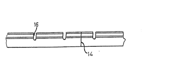
In a wafer provided with means 16 for cutting off
linkage between crystals in a heteroepitaxial crystal layer,
which is a more preferred embodiment of the present invention,
it is possible to prevent the propagation of crystal defects
by those cut-off means. Figure 11 is a plan view showing a
wafer which is provided on the inside of its outer peripheral
portion with a trench 16 for cutting off the linkage between
crystals. Figure 17 is a sectional view showing a section of
such a wafer. When the wafer shown in Figure 11 is worked to
form a semiconductor device, crystal defacts 15 propagated
along the plane of the crystal layer are stopped by the trench
16, which prevents crystal defects 15 from propagating toward
:. - :
~ ~, . . .
.1 ;. ' ~ " ' . ' ~ ' ' " ' ' ' ` ` , ' ' ' , ' ' ': ~ ' ' . . ' ' ' .
- 2028808
::~
- 13
the inner zone. Figure 12 is a plan view showing the effect
of the trench 16.
~As shown in Figure 17, the trench 16 preferably has
- a depth exceeding the thickness of the epitaxial crystal
`~5 layer. As shown in Figure 18, propagation of the crystal
~de~ects 15 is prevented by formation of the trenches 16,
-~whereby only a portion close to the crystal defects 1~, 15
defines a defective chip 18 and good chips }7 can be obtained
-in other regions. Thus, it is possible to remarkably improve
`,10 the fabrication yield of semiconductor chips.
Although the trench is formed along the outer
peripheral portion of the wafer in the aforementioned example,
such a trench may be formed in dimensions corresponding to one
element of the chip. Figure 13 shows examples of such
,15 trenches 26 forming a grid pattern.
¦Another means for cutting off linkage between
crystals is the removal of a portion including defects, in
addition to formation of a trench, which is formed as a groove
~by etching. Figure 14 shows a wafer from which an outer
:$20 peripheral portion 36 of an epitaxial crystal layer including -
~isuch defects has been removed.
Still another cut-off means includes the covering
of an outer peripheral portion of the substrate including a
large number of crystal defects with a film of SiXNy, sixoy or
i25 the like, in order to cause a selective growth only in a
dislocation free portion.
Example 1
A dislocation free GaAs substrate obtained by the
~,VCZ method and a generally used substrate still having crystal
130 defects left in its outer peripheral portion were compared and
studied as follows:
Heteroepitaxialwaferswereprepared by successively
growing P-type AlxGal xAs (x = O. 3) layers of 100 ~m as first -~
layers, P-type AlxGa1xAs (x = 0.02) light emitting layers as
second layers, and N-type AlXGal xAs (X = 0.4~ layers as third
'' ` :'
: , ' .
.
2028808 ::
layers on circular GaAs substrates of 350 ~m in thickness and
75 mm in diameter.
After completion of the epitaxial growth, crystal
defect distributions in the epitaxial layers and in the
~ 5 substrate were observed through X-ray topographic observation,
`~ whereby it was recognized that crystal defects were
transferred toward the N-type A1xGalxAs layer, the third
layer, in the conventional substrate.
On the other hand, no transfer or propagation of
crystal defects was recognized in the dislocation free
~ substrate.
i A heteroepitaxial wafer having such a crystal
structure is mainly applied in an infrared LED etc. The above
~ heteroepitaxial wafers were employed and subjected to working
¦ 15 for forming a device, to evaluate in-plane distributions of
the emission strength. In the conventional wafer, portions
having a low emission strength were unevenly distributed in
a portion still having crystal defects left. Further, the
portions having low emission strength spread toward the wafer
center portion, which had no crystal defects, after epitaxial
I growth. In the dislocation free epitaxial wafer, on the other
I hand, the emission strength of at least 2 mW was attained
uniformly over the entire surface.
Then, in accordance with another aspect of the
present invention, the outer peripheral portion, still having
crystal defects left therein, was removed from the
conventional epitaxial wafer by etching. Thereafter, working
was performed to form a semiconductor device. The in-plane
distribution of the emission strength was evaluated in the
epitaxial wafer to which this technique was applied, whereby
it was possible to attain an emission strength of at least 2
mW over the entire surface. A sample which was first worked
to form a semiconductor device thereby leaving crystal defects
I in its outer peripheral portion. Then the portion with
. .
35 defects was removed by etching. The resulting product was ~ -
observed through X-ray topography prior to and after the
202880~
.
etching, whereby it was found that slips propagated toward the
wafer center portion in the product prior to etching while no
crystal defects were observed in any portion of the product
after the etching.
Similar phenomena were investigated on
heteroepitaxial layers of InGaP and InGaAsP provided on GaAs
substrates. Such crystal layers are employed in short
wavelength lasers. Similar phenomena were also observed in
these crystal layers, and it was recognized that the same had
problems common to heteroepitaxial wafers having substrates
of GaAs and the present invention is also effective on
compound semiconductors.
Example 2
A dislocation free InP substrate obtained by the VCZ
method and a generally used substrate still having crystal
defects left in its outer peripheral portion were compared and
studied as follows: Circular substrates of 350 ~m in
thickness and 50 mm in diameter were divided into halves.
These halves of the substrates were abutted against each other
to cause simultaneously epitaxial qrowth on both halves. The
epitaxial layers were successively grown in structures of InP
layers of 2 ~m in thickness for first layers, InGaAs layers
of 5 ~m in thickness for second layers, and InP layers of
2 ~m in thickness for third layers.
After the epitaxial growth, a distribution of
crystal defects was observed by an etching method, to
recognize that crystal defects were transferred toward the InP
layer, the third layer, through the InGaAs layer in the outer
peripheral portion of the conventional InP substrate. In the
dislocation free InP substrate fabricated by the VCZ method,
. . ..
on the other hand, no crystal defects were observed in the
respective epitaxial layers. In addition, no crystal defects -
were observed in an X ray topographic observation. Thus, it
was confirmed that the transfer of crystal defects recognized " `-
35 in the conventional InP substrate was not caused by epitaxial ;~
. ', `:':: ' ::
: - ~-
2028808
16
growth, but the cause therefor was the defective InP single
; crystal substrate as used.
~; Crystals having such crystal structures are mainly
~; applied to a long waveband light emitting element, a PIN
photodiode, and the like. The aforementioned respective
epitaxial wafers were employed and processed to measure dark
!, currents, which are noise components, to find that portions
having high dark currents were unevenly distributed in an area
~J still having crystal defects in the conventional wafer.
Further, it was recognized that portions having high dark
!l currents were also propagated to the wafer center area, which
initially had no crystal defects, after the epitaxial growth.
On the other hand, the dislocation free epitaxial
after exhibited an excellent dark current characteristic of
not more than 3 x 10⁻⁷ A/cm2 when a voltage of -5 V was applied
¦ to the entire surface without depending on locations. To this
end, it is possible that slips in the outer peripheral portion
of the wafer linearly extend toward the central area in heat
treatment applied to the device. It was recognized that the
portions having high dark currents, i.e., portions in which
the dark current values were at least 3 x 10 7 A/cm2 at a
voltage of -5 V, existed as an extension of the outer
peripheral portion of the wafer of two inches, toward the
central area, in correspondence to the distribution of the
crystal defects as observed by etching.
In general, it was impossible to use a wafer of a
circular configuration just obtained by slicing an ingot due
to the restriction imposed on the epitaxial growth technique,
and a rectangularly cut substrate has been employed
conventionally. However, it was recognized that, even if a
wafer of a circular configuration just obtained by slicing an
ingot was used, portions which had been removed by cutting
could not be used since crystal defects of the substrate were
directly transferred to epitaxial crystal layers. It was
further recognized that slips in the outer peripheral portion
of the wafer were propagated toward a part of the substrate
~ :~' "` '',`,
2~)2~8~
17
center portion or area having a low crystal defect density and
portions attaining excellent dark current characteristics were
reduced as compared with the case of employing a rectangularly
cut substrate.
Then, a heteroepitaxial layer was removed in the
form of a groove or trench prior to a heat treatment of the
device, the groove extending along an outer peripheral portion
of the epitaxial wafer still having crystal defects in its
peripheral portion. Thereafter, 5000 devices were similarly
formed. In-plane distributions of dark currents were measured
on the area enclosed by the trench to check whether there were
more than 100 devices of at least 3 x 10 7 A/cm2 among the
total of 5000. An X-ray topographic observation was
simultaneously performed and no crystal defects such as slips
were discovered. Thus, it is possible to obtain a larger
number of semiconductor devices from one wafer as compared
with the prior art, thereby remarkably improving the yield,
by forming a trench in accordance with the present invention
while causing an epitaxial growth on a dislocation free
substrate.
Example 3
A dislocation free substrate obtained by the VCZ
method and a conventionally used substrate still having
crystal defects in its outer peripheral portion were used for
wafers provided with heteroepitaxial layers of InGaAsP, and
these wafers were studied and compared. Circular substrates
were produced with a first layer 350 ~m thick, a second layer
l ~m thick, and a third layer of InP 2 ~m thick. The second
layers were InGaAsP structures of 1.3 ~m in emission strength.
After completion of the epitaxial growth, crystal defect
distributio~s in the epitaxial layers and in the substrates
were observed through X-ray topography, whereby it was found
that the conventional substrate included crystal defects
toward the third InP layer.
On the other hand, no transfer of crystal defects
was observed in the dislocation free substrata. An apitaxial
:, ~ .: . .: . -
.~. 18 2028~08 :
.. :
wafer having such a crystal structure is mainly applied to along wavelength LED etc. The aforementionled heteroepitaxial
wafers were employed and subjected to processing for making
semiconductor devices to evaluate peak inverse voltages,
emission strength, emission form defects and respective in~
plane distributions.
s In the conventional wafer, the peak inverse voltage
was lowered (< 1 V) in a portion still having crystal defects,
and the emission strength was also lowered. The emission orm
was also defective. It was observed through X-ray topography
that these crystal defects propagated after processing toward
a portion having had no crystal defects after heteroepitaxial
growth.
In the InGaAsP heteroepitaxial layer provided on the
dislocation free substrate, on the other hand, no crystal
! defects were observed after epitaxial growth and after
processing. The peak inverse voltage was > 2 V, while the
emission strength was uniform in the plane and no defect of
the emission form was observed.
While nondefective devices were not more than 1000
in the conventional wafer, it was possible to obtain at least
4000 nondefective devices in the dislocation free
heteroepitaxial wafer, whereby the yield was remarkably
improved.
The compound semiconductor wafer according to the
present invention is applicable to a semiconductor device such
as a photoreceptor e.g. a PIN photodiode, a laser and a light
emitting element; an LED, and an amplification element; or an
FET.
:': :'
`: . '' :
., :' ' '
, .. ' ' ` ' .'::