Note: Descriptions are shown in the official language in which they were submitted.
2028851
SPECIFICATION
PREPARATION AND REPRODUCTION OF FILTERS AND PREPARATION OF
FILTER PHOTOGRAPHIC MATERIALS
TECHNICAL FIELD
The present invention relates to preparing and
reproducing filters and preparing filter photographic
materials. More particularly, this invention is concerned
with preparing and reproducing color filters by the
application of holography and preparing filter photographic
materials well-suited for recording electrostatic images.
BACKGROUND TECHNIQUE
Color filters so far used in various fields are of the
dyed type. Because of their processes of preparation being
complicated, however, it has been attempted to prepare color
filters by the application of holography.
Figure 1 is a view for illustrating a conventional
process for making color filters by the application of
holography.
Referring to Fig. 1, a photosensitive or photographic
material 12 is located in opposition to a mirror 13 and a
mask il having a striped pattern, for instance, is brought
into close contact with the material 12. Light incident from
- i -
~0~88~1
above the mask 11 is reflected from the mirror 13 to make an
interference fringe, which is in turn recorded in the
photographic material 12 to prepare a color filter.
When dirt, dust, etc. are present between the
photographic material and the mask in close contact with it,
the gap varies, giving rise to the shading-off of the mask
image. Thus, a serious problem with such a conventional
process as shown in Fig. 1 is that a considerable difficulty
is encountered in bringing the photographic plate in
constantly close contact with the mask in a certain
relation.
Even though the close contact is achieved at a certain
interval, it is most likely that the mask image may shade
off due to the thickness of the photographic material
itself.
Color filters heretofore used are of the dyed type.
Figure 2 is a view showing a conventional process for
making the dyed type of color filters.
As illustrated, a gelatine layer is first coated on a
glass substrate 21 and then subjected to pattern exposure to
form a gelatine pattern layer. Next, a dye is fixed to the
gelatine pattern layer 23 by treatments with, e.g., tannic
acid to make a monochromatic pattern filter. A color filter,
which may be in striped, mosaic or other forms, is obtained
by repeating the pattern exposure and the formation of the
gelatine and dyed pattern layers for each of three colors.
A problem with such a conventional process for making
- 2 -
~a~885~
the dyed type of color filters as shown in Fig. 2, however,
is that its process of preparation is too complicated to
increase the production cost. Another problem is that it is
difficult to make a pattern of sufficient resolution.
Still another problem is that a serious difficulty is
experienced in getting the overlapping chromatic images in
correct registration, since it is required to carry out
pattern exposure for each of three colors cyan, magenta and
yellow or red, green and blue.
On the other hand, silver salt photography is known as a
high-sensitivity photographic technique, in which a
photographic image is recorded on a film or the like through
a developing step. The image is reproduced with a silver
salt emulsion (photographic paper, etc.) or displayed on a
cathode ray tube (CRT for short) by the optical scanning of
the developed film.
There is also now available an electrophotographic
technique. According to this technique, an electrode is
deposited onfio a photoconductive layer, the photoconductor
is electrified on its overall surface by corona
electrification in a dark place and then exposed to intense
light to make a light-striking region electrically
conductive. That region is then rid of charges to optically
form an electrostatic latent image on the surface of the
photoconductor. Finally, a toner having charges of polarity
different from or identical with that of the residual
charges is deposited onto the latent image for development.
- 3 -
~o~s~~~
This is primarily used for copying purposes, and cannot be
used for photographic purposes due to its low sensitivity.
Also, toner development should usually be carried out just
after the formation of the latent image, because the
retention time or duration electrostatic charges is short.
According to a further technique now available - a TV
photographic technique, the original image is picked up by a
pickup tube, and the image-carrying information obtained by
making use of an optical semiconductor is outputted in the
form of electrical signals, which are immediately used to
make an image on a CRT. Alternatively, the signals may be
recorded on a video tape or the like by magnetic recording
hardware for making an image on the CRT at any desired time.
The silver salt photographic technique provides an
excellent means for preserving the original image, but needs
not only a developing step for making a silver salt image
but also sophisticated optical, electrical or chemical
processings from hard copying to soft copying (CRT
displaying) for the reproduction of the image.
Electrophotography provides a simpler and faster
development of the obtained later image than does the silver
salt photographic technique, but is much inferior in the
dissociation of a developer, image quality, etc. to the
silver salt technique, because the duration of the latent
image is very short.
TV photography needs line sequential scanning for
outputting or recording the electrical image signals
_ q, _
2028851
obtained by the pickup tube. The line sequential scanning is
performed either by electron beams in the pickup tube or by
a magnetic head for video recording. However, this recording
technique is much inferior to planar analog recording such
as silver salt recording, because its resolution is
dependent upon the number of the lines to be scanned.
This is again true of the resolution of a TV
photographic system now under development, which makes use
of a solid photographic element (CCD, etc.)
The problems associated with these techniques imply that
the higher the quality and resolution of the recorded image,
the more complicated the processing steps, or the simpler
the processing steps, the poorer the storing or memory
function, the image quality, etc.
The inventor has applied a patent application (Japanese
Patent Application No. 63(1988)-121592 for a process for
recording and reproducing electrostatic images, wherein a
photographic material comprising a photoconductor layer
having an electrode formed on its front surface and a charge
carrier medium comprising a charge carrier layer having an
electrode formed on its rear surface are located on an
optical axis in opposite relation, and the assembly is then
exposed to light while applying voltage between both the
electrodes to form on the charge carrier medium an
electrostatic latent image corresponding to the incident
optical image.
According to this process for recording and reproducing
- 5 -
X028851
electrostatic images, the photographic material is provided
by laminating a photoconductive layer on an electrode, and
is located in opposition to the charge carrier medium,
following by pattern exposure for the photographic plate
while voltage is applied between both the electrodes,
thereby accumulating imagewise charges in the charge carrier
medium. In this instance, a color filter may be located in
the optical path in front of the photographic material to
make a color image. The color filter may be spaced away
from, or made intergral with, the photographic material.
However, much labor and time are required to laminate
the color filter individually on the photographic plate.
The present invention seeks to provide a process for
preparing a precise color filter by recording a sharp mask
image in a photosensitive or photographic material with no
need of bringing a mask into precisely close contact with
the photographic material.
Another object of this invention is to provide a process
for reproducing a color filter which uses a hologram capable
of achieving sufficient resolution while dispensing with a
photolithographic step, precise alignment or registration,
etc.
A further object of this invention is to provide a
process for providing an efficient lamination of a filter on
a photographic material used in recording electrostatic
images.
- 6 -
~U2~8a1
DTSGLOSURE OF THE INVENTION
:Briefly, the present invention is characterized in that
a photographic material and a mask having a given pattern
are located at a given interval in opposite relation and are
illuminated with light from the opposite directions to make
a hologram, and then the hologram is located in opposition
to the photographic material at a given distance therefrom
and is illuminated with light through the photographic
material, thereby recording in the photographic material an
interference fringe made by the light reflected arid
diffracted by the hologram and the illumination light.
With this arrangement wherein the mask image can be
reproduced in the photographic material with no need of
bringing the mask into precisely close contact with the
photographic material, it is possible to prepare a precise
holographic color filter without causing the shading-off of
the mask image.
The present invention is also characterized in that a
master hologram having R, G and B patterns recorded therein
is located in opposition to a photographic material, and is
then illuminated with light in which three colors R, G and B
are mixed together, thereby transferring and reproducing on
the photographic material an interference fringe made by the
light reflected and diffracted from the hologram and the
illumination light. ,
With this arrangement wherein the image reproduced from
_ q _
a
2U28851
the master hologram can be reproduced in the photographic
material at one exposure operation, it is possible to
dispense with a photolithographic step, precise alignment or
registration, etc.
Further, the present invention provides a process for
forming a filter photographic material by providing a filter
layer on a photographic material obtained by laminating a
transparent electrode layer and a photoconductive layer
successively on a transparent support, characterized in that
a first laminate in which the filter layer and an adhesive
layer are laminated successively on 'the support and a second
laminate in which the photoconductive and transparent
electrode layers are laminated successively on a carrier
film through a release layer are laminated together, while
the adhesive layer of the first laminate is located in
opposition to the transparent electrode layer of the second
laminate, followed by removal of the carrier film.
Still further, the present invention provides a process
for making a filter photographic material by providing a
filter layer successively on a photographic material
obtained by laminating a transparent electrode layer and a
photoconductive layer successively on a transparent support,
characterized in that a laminate in which the falter layer
and an adhesive layer are laminated successively on a
carrier film through a release layer and the photographic
material in which the transparent electrode and
photoconductive layers are laminated successively on the
- 8 -
CA 02028851 1999-07-28
i
transparent support are laminated together, while the
adhesive layer of the laminate is located in opposition to
the support of the photographic material, followed by
removal of the carrier film, or simultaneously with only the
filter layer alone being formed on the back side of said
photographic material by heat transfer using a thermal head.
BRIEF DESCRIPTION OF THE DRAWINGS
Figure 1 is a view for illustrating a conventional
(prior art) process for making a color filter with the aid
of holography,
Figure 2 is a view showing a conventional (prior art)
process for making a dyed type of color filter,
Figures 3 and 4 each are a view for showing the process
for making a color filter according to this invention,
Figure 5 is a view for illustrating the process for
reproducing a color hologram according to this invention,
Figure 6 is a sectional view of a laminate used with the
process for making a filter photographic material according
to this invention,
Figure T is a sectional view of the filter photographic
material made by this invention,
Figure 8 is a sectional view of a laminate used with
another process for making a filter photographic material
according to this invention,
_ g _
202~~51
Figure 9 is a sectional view of a filter photographic
material made by a further process of this invention.
Figure 10 is a schematic view of a heat transfer unit
used with a still further process of this invention,
Figure 11 is a view for illustrating how to record
electrostatic images,
Figure 12 is a view illustrating how to read potentials
in a d.c. amplification manner, and
Figure 13 is a view of a general structure of how to
reproduce an electrostatic image.
BEST MODE FOR CARRYING OUT THE INVENTION
One embodiment of the process for making a color filter
according to this invention is illustrated in Figs. 3 and 4,
wherein reference numeral 31 stands for a photographic
material, 32 a mask, 33 and 34 illumination beams, 35 a
photographic material, and 36 reconstructed and reference
beams.
As illustrated in Fig. 3, the photographic material 31
is spaced away from the mask 32 at a given interval D. The
mask 32, for instance, has a striped pattern. The
photographic material 31 and the mask 32 are illuminated
with the beams 33 and 34 frora the opposite directions. The
light 32 transmitted through the mask 32 - referred to as
the object light - and the reference light 33 make an
interference fringe which is in turn recorded in the
- 10 -
~028~51
photographic material 31 to prepare a Lippmann hologram.
As illustrated in Fig. 4, the thus prepared hologram 31
is located at a given distance from the photographic
material 35, and is then illuminated with the light 36
through the photographic material 35. In consequence, the
Iight diffracted from the hologram and the illumination
light 36 forms an interference fringe (the mask image) at a
location spaced away from the hologram 31 by the distance D,
where the photographic material 35 is positioned such that
it overlaps with the mask image. Since the photographic
material can be superposed on the mask image in this manner,
the mask image can be recorded much more sharply without
causing it to shade off, rendering it possible to make a
precise color filter. Thus, any precisely close contact of
the photographic material with the mask can be dispensed
with.
It is understood that if exposure is repeated three
times at different mask positions using red, green and blue
beams as the illumination beams 33 and 34, it is then
possible to record a striped image of red, green and blue in
a single photographic material. It is thus possible to
prepare a color filter by reconstructing and recording the
striped image of red, green and blue using red, green and
blue beams as the light 36.
It is again possible to prepare a color filter by
recording striped images of red, green and blue in three
photographic materials and making records at different mask
- 11 -
. .
2028851
positions at the time of reproduction.
According to the process described with reference to
Figs. 3 and 4, it is thus possible to make a very sharp mask
image by superposing the photographic material on the
position of the mask image reconstructed with neither need
of bringing the photographic material into precisely close
contact with the mask nor fear of shading off the mask
image.
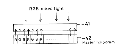
How to reproduce a color hologram usable as a filter is
illustrated in Fig. 5, wherein reference numeral 41 stands
for a photographic material and 42 a master hologram.
Referring to Fig. 5, the master hologram 42 is a
Lippmann hologram having regions in which interference
fringes of red, green and blue are recorded individually.
The photographic material 41 is located in opposition to the
master hologram 42. As the hologram 42 is illuminated from
above the material 41 with light obtained by mixing of red,
green and blue, the light diffracted from the hologram 42
and the incident light make an interference fringe, which is
in turn recorded in the photographic material 41. In this
manner, the pattern of the master hologram 41 is transferred
and reproduced on the photographic material 42 at one
exposure operation.
It is noted that there is too large a gap between the
photographic material and the master hologram, some light
reflected from the adjacent region enters through it, making
an interference fringe, which: is then recorded in the same
- 12 -
~o~~~~~
place, shading off the mask image. Hence, the gap between
both should be reduced as much as possible. For instance,
such a gap should preferably be determined depending upon
how large the pattern is, for instance, be one half or less
of an inter-stripe gap in the case of a striped type of
filter.
It is understood that while the foregoing embodiment has
been described specifically with reference to a striped
filter, the present invention may equally be applicable to
other filters such as a meshed filter.
According to the process described with reference to
Fig. 5, it is possible to reproduce the master hologram at
one exposure operation and so make a color hologram of
excellent resolution without needing precise alignment or
registration.
A specific embodiment, in which a color filter is
applied to recording electrostatic latent images, will now
be explained with reference to processes for making a
photographic material having a color filter.
Figs. 6a and 6b are schematic sections of first and
second laminates, respectively, used with the processes for
making a photographic material with a color filter, and Fig.
Z a sectional view of a photographic material with a color
filter made by a first process. In these drawings, reference
numeral 41 stands for a general structure of a photographic
material with a color filter, 44 a color filter, 45 a
support for the photographic material, 46 an adhesive layer,
- 13 -
CA 02028851 1999-07-28
4T a photographic electrode, 48 a release layer, 49 a
photoconductive layer and 50 a carrier film.
The filter photographic material produced by the first
process of this invention is of a structure wherein the
support 45, filter 44, adhesive layer 46, photographic
electrode 4T and photoconductor 49 are successively
laminated together, as shown in Fig. Z.
This filter photographic material is prepared by
laminating together a first laminate shown in Fig. 6a with a
second laminate shown in Fig. 6b, while the adhesive layer
46 of the first laminate is located in opposition to the
photographic electrode 4T of the second laminate.
The first laminate is formed by laminating the filter 44
and adhesive layer 46 successively on the support 45.
The filter may be a layer formed by coating a
photographic material such as a silver salt, gelatine
bichromate or a photopolymer, e.g., a photoresist on the
support 45. At this stage, the layer may be colored or dyed
in red, green and blue or allowed to bear a hologram, dots,
an image, characters or marks. This layer has a function of
providing the photoconductive layer with a pattern.
For instance, the color filter may be formed by any one
of the following known methods. According to one method, a
photoresist is first coated on a support to form a film.
Then, the film is exposed to light through a mask pattern to
form a striped pattern, which is in turn dyed in red, green
and blue. According to another method, prismatic light is
- 14 -
202885.
passed through narrow slits to form an interference fringe
of red, green and blue, which is in turn recorded on a
holographic recording medium. According to still another
method, a photoconductor with a mask in close contact with
it is exposed to light to form a striped pattern of red,
green and blue by an electrostatic latent image. The striped
pattern is then toner-developed and transferred three times
for color mixing, thereby forming a toner stripe. The thus
obtained filter defines one pixel as fine as 10 ~Zm by a set
of red, green and blue.
In addition to such color filters, use may also be made
of holographic, dyed, pigmented or interference filters.
The film layer formed on the support is provided thereon
with an adhesive layer for bonding to the second laminate.
The adhesives, which should be transparent, may be coated on
the film by suitable means such as spinner or blade coating,
if required, after dissolved in a solvent.
The second laminate shown in Fig. 6b will now be
explained.
The second laminate is formed by laminating the
photoconductive layer 49 and transparent electrode layer 4Z
successively on the carrier film 50 through the release
layer 48.
The carrier film may have a strength sufficient to
support the photoconductor 49 and transparent electrode
layer 4f and so may be formed of paper, a plastic film or
sheet or the like. The release layer provided on the carrier
- 15 -
2028851
film may be formed of a material based on silicone, fluorine
or other resin, which is dissolved in a polar solvent for
coating. ,
The photoconductive layer laminated an the release layer
is a semiconductor layer which generates light carriers
(positive holes and electrons) upon irradiated with light
and has a function of transporting them. To this end, an
inorganic photoconductive material such as amorphous
seleniura, amorphous silicon, zinc oxide, cadmium oxide or
lead oxide may be coated on the release layer with a binder,
a solvent and so on by suitable means such as vapor
deposition, sputtering, plasma CVD, ECRCVD or MOCVD.
Alternatively, an organic photoconductive material may be
coated on the release layer with a binder, a solvent and so
on. As the organic photoconductive material, use may be made
of either one of a single layer system having both charge-
generating and-transporting functions and a so-called
function-separation type of laminate system in which the
charge-generating function is separate from the charge-
transporting function. Typical of the former are single-
layer photosensitive systems comprising mixtures of PVK-TNF,
PVK-triphenylmethane type dye, PVK-pyrylium type dye and PVK-
xanthene type dye, and typical of the latter mixed systems
in which the charge generating layers comprise dispersion
systems of, e.g., azo type pigment-binder and phthalocyanine-
binder while the charge transporting layers comprise
mixtures of binders with materials based on hydrazone,
- 16 -
20288x1
pyrazoline, polyvinylcarbazole (PVK), carbazole, oxazole,
triazole, aromatic amine, amine, triphenylmethane and
polycyclic aromatic compounds. The inorganic photoconductive
materials may be used in combination with the organic
photoconductive materials and organic charge transporting
materials.
The support 45 may have a certain strength sufficient to
support the photographic material. Although the support 45
is not critical in terms of thickness and material, it
should be transparent. To this end, use may be made of a
rigid material such as glass or plastic sheets, but
preference is given to a transparent glass sheet or a
transparent film or sheet of flexible plastics, all having a
thickness of about 1 mm.
The electrode 4T, which is provided on the support 45,
may be formed of any material having a specific resistance
of 106~~cm or less. To this end, use may be made of a
conductive film of a semitransparent inorganic metal or
transparent metal oxide or an organic conductive film of a
quaternary ammonium salt, etc. Such an electrode 4T is
formed on the support 45 by suitable means such as vapor
deposition, sputtering, CVD, coating, plating, dipping and
electropolymerization. However, the electrode 4T should vary
in thickness depending upon the electrical properties of the
material forming it and the voltage applied for the
recording of information. Like the support 45, the electrode
4? has to possess such optical properties as mentioned
- 1~ -
2~2~851
above. For instance, if the information-bearing light is
visible light (400-?00 nm), use may then be made of a
transparent electrode obtained by the sputtering or vapor
deposition of a material such as ITO (In203-Sn02) or Sn02 or
the coating of an ink composition comprising finely divided
powders thereof and a binder; a semitransparent electrode
prepared by the vapor deposition or sputtering of a metal
such as Au, A1, Ag, Ni or Cr; and an organic transparent
electrode obtained by the coating of an organic material
such as tetracyanoquinodimethane (TCNQ) or polyacetylene.
The above-mentioned electrode materials may also be used
in the case where the information-bearing light is infrared
light ('100 nm or more). In some cases, a colored electrode
capable of absorbing visible light may be used so as to cut
off visible light.
Basically, the above-mentioned electrode materials may
be used even in the case where the information-bearing light
is ultraviolet light (400 nm or below). However, the use of
a support material absorbing ultraviolet light (such as an
organic polymeric material and soda glass) should be
avoided. Preferable to this end is a material such as quartz
glass, which can transmit ultraviolet light therethrough.
Additionally, an anti-reflection layer be provided on the
surface on which light is incident, i.e., on the support 45
in Fig. Z or on the filter 44 in Fig. 9. The anti-reflection
layer may be formed of a single or plural thin films
obtained by the sputtering, vapor deposition or other
- 18 -
X028851
processing of an inorganic material such as magnesium
fluoride or titanium oxide.
According to this invention, the thus formed second
laminate and the aforesaid first laminate are laminated
together. As illustrated in Figs. 6a and 6b, the laminates
provided in sheet forms may be bonded together and then cut
to a size well-fit for photographic material. Alternatively,
the support 45 of the first laminate and the carrier film 50
of the second laminate may be formed of plastic films so as
to provide both the first and second laminates in roll
forms. By doing so, it is possible to carry out continuously
the steps of bonding together the first and second
laminates, releasing the carrier film and cutting the
resulting laminate to a size well-fit for photographic
material.
The laminate used with the second process according to
this invention and the photographic material prepared
thereby will now be explained with reference to Figs. 8 and
9, respectively.
As illustrated in Fig. 9, the photographic material is
formed by laminating the filter layer 44 on one side of the
support 45 through the adhesive layer 46 and laminating the
transparent electrode layer 4Z and photoconductive layer 49
successively on the other side of the support 45. This
photographic material is prepared by bonding the laminate,
in which the filter 44 and adhesive layer 46 are laminated
through the release layer 48 on the carrier film 50 shown in
- 19 -
2o28~a~1
Fig. 8a, at that adhesive layer 46 to the support 45 of the
photographic material shown in Fig. 8b, followed by removal
of the carrier film 50 and release layer 48.
The materials forming the respective layers of the
photographic material shown in Fig. 9 may be the same as
those mentioned in connection with the process for making
the above-mentioned first photographic material, and may be
larainated together in the same manner as mentioned in
connection with the above-mentioned first process.
In accordance with this second process, the laminate
provided in sheet form may be cut to a size well-fit for
photographic material, followed by removal of the carrier
film. Alternatively, the photographic material may be
provided in usable form as shown in Fig. 8b, and only the
filter layer 44 may then be transferred onto the
photographic material 41 through the adhesive layer 46 with
the aid of a thermal head, as shown in Fig. 10, while making
use of the releasability of the filter layer 44. In this
case, if a continuous length type of laminate is used as the
laminate shown in Fig. 8a, it is then possible to automate
the preparation of filter photographic materials by
transferring filter layers continuously on photographic
materials, while moving it.
Referring now to Fig. 11, how to record electrostatic
images will be explained. Tn this figure, reference numeral
41 stands for a filter photographic plate, 43 a chaxge
carrier medium, 51 a charge carrier layer, 53 an electrode
- 20 -
CA 02028851 1999-07-28
for the charge carrier medium, 55 a support for the charge
carrier medium, and 5T a power source.
The charge carrier medium 43, on which an electrostatic
latent image is to be formed through the photographic
material, is formed by laminating the charge carrier layer
on the electrode 53, and comprises a high molecular material
of insulating properties so high as to prevent the migration
of charges. In other words, this material is required to
have such insulating properties as expressed in terms of a
specific resistance of 1014~~cm or above. Also, the high
molecular material forming the charge carrier layer is
required to have a glass transition temperature higher than
an ambient temperature at which it is to be used.
Such a high molecular material may be any one of
thermoplastic resin, heat curing resin, ultraviolet curing
resin, radiation curing resin such as electron beam curing
resin and engineering plastics. The thermoplastic resins,
for instance, may include fluorine resins such as
polytetrafluoroethylene, fluorinated ethylene propylene,
tetrafluoroethylene-perfluoroalkylvinyl ether copolymers or
their dispersion or modified (coating) versions; polyether
ether ketone resin; polyp-xylene); and so on. These resins
may be coated, vapor-deposited or otherwise provided on the
electrode 53 in layer form.
Fig. 11 provides an illustration of how the
electrostatic latent image is formed on the charge carrier
medium 43 by exposing it to light from above the
_ 21 _
202881
photographic plate 41.
As illustrated, the charge carrier medium 43 is
positioned with respect to the photographic plate 41 through
a gap of about 10 kZm. This charge carrier medium 43 is
provided by vapor-depositing a 100 A-thick aluminium
electrode on the support 55 comprising a lmm-thick glass and
then forming the charge carrier layer 51 on this electrode.
As illustrated in Fig, lla, the charge carrier medium 43
is arranged with respect to the photographic plate 41
through a gap of about 10 kZm. Then, voltage is applied from
the power source 5? between the electrodes 4? and 53, as
illustrated in Fig. 11b. Since the photoconductive layer 49
is a high resistor in a dark plane, no change takes place
between the electrodes. If a voltage higher than the firing
voltage according to the Paschen's law is applied across the
gap depending upon the magnitude of the impressed voltage or
a leakage current from the substrate electrode, then
discharge occurs across the gap, forming electrostatic
changes corresponding to a dark current on the charge
carrier medium. As light is incident from the photographic
plate 41 through the filter 44, light carriers (electron
holes) are generated on a portion of the photoconductive
layer 49 on which the light strikes. Then, charges of the
polarity opposite to that of the charge carrier medium's
electrode migrate from within toward the surface thereof,
during which upon the voltage across the air gap exceeding
the firing voltage according to the Paschen's law, corona
- 22 -
2428~~~.
discharge takes place with respect to the charge carrier
layer 51 or charges are pulled out of the photoconductive
layer 49 due to field emission, so that charges are
accelerated by the field and thus accumulated on the charge
carrier layer 51.
After the exposure has been complete, the voltage is put
off as illustrated in Fig. llc, and the charge carrier
medium 43 is then removed as shown in Fig. 11d, making the
formation of an electrostatic latent image complete.
At the time when the image is accumulated in the form of
information-bearing charges, an insulating protective film
may be laminated on the charge carrier layer. It is noted
that recording is possible from above the protective film,
if it has a thickness of 0.4 ~Zm or below. Thus, the
information-bearing charges can be stored over an extended
period of time, whether in a dark or bright place. Also,
whether stored on the surface of the charge carrier layer or
microscopically trapped in electron or hole forms in the
vicinity of the surface of the insulator, the information-
bearing charges are stored over an extended period of time.
Inputting information to the charge carrier medium may
be achieved by using a high-resolution electrostatic camera
or Laser. Referring first to the high-resolution
electrostatic camera, a recording medium is constructed
using a photographic material and a charge carrier medium in
place of a usual photographic film. Voltage is applied
between both electrodes to make the photoconductive layer
- 23 -
CA 02028851 1999-07-28
electrically conductive and so accumulate charges on the
charge carrier layer depending upon the quantity of incident
light, whereby an electrostatic latent image corresponding
to the inputted optical image is formed on the charge
accumulating medium, To this end, a shutter of either the
mechanical or electrical type may be used. The electrostatic
latent image can be stored over an extended period of time,
whether in a dark or bright place.
When the filter 44 is a color filter for separating
optical information prismatically into red, green and blue
components to obtain it in the form of parallel beams, one
frame may be defined by three sets of the charge carrier
media subjected to the R, G and B separation for color
photography. To this end, one frame may also be formed by
one set of R, G and B images arranged on one plane.
For laser recording, argon laser (514 nm, 488 nm),
helium-neon laser (633 nm) or semiconductor laser (T80 nm,
810 nm, etc.) may be used as the light source. Voltage is
then applied with a photographic material being brought in
close planar contact with or in opposition to a charge
carrier medium at a certain interval. In this case, the
photographic electrode may be the same polarity as that of
the carrier of the photographic material. In that state,
laser exposure corresponding to imagewise, literal, cord or
line signals is carried out by scanning. Analog recording
for information such as picture images is carried out by the
modulation of the light intensity of laser beams, while
- 24 -
CA 02028851 1999-07-28
digital recording for characters, cords or line pictures is
effected by the on-off control of laser beams. Dotted
imaging may also be carried out under the dot generator on-
off control of laser beams.
Reference will now be explained with reference to how to
reproduce the recorded electrostatic image.
An example of how to read potentials in the process for
reproducing an electrostatic image on the charge carrier
medium according to this invention is illustrated in Fig. 12
wherein like reference numerals of Fig. 6 refer like parts.
It is noted that reference numeral 61 stands for a potential
reader section, 63 a detection electrode, 65 a guard
electrode, 67 a capacitor and 69 a voltmeter.
When the potential reader section 61 is located in
opposition to the surface of the charge carrier medium 43 on
which charges are built up, the detection~electrode 63 is
subjected to an electric field defined by the charges
accumulated on a charge carrier 51 of the charge carrier
medium 43, thus generating on its surface induction charges
in the amount equal to that of the charges of polarity
opposite to that of such induction charges in the same
amount, there is a potential difference corresponding to the
accumulated charges across the capacitor's electrode, which
is in turn read on the voltmeter 69, thereby determining the
potential of the charge carrier medium. Then, an
electrostatic latent image can be produced in the form of
electrical signals by scanning the surface of the charge
- 25 -
202851
carrier medium with the potential reader section 61. It is
noted that only with the detection electrode 63, there is a
drop of resolving-power under the action of an electric
field (an electric line of force) defined over a range wider
than the region of the recording medium opposite to the
detection electrode; hence, the guard electrode 65 may be
grounded around the detection electrode. According to such a
system, since the electric line of force acts vertically to
the plane, it can be obtained from only the region opposite
to the detection electrode 63. Thus, it is possible to read
the potential of a region having an area nearly equal to
that of the detection electrode. Since the accuracy and
resolving-power of potential reading vary largely depending
upon the geometry and size of the detection and guard
electrodes as well as the space between them and the charge
carrier medium, it is essentially required to design them
while taking into account the optimum conditions to meet the
peformance demanded.
The image-carrying charges on the charge carrier medium
may be reproduced in the form of information through an
electro-optical crystal by exposing the medium to laser
beams, etc. from the electrode of the charge carrier raedium
provided with the anti-reflection layer. In this case, the
charge carrier medium should be formed of a transparent
material, while the electro-optical crystal, which may be '
formed of an electro-optical material such as barium
titanate or lithium tantalate (LiTa03j, may be positioned
- 26 -
~o~ssm
within the optical path.
Fig. 13 is a schematic view showing the process for
reproducing electrostatic iraages according to this
invention, in which reference numeral Z1 stands for a
potential reader, Z3 an amplifier, Z5 a CRT and Z7 a
printer.
Referring to this figure, a charge potential is detected
by the potential reader Z1, and the resultant output is
amplified by the amplifier Z3 for display on the CRT T5 or
printing-out with the printer TT. In this case, the region
to be read may be arbitarily selected and outputted at any
desired time, or may be repeatedly reproduced. With the
electrostatic latent image obtained in the form of
electrical signals, it may then be recorded in other
recording media, if required.
Used with the charge carrier medium, the filter
photographic material is exposed to light from its side
while voltage is applied to it, whereby light carriers
(e.g., holes) generated in the photoconductive layer of the
photographic material are migrated under the action of an
electrical field between it and the charge carrier medium
toward the surface of the photoconductive layer. Then,
discharge occurs across an air gap between the photographic
material and the charge carrier medium or the air layer
there is ionized, thereby recording the exposure pattern
through the filter in the charge carrier medium in the form
of electrostatic charges.
- 2Z -
202~~51
Further, the present invention provides a process for
forming a filter photographic material by providing a filter
layer on a photographic material obtained by laminating a
transparent electrode layer and a photoconductive layer
successively on a transparent support, characterized in that
a first laminate in which the filter layer and an adhesive
layer are laminated successively on the support and a second
laminate in which the photoconductive and transparent
electrode layers are laminated successively on a carrier
film through a release layer are laminated together, while
the adhesive layer of. the first laminate is located in
opposition to the transparent electrode layer of the second
laminate, followed by removal of the carrier film. According
to this process, it is possible to eliminate the
discoloration, fading or other degradation of the filter
layer due to heating applied for the vapor-deposition of ITO
or photoconductive electrodes. In addition, since the filter
can be laminated directly on the ITO electrode through the
adhesive layer, filter photographic materials can be
produced efficiently. Moreover, this process makes the space
required for the support much smaller than that required for
a glass support, and can give a clear electrostatic image to
the charge carrier medium.
Still further, the present invention provides a process
for making a filter photographic material by providing a
filter layer successively on a photographic material
obtained by laminating a transparent electrode layer and a
- as -
2028851
photoconductive layer successively on a transparent support,
characterized in that a laminate in which 'the filter layer
and an adhesive layer are laminated successively on a
carrier film through a release layer and the photographic
material in which the transparent electrode and
photoconductive layers are laminated successively on the
transparent support are laminated together, while the
adhesive layer of the laminate is located in opposition to
the support of the photographic material, followed by
removal of the carrier film. According to this process, the
filter can be easily laminated on the photographic material.
With a laminate of continuous length, filter layers are
transferred onto a number of photographic materials, while
it is moved, so that filter photographic materials can be
produced more efficiently.
Illustrative examples of the filter photographic
material according to this invention will now be explained.
Illustrative Example 1
Preparation of Laminate 1
An aqueous solution of gelatine (having a solid content
of 20 %) containing 10 % by weight of ammonium bichromate
heated to 40~ was coated on a previously washed glass plate
(of 1 mm in thickness and 3 inches in size) at 2000 r.p.m.
for 30 seconds by spinner coating, and then dried in an oven
of 90°C for 1 hour to remove the water content, thereby
_ 29 _
CA 02028851 1999-07-28
obtaining a gelatine photographic material of 1 um in
thickness. Afterwards, the gelatine surface of the
photographic material in alignment with the mask surface of
a striped pattern chromium mask plate was closely exposed to
ultraviolet rays (a mercury lamp) from the mask surface.
After 20-second exposure, the medium was removed and dipped
in an aqueous solution of 40~ to dissolve an unexposed
region, thereby forming a negative pattern.
Patterning was completed by oven drying at TO'C for 1
hour.
The thus patterned medium was dipped in an aqueous
solution containing a 5 g/1 of a red dye (Kayanol Milling
Red RS commercialized by Nippon Kayaku K.K.) - heated to 50~
- for 3 minutes, removed therefrom, washed with water, and
dried at 2000 r.p.m. for 10 second by spinner drying to dye
the patterned gelatine in red. Further, an acrylic resin
solution JSS made by Nippon Gosei K.K.) was coated on the
gelatine surface at 2000 r.p.m. for 10 seconds by spinner
drying to obtain a protective film, which was in turn cured
at 150 for 30 minutes to obtain a film of 0.3 um in
thickness.
This process was repeated with green and blue at
different patterned chromium mask positions in the same
manner as described just above, thereby eventually forming a
dyed type of striped color filter an array of red, green and
blue arranged at intervals of 10 um (for green an aqueous
solution containing 5 g/1 of Kayanol Milling Green 5GW used
* Trademark
- 30 -
CA 02028851 1999-07-28
and for blue an aqueous solution containing 5 g/1 of Kayanol
Cyanine 6B).
Coated on the obtained striped color filter layer was a
polyurethane adhesive solution (Takenate commercialized by
Takeda Chemical Industries, Ltd.) at 1000 r.p.m. for 30
seconds by spinner coating, and then dried at 60~C for I hour
to form an adhesive layer of 3 ~Zm in thickness. In this
manner, Laminate 1 was prepared.
Preparation of Laminate 2
A solution of a heavy-release silicone resin (KS-831
made by the Shin-Etsu Silicone Co., Ltd.), on the other
hand, Was coated on a 50 um-thick polyester film of 10 cm2
in size (Lumirror made by Panakku Kogyo K.K.) to a coverage
of 4 mil by a doctor blade, and then dried at 80'C for 1 hour
to form a release layer of 5 um in thickness.
Coated on the release layer to a coverage of 8 miI was a
mixed solution in which 10 g of PVK (Tsubikoru 210 made by
Anan Koryo K.K.) and 1 g of a 2,4,T-trinitrofluorene
polyester resin (Vylon 200 made by Toyobo, Ltd.) were
dissolved in 100 g of tetrahydrofuran, followed by drying at
60~C for 1 hour, thereby obtaining a photographic layer of 13
um in thickness.
A transparent ITO conductive film of about 200 A in
thickness was then formed on the photographic layer by
sputtering, thereby preparing Laminate 2.
* Trademark
- 31 -
2~~8~51
Preparation of Photographic Plate
While the adhesive layer surface of Laminate 1 was in
alignment with the ITO electrode surface of Laminate 2, they
were passed through a silicone roller laminator heated to
100°C at a rate of 20 cm/min to bond Laminates 1 and 2
together. After cooling, the PET film was removed to release
it and the release layer from the synthetic medium, thereby
obtaining a photographic plate according to this invention.
Illustrative Example 2
Coated on a previously washed glass substrate (of 1 mm
in thickness and 3 inches in size) was a medium-release
silicone resin (KS-WO made by the Shin-Etsu Silicone Co.,
Ltd.) at 1000 r.p.m. for 30 seconds by spinner coating,
followed by drying at 80°C for 1 hour, thereby obtaining a
release layer of 1 ~zm in thickness.
With the same material and in the same manner as
described in Ex. 1, a striped color filter layer was
provided on the release layer.
Further coated on the filter layer was a 10 ~ toluene
solution of an acryl/vinyl acetate copolymer (Hext Synthesis
Co., Ltd.) at 500 r.p.m. for 30 seconds by spinner coating,
followed by drying at 60'~C for 1 hour, thereby forming an
adhesive layer of 3 ~zm in thickness. In this manner,
Laminate 1 was formed.
With metal particles obtained by mixing selenium with 13
- 32 -
CA 02028851 1999-07-28
9
% by weight of tellurium, on the other hand, an amorphous
selenium tellurium thin film was vapor-deposited onto an ITO
glass substrate (of 1 mm in thickness and 5 cm2 in size) to
a thickness of 1.5 yam at a vacuum degree of 10 5 Torr by
resistance heating. Further, an amorphous selenium layer of
25 um in thickness was vapor-deposited onto the a-Se-Te
layer at that vacuum degree to form Laminate 2.
Laminates 1 and 2 placed one upon the other was pressed
at 50'C (at 10 atm for 1 minute). Afterwards, the synthetic
medium was removed, followed by the releasing of the glass
substrate from Laminate 1, thereby obtaining the end
photographic plate.
Industrial Applicability
As described above, it is possible to record a very
sharp mask image without causing it to shade off and so
prepare a precise color filter. In this case, any precisely
close contact of the photographic material with the mask can
be dispensed with. It is also possible to transfer and
reproduce a color hologram at one exposure operation,
thereby preparing a color hologram of improved resolution
with no need of precise alignment or registration. In
addition, it is possible to provide an efficient preparation
of filter photographic materials, which provide a lot of
advantages when applied to recording clear electrostatic
images.
- 33 -