Note: Descriptions are shown in the official language in which they were submitted.
~ CA 02029090 1998-01-02
.. ,
ELECTROLESS COPPER Pl.ATING P~OCESS AND AppARATu:~
BACKGROUND OF THE INV~TION
The present invention relates principally to the
electroless deposition of copper onto the suitably
activated surfaces of a substrate, more particularly to
the electroless deposition of copper onto the suitably
activated through-hole surfaces of a printed circuit
board substrate having through-holes, and still more
particularly to process of this type where the
through-holes have a high aspect ratio.
The electroless deposition of copper (here used to
include copper alloys or intermetallics), i.e., the
chemical plating of copper onto a catalytically activated
substrate surface gy chemical reduction without need for
externally-applied electrical current, is a well-known
process in extensive co~me~cial use, particularly in the
manufacture of printed circuit boards. Generally speak-
ing, electroless copper depositing solutions (baths) are
aqueous solutions cont~i n; ng a bath-soluble source of
copper, a reducing agent for the copper ion, a complexing
agent for the copper, and a source, if necessary, of acid
or ~lk~li to achieve the pH at which the bath is in~enA~A
to operate. Typical baths are based upon fnrm~ hyde
(or a precursor thereof) as the reducing agent, but more
recently baths have become available based upon hy~o~hos-
phite reducing agents. See, e.g., U.S. Patent Nos .
4,209,331 and 4,279,948 to Kllk~n~ et al.
~29~
"
--2--
The substrate surfaces to be electrolessly copper
plated are clean, catalytically active surfaces. Typical-
ly, the catalytic activation is by means o~ palladium/tin
sols or solutions (see, e.g., U.S. Patent Nos. 3,011,920
and 3,532,518) which often require an acceleration step
to expose and/or activate the catalytic species. See,
e.g., U.S. Patent No. 4,608,275 to Kuk~n~k; s .
Generally speaking, the electroless copper plating
process is carried out by immersion of the substrate into
a tank containing the electroless bath. For the planar
substrates typically emplo~ed in printed circuit manu-
facture, a number of such substrates generally are treat-
ed at one time, for example by racking them vertically in
parallel in a suitable racking device which can then be
serially immersed into tanks containing cleaning
solutions, catalyst, accelerators, rinse tanks, and
ultimately into a tank holdin~ the plating bath. It is
not uncommon to mechanically move the rack holding the
substrates in a relatively slow back and forth motion
perpendicular to the vertical disposition o~ the
substrates in the bath as a means for improving plating
uniformity over the substrate surface.
Among the most important uses of electroless
copper plating is in the provision of the re~uisite
conductive metal surface in the through-holes which are
provided in dou~le-side~ and mu~ti~ayer printed circuits
and throu~h which conductive interconnection is achieved
between or among circuit patterns on the opposed sub-
strate and/or innerlayer surfaces. The integrity of the
conductive metal layer provided on these through-hole
surfaces, in terms of its full coverage, adherence, and
resistance to cracking or peeling under stress (parti-
cularly as will occur when components are later soldered
to the printed circuit), is of decisive importance in
achievin~ useful printed circuit boards. To this end,
. -~
~2~
--3--
significant attention has been devoted to the preparation
of the non-conductive through-hole surfaces for recelpt
of electroless metal, including steps for cleaning and
desmearing the hole surfaces, altering their topography,
conditioning them for adherent receipt of catalyst, and
the like. See generally, K1lk~n~k;s, P., "Improved Smear
Removal", Circuit Manufacturing, pp. 573-74 (March lsa3);
Kukanskis, P., "Improved Smear Removal Process For Multi-
layer Circuit Boards", IPC Technical Paper No. 435
(October 1982); U.S. Patent Nos. 4,597,988 and 4,756,930
to Kukanskis, et al.; and Doubrava, J.J., "The '~lac~
Hole' and Beyond: The Production Of Void-Free Plated
Throu~h Holes", PC Fab., August l9aS. Work also has been
devoted to particular formulations of electroless copper
plating baths to provide deposits which are less resis-
tant to stress and cracking. ~ee U.S. Patent Nos.
3,615,73S; 4,228,213; and 4,695,505.
The integrity of the electrolessly deposited
copper layer on through-hole surfaces is particularly
important in so-called "additive" or "full build" printed
circuit manufacturing processes in which electroless
deposition provides the full extent of metallization in
the through-holes (i.e., as opposed to processes in which
only a thin electroless plate is provided which is then
overplated with electrolytic copper).
For substrates having through-holes which have an
aspect ratio (ratio of substrate thickness to hole dia-
meter) on the order, say, of 3:1, the conventionally-
employed electroless plating techni~ues, e.g., involving
slow mechanical back and forth movement of the racked
substrates (in a direction normal to the vertical disposi-
tion of the substrates and, hence, parallel to the
through-hole bore) have proven generally satisfactory for
achieving good through-h~le plating (providing~ of
2 ~
--4--
course, that adequate hole preparation steps have been
employed). Cuxrent design cri~eria for printed circuit
boards, involving space-saving increased interconnect
capability, have brought about multilayer boards having
numerous innerlayer circuit patterns (thereby increasing
the thickness of the board) while at the same tim~ having
numerous small diameter through-holes. Thus, aspect
ratios ranging as high as 20:1 are encountered, and it
has been found that this makes conventional electroless
plating techniques increasingly less able to provide
plated through-holes in which the electxoless deposit
possesses the necessary integrity. See generally,
D'Ambrisi, J.J., et al., "The Chemistry Of Plating Small
Diameter Holes - Part I", PC Fab, April 1989, and
D'Ambrisi, J.J., et al., "The Chemistry Of Plating Small
Diameter Holes - Part II," PC Fab, August 1989O
As is described hereinafter, our efforts initially
directed to improved electroless plating of high aspect
ratio through-holes have also led to significant and
surprising findings applicable generally to electroless
plating, including electroless plating of low aspect
ratio through-holes heretofore considered satisfactorily
plated using conventional techniques~
SUMM~RY OF THE INVE~TION
2S In accordance with the present invention, it has
been found that the functional properties of an electro-
lessly deposited copper layer on an activated substrate
surface, particularly the surfaces of high aspect ratio
through-holes, is substantially improved by the expedient
of at least intermittently subjecting the substrate to
vibration while immersed in the electroless plating
bath. The nature of the improvement, in comparison to a
substrate identically processed but without the vibration
, " ,, . , ~ , . ,
2~2~
5--
of the invention, is to provide essentially stress-free
electroless copper deposits having excellent coverage and
adherence to the substrate surface and which maintain
integrity (e.g., resistance to cracking, etc.) even under
S numerous and extreme temperature cyclings. The present
invention is accordingly of significant importance in the
electroless plating of through-holes in printed circuit
boards, particularly through-holes having high aspect
ratios, and still more particularly for such through-
holes which are plated in an additive or full build
printed circuit board fabrication process.
As will be readily appreciated, the vibrating to
which the activated substrate surfaces are subjected is
significantly different from the conventional relatively
slow back and forth motion of the substrates in the bath
as is achieved by mechanical movement of the rack on
which the substrates are vertically disposed in the bath.
Rather, the vibrating is characterized by very rapid
oscillations of the substrate in the bath, which oscilla-
tions have extremely short amplitudes, almost impercepti-
ble to the naked eye. Depending upon the me~ns employed
to achieve the re~uisite vibrating, the oscillations can
be either entirely in a direction normal to the generally
vertical disposition of the substxate in the bath ~a~d,
hence, for through-hole-containing substrates, parallel
to the through-hole bore), i.e., back and forth, or
entirely in a direction parallel to the substrate
disposition in the bath (i.e., up and down), or, as is
more often the case, generally imposed oscillations
having components in both such directions~ Generally,
~he oscillation (vibration) rate is very rapid, i.e., at
least about 500 vibrations per minute, more preferably at
least about 2000 vibrations per minutes, and most
preferably at least about 3500 vibrations per minute.
The upper limit on the oscillation rate is essentially a
a
~6--
~unctional one, i.e., the oscillations should not be of
so high a frequency as to bring about excessive agitation
of the bath and, most importantly, not so high as to
bring about degassing, which in turn permits air bubbles
to be more readily desorbed from the plating bath, a
phenomenon which generally is encountered as ultrasonic
frequencies are approached, and which leads to destabili-
zation of the bath. In texms of the amplitude of the
vibrations, whether measured in directions normal to ox
parallel to the substrate surface, they generally will be
on the order of less than about 2 cm. As previously
noted, however, the typical amplitudes associated with
the rapid oscillations are extremely small and nearly
imperceptible to th~ naked eye.
The foregoing parameters also serve to distinguish
the vibrating of the present invention ~rom a practice in
the prior art employing a mechanical "thumper", i.e., an
air-driven piston positioned next to the flight bar of
the rack holding the substrates i~mersed in the electro-
less plating bath, which is activated at periodic inter-
vals to provide a mechanical jarring to the flight bar,
rack and substrate as a means for loosening air bubbles
entrapped in through-holes.
The vibrating of the substrate i~ contact with the
electroless plating bath can be, and preferably is,
employed in conjunction with the known gross mechanical
back and forth movement of the substxate as achieved,
e.g., by mechanical movement of the racking device which
holds the substrate(s)~
As noted, the substrate is subjected to at least
intermittent vibrating in the electroless copper plating
bath. Preferably, the vibrating is imposed at fairly
regular c~cles throughout the electroless plating pro-
cess, i.e., a period of vibration, ~ollowed by a period
,:
-
--7--
~ of absence of vibration, followed by a period of vibra-
; tion, etc. Generally, the time for which the substrate
is su~jected to vibrating in order to achieve the bene-
fits of the invention is a function of the vibration rate
and of the dimensional properties of the substrate, e.g.,
whether the substrate contains through-holes and the
aspect ratio of those through-holes. The overall extent
of vibrating can be readily determined by routine experi-
mentation based upon desired final result. By way of
example, in an additive process for applying 1.4 mils of
electroless copper onto surfaces o~ through-holes having
an aspe~t ratio of 16:1 (a process which may require
immersion of the substrate in the electroless bath for
twenty (20) hours), a vibrating cycle of 60 seconds on,
120 seconds off, etc., using a vibrating apparatus
affixed to the flight bar of the racking device and
operating at a nom;nal vibration rate of about 3600
vibrations per minute, is sufiicient to provide an
electroless copper deposit having excellent coverage,
adherence and integrity, and which does not evidence
cracking even after repeated extreme temperature cycling
in either molten solder or hot oil.
The means by which the substrate immersed in the
electroless plating bath is subjected to vibration can be
2S selected from any convenient means, utilizing known and
available vibratory devices capable of operating at
vibration rates sufficient to bring about the desired
results as set forth herein. Typically, and pre~erably,
the vibratory device is one which is capable of being
applied or attached to the racks conventionally employed
to hold one or more substrates and immerse them into the
electroless plating bath, or to particular apparatus
associated with the racks (e.g., flight bar or other
device supporting the rack in the electroless plating
vessel). The vibratory motion is transmitted to the rack
--8--
and in turn to the substrates held by the racks. It is
also possible, however, to utilize vibratory devices
which are affixed directly to the substrates immersed in
the bath or which bring about the required vibrating of
the substrate in other indirect manner.
The present invention also provides an apparatus
for electroless plating, comprising a vessel for holding
an electroless plating bath, means for holding one or
more substrates in a generally parallel vertical disposi-
tion within the vessel for irr~ersion in the electroless
bath therein, and means for imparting vibrating motion to
the substrates immersed in the electroless plating bath,
the means preferably being directly or indirectly
associated with the ~ubstrate holding means.
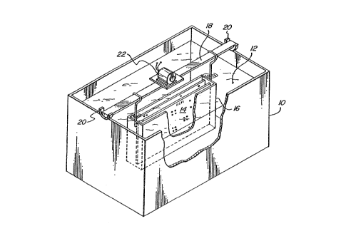
BRIEF DESCRIPTION OF THE DR~WINGS
FIG. 1 is a schematic perspective illustration of
an electroless platin~ vessel having substrates, held in
a rac~, ir~mersed in an electroless plating bath in the
vessel, and in which a vibratory device is affixed to the
flight bar on which the rack is suspended.
FIG. 2 is a schematic perspective illus~ration o~
an electroless plating vessel havi~g substrates, held in
a rack, immersed in an electroless plating bath in the
vessel, and in which a vibratory device is affixed to a
support bar on which rests a carrier bar on which the
rack is arranged.
DETAILED DESCRIPTION OF THE INVEN~ION
The present invention is particularly applicable
to the electroless plating of copper (again, used here to
include copper metal, copper alloys or copper inter-
rnetallic~ on any suitably activated substrate surface,
,,; :
including substrates composed of thermoplastic or thermo-
set~ing materials, glass, ceramics, and the like. The
invention is particularly applicable, as noted, to
electroless plating employed in the fabrication of
printed circuit boards, where the substrates commonly
encountered are based upon epoxy or polyimide, parti-
cularly glass reinforced versions thereof. The invention
is primarily applicable to the electroless plating of
activated through-hole surfaces in double-sided or multi-
layer printed circuit boards. As noted, the invention
has particular applicability to the electroless plating
of through-holes having high aspect ratios, e.g~, greater
than 3:1 and generally greater than 8:1, but also has
been found to brin~ about substantial improvement in the
plating of low aspect ratio through-holes (e.g., 3:1 and
less) which heretofore have been considered satis-
factorily processable using conventional electroless
plating techniques.
The surfaces to be electrolessly plated with
copper will be treated in conventional m~nner to clean
the surfaces and provide thereon species which catalyze
the electroless deposition, all as previously noted. For
through-holes, particularly those in multilayer circuit
board substrates, the hole surfaces will be subjec~ed to
conventional surface preparation steps for desmearing
and/or etchh~ck, conditioning, and the like, preparatory
to catalytic activation and electroless plating.
The electroless plating baths can be any of the
known baths for electroless deposition of copper, in
cluding formaldehyde-reduced baths, and hypophosphite-
reduced baths. As is known in the art, many
hypophosphite-reduced copper plating baths are generally
non-autocatalytic and, thus, cannot alone produce the
plating thicknesses necessary in ~ull-build applications
-10--
(e.g., greater than 1.0 mil). Thus, in the preferred
full-build applications, either formaldehyde-reduced
electroless copper plating baths will be employed or
hypophosphite-reduced baths which have been modified, or
are used in a manner, which renders them autocatalytic
~ and hence capable of attaining the requisite plating
thicknesses. See, e.g., U.S. Patent No. 4,265,943 to
Goldstein, et al.; U.S. Patent No. 4,459,1B4 to
Kukanskis; and U.S. Patent No. 4,671,968 to Slominski.
10 Where full-build thicknesses are not re~uired, use can be
made of the non-autocatalytic hypophosphite-reduced
copper baths as disclosed in Kukanskis, et al. U.S.
Patent Nos. 4,209,331 and 4,279,948.
As set forth in FIG. 1 and FIG. 2, a typical
15 electroless plating vessel or tank 10 is used to house
the electroless plating bath 12, and typically will have
means associated therewith for agitating the plating
bath, recirculating overflow bath, and maintaining the
bath at suitable operating temperature, typically in
20 excess of about 120~F and more typically in the range of
from abou~ 130~F to 150~F.
Through-hole containing substrates 14 are suspend-
ed in the electroless plating bath from racking device 16
which holds the substrates in parallel and in generally
25 vertical orientation in the electroless bath.
In the embodiment of FIG. 1, the racking device 16
is suspended from a flight bar 18 which extends across
the plating vessel 10 and rests on the upper walls of the
vessel, most preferably resting on saddles 20 affixed to
30 the tank walls.
According to this embodiment of the invention,
vibratory device 22 is affixed to the flight bar 18,
~, .. ..
e.g., magnetically or otherwise, and is in turn connected
to an electrical source (not shown) for driving the
vibratory device. The vibratory device affixed to the
flight bar transmits vibrations to the rack and in turn
to the substrates held in the rack, causing them to
vibrate in contact with the plating bath. As noted, the
vibratory device typically will be operated at generally
regular on-off periods during the electrol~ss depositing
process so as to at least intermittently subject the
lo substrates to the vibrating necessary to produce electro-
less deposits of improved overall inte~rity, particularly
resistance to cracking.
In the embodiment of FIG. 2, the racking device 16
also is suspended into the plating vessel from a flight
or carrier bar 18. In this embodiment, support bars 24,
having saddles 20 affixed thereto, are a~fixed to rims or
flanges 26 associated with the plating tank walls. The
carrier bar 18 is arranged to rest on the saddles 20 of
these suppor~ ~ars 24, and vibratory device 22 is affixed
to at lea3t one of the support baxs. Preferably, the
support bars 24 and/or the tank r:ims 26 include coil
springs 28 which are put into compression when the
suppor~ bar is affixed to the tan3~ rim. The vibratory
device 22 transmits vibrations to the support bar 24, in
2S turn to carrier bar 18, in turn to racking device 16, and
in turn to the substrates 14 held in the racking device.
The in~ention is illustrated further in the
following examples.
EXAMPLE I
A multilayer epoxy-glass circuit board having a
board thickness of 125 mils and through-holes 8 mils in
diameter (i.e., aspect ratio of about 16:1) was prepared
:~ 2 ~
-12-
ror additive electroless plating by subjectin~ the board
i: and through-holes to steps of solvent conditioning,
permanganate desmear, conditioning, activation and
. acceleration. The so-prepared substrate, held in a con-
ventional rack suspended from a flight bar, was immersed
in vertical orientation in an electroless copper plating
bath containing cupric salt (2.0 g/l based on cupric
ion), complexing agent (0.1 Molar), formaldehyde (2.0
gll), caustic (3.0 g/l) and stabilizers (5.0 ppm), and
operated at 140~F for 20 hours to achieve a plating
thickness of 1.4 mils.
~ A vibrator (Martin Micro Motomagnetic~ Electric
Vibrator (3600 RPM, 115 volt, 60Hz), Martin Engineerin~
Company, Neoponset, Illinois) was attached to the flight
bar (configuration as in FIG. 1), and during the 20-hour
plating process was operated at 60 seconds on, 120
seconds o~f.
During this time, the rack also was subjected ta
slow mechanical back and forth movement at a rate of 2
feet pex minute.
After plating, the board was dried and baked for 4
to 6 hours at 300~F, and sections of the board were then
tested as follows. The plated through-holes were floated
on molten solder at 500~F for 10 seconds, allowed to cool
to room temperature, and then reimmersed in the molten
solder, a se~uence repeated five times. Other through-
holes were immersed in hot oil at 550~F for 20 seconds,
allowed to cool in room temperature oil for 2 minutes,
and then reimmexsed in the hot oil, a sequence repeated
20 times. The so-treated through-holes were then cross-
sectioned and examined under a microscope, with no
evidence of cracking of the plated deposit found.
: . ~., '
2~2~
EXAMPLE II
Example I was repeated in all respects but without
the use of the vibratory device, resulting in a 1.2 mil
plate after 20 hours. After the solder and hot oil
s testing, microscopic ~mi ~ation revealed cracking of the
copper deposit.
EXAMPLE III
Example II was repeated with the exception that
plating was continued until a deposit of 1.4 mils was
obtained. Again after testing, ~mination of the copper
deposit revealed cracks~ thus d~monstrating that the
results of Example II were not related to the thickness
of the deposit.
EXAMPLE IV
Two multilayer circuit boatds having 2~ mil --
through-holes (aspect ratio 3:1) were identically
prepared and additively plated as in Example I for 20
hours to a copper plating thickness of 1.3 mils, one
board being plated using the vibratory device oi Example
I and the other board plated with just the mechanical
back and forth movement of the rack. The boards were
then dried, baked and subjected to the te~ts set forth in
Example I, with the exception that, in order to determine
at what stage cracking occurred, a portion of the board
was cross-sectioned after every two cycles. After two
cycles, through-holes sectioned from each board revealed
no cracks. After four cycles, the through-hole from the
non-vi~rated board showed evidence of the beginning of a
crack propagating from the shoulder of the hole, while
the board plated with vibration showed no such cracking.
After six c~cles, the non-vibrated board showed complete
202~
-14-
cracking of the copper deposit, while the other ~oard
showed no cracking. Testing continued for the board
plated with vibration until 20 cycles, at which point a
crack was beginning to form.
As is known in the art, through-holes with aspec~
ratios of 3:1 are suf~iciently large that, with routine
bath agitation and gross mechanical back and forth
movement of the substrate, solution flow through the hole
and solution exchange with the hole are easily accomplish-
ed and not a limiting factor in attaining good electro- .
less plating. Accordingly, the significantly improved
results attained with the vibration of the invention are
apparently not attributable simply to increased solution
~x~h~nge.
As will be apparent from the foregoing descrip-
tion, the process of the present invention, although
described with particular regard to the electroless
copper plating which is of primary interest in the - :
fabrication of printed circuit boards cont~ining through-
holes, also has applicability to t:he electroless plating
of other metals, alloys or intermetallics, such as
nickel, gold, and the like. So too, the vibrating
process also can be applied with advantage to other
processes in which substrates are immersed in solutions,
2s including all the various surface pre~aration processes
employed preparatory to electroless plating, including
cleaning, conditioning, ~e~P~ring~ etch-~ack, activa-
tion, acceleration, and the like, as well as post-
electroless deposition processes, particularly where high
aspect ratio through-holes are present.
The foregoing description, then, is presented to
describe and illustrate the invention and its preferred
embodiments, and is not to be taken as limiting the
invention whose scope is defined in the appended claims.
'