Note: Descriptions are shown in the official language in which they were submitted.
2 ~
APPARATUS AND METHOD FOR INSTALI~TION
OF MULTI-PIN COMPONENTS ON CIRCUIT BOARDS
Backaround of the Inventio~
The invention relates to a converter socket ~or
connecting a multiple pin component to a plurality of
sockets attached to a circuit board.
For a variety of reasons, manufacturers of
electronic circuit boards use sockets as a means for
connecting integrated circuits (Ics) to a circuit ~oard.
However, Ics are more commonly soldered directly to the
printed circuit board (PCB). Each pin of. the IC is inserted
into a plated through hole in the PCB. Solder is then
applied to electrically connect the pin to the walls of the
plated through hole. Since the solder will provide an
electrical connection even if the pin is thin relative to
the hole diameter, manufacturers of ICs typical}y do not
control the dimensions of the pins to a high degree of
precision. Rather, to reduce costs, a manufacturing process
is used which yields pins having dimen5ions which vary over
a wide range ~i.e., a coarse tolerance).
Accordingly, conventional circuit board sockets are
designed to accommodate pins having a wide range of
diameters (i.e., pins having a coarse tolerance~. In order
to accommodate pins of relatively narrow diameters, these
2S sockets tend to engage the relatively wide pins with a
degree o~ friction which far exceeds that required to yield
the desired electrical contact. As a result, the aggregate
frictional forces caused by the engagement of a large number
of IC pins with their companion sockets can be sufficiently
large to require the use of specialized tools to assist in
extracting and inserting the IC.
Summary of the Invention
In general, in one aspect, the invention features
effectively reducing the wide variation in pin diameter
(i.e., coarse t~lerance) of a multi-pin component by
introducing converter elements between the component and the
board mounted sockets. The converter elements accept ~he
coarse tolerance pins of the component, and provide in their
place precision tolerance pins ~i.e., pins with a diameter
tolerance less than the coarse tolerance of the component
pins) for insertion into the board-mounted sockets.
Preferred embodiments inclu~e the following
features. The receptors are sized and positioned on the
body to engage pins having pin spacing and pin diameters
each of which vary within coarse ranges. The precision pins
are controlled such that the pin spacing and pin diameters
are each within precision ranges, the variation within the
precision ranges being less than the variation within the
coarse ranges. For example, the precision variation of pin
spacings is 0.004 inches or less, while the coarse variation
is 0.01 inches or greater. Similarly, the precision
variation of diameters is 0.001 inches or less while the
course variation of diameters is 0.004 inches or greater.
Further the body includes an opening positioned
beneath the component when the component is installed in the !;~
sockets. The opening is sufficiently large to accommodate a
knockout of an extraction tool to engage the bottom o~ the
multi-pin component to provide an extraction force between
the body and the component.
In general " n another aspect, the in~ention
features making connections between the pins of a multi-pin
component and posts mounted on a circuit board. The
invention includes converter elements having a first
receptor for mating with a pin of the mult.lple pin
. :.
component, and a second receptor for mating with a post on
the circuit board.
In general, in another aspect, the invention
features a contact stub having a curved end for making
S connection with the resilient fingers of a socket mounted on
a circuit board. The length of the stub is sufficiently
short so that when the stub is fully inserted, the finger~
engage the curved end of the stub to provicle a force with an
upward component, i.e., a component parallel to the
longitudinal axis of the stub, and in the direction
resisting insertion of the stub.
The invention provides several advantages. For
example, since the dimensions of the pins of the converter
elements are precisely controlled, the force required to
15 remove the precision pins from the board mounted sockets is ;
substantially reduced. Accordingly, by mounting the multi-
pin component to the board via the converter elements, the
multi-pin component can be removed with reduced force,
thereby lessening the mechanical strain on the body of the
component. Further, in embodiments wherein the converter
elements include contact stubs having curved ends, the force
of removal may be reduced to zero.
Converter elements having a pair of receptors allow
component pins to be connected to board mounted posts. This
allows board mounted posts to be used in lieu o board
mounted sockets. Since the posts cover less surface area of
the board than the soc~ets, additional board area is freed
for use in running conductive etches.
Other ~eatures and advantages of the invention will
be apparent from the following description ~ the preferred
embodiments and from the claims.
; . . , . ,. i . .. , ,. ~ ... ~ .. - . .. ,1 . , .; . ,
2~¢~
- 4 -
Description of the Preferred Embodiments
Fig. 1 is a side view of a prior art pin grid array
in position to be installed in sockets of a printed circuit
board.
Fig. 2 is a cross-sectional view at 2~2 of Fig. 1.
Fig. 3 is a perspective view of a prior art socket
contact.
Fig. 4 is a side view of a preferred embodiment of
the invention.
Fig. 5 is a cross-sectional view at 5-5 of Fig. 4. ;
Fig. 6 is a cross-sectional view along the same
section as Fig. 5, showing the parts assembled.
Figs. 7-8 are cross-sectional side views, showing
another preferred embodiment. !~
Figs. 9-10 are perspective views of a prior art
socket sleeve.
Fig. 11 is a cross-sectional view of an extraction
~ack screw.
Fiq. 12 is a cross-sectional view of another
preferred embodiment.
Figs. 13 is a cross-sectional view of a segment of
~he embodiment shown in Fig. 12, with the converter socket
p~rtially installed in the circuit board sockets.
Fig 13a is a more detailed view o~ region A of Fig.
13.
Fig.14 is a cross-sectional view of a segment of the
embodiment shown in Fig. 12, with the converter socket fully
installed in the circuit board sockets.
Fig 14a i~ a more detailed view of region A of Fig.
30 14. ;
A conventional socket installation of an IC in a
circuit board is shown in Figs. 1 and 2. An IC having a -
large number of pins is often packaged as a pin grid array
,. " .-
;`'`~ ' ',
' i ; .
"'
2 ~
(PGA) 10. PGA 10 includes a ceramic body 12 which supportsa group of male contact pins 14. Typically, pins 14 are
manufactured with diameters Dl which vary over a relatively
co~rse range. For example, diameters may vary from 0.016 to
0.020 inches (i.e., a variation of 0.004 inches). Thus, the
largest diameter pin (0.020 inches) can be 25 percent larger
than the narrowast diameter (0.016 inches).
Similarly, the distance D2 between pins ( Fig. 2)
may vary over a relatively coarse range. For example,
adjacent pins are typically 0.1 inches apart but may vary
from the typical separation distance by up to +0.005 inches
(i.e., a variation of 0.010 inches) from tip to tip.
~ PGA 10 is often mounted to a printed circuit board - -
(PCB) 16 by inserting each pin 14 of the PGA into a
corresponding socket 18 which is soldered into a plated
through hole of the printed circuit board. The body 20 of
the socket is soldered to the PCB. A contact 22 is pressed
in~o the interior of the body. The contact frictionally
engages the sides of each pin 14. As shown in Fig. 3,
contact 22 includes a barrel 24 attached to a plurality of
spring elements 26. Pin 14 passes throùgh the barrel and
frictionally engageC spring elements 26 to form an
electrical connection. Several pins 14 include standoffs 15
which engage the top of the socket when the PGA is fully
inserted.
The spring elements are designed to engage pins
having any diameter within the coarse range of PGA pin
diameters. The largest pin diameter which the spring
elements can accommodate is determined by the elastic limit
of the spring elements. If a pin having a greater diameter
is inserted into the socket, the spring elements will
experience plastic deformation such that on removal of the
.
':
.. . , . .. . . ~ ,. ., . . .. . ~ . . . .
- 6 -
pin, the spring elements will not return to their original
position.
~- The smallest diameter which the spring elements can
accommodate is determined by the minimum normal force
between spring elements and pin required to achieve a
reliable electrical contact. For example each spring
element should engage the pin with at least 15 to 50 grams
of normal force and preferably 25 grams.
To assure a reliab~e connection, sprinq elements 26
must be designed to provide sufficient frictional engagement
with even the narrowest possible pin 14 (i.e. 0.016 inch
diameter). Accordingly, most socket designs provide an even
greater frictional engagement with larger pins. -
The frictional engagement between a pin and its
socket may be yet further increased if the pin and an
ad~acent pin are ~urther apart or closer together tllan their
companion sockets. Such a disparity, which results in part
from the coarse range of PGA pin spacinq, may force each pin
against one side of its companion socket, thereby
substantially increasing the frictional engagement.
As explained in J.B. Cullinane, "Pin Grid Array
; Socket Total Forces", 22nd Annual Connector &
; Interconnection Technology Symposium (1989) (incorporated
herein by reference) other variables which contribute to the
; ~5 total insertion/extraction forces include: pin length, end
of pin geometry, cumulative pin to pin tolerance, pin true
positioning pin perpendicularity, pin material and pin
plating composition.
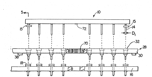
A preferred embodiment of the invention is shown in
Figs. 4-6. A converter socket 28 having a body 30 holds a ~-
pl~rality of converter elements 32, arranqed in the same
footprint as PGA 10. Each converter element 32 includes a
female socket 34 for mating with a corresponding PGA pin 14,
' '":
,
:
.
~ '3
and a high precision pin 36 for mating with PCB socket 18.
The dimensions and reiative locations of pins 36 are tightly
controlled to eliminate the increased frictional engagement
forces described above. For example, the dlistance between
adjacent pins is controlled to within 0.002 inches of the
typical distance, 0.1 inches. Further, each pin diameter D3
is controlled ts within ~ 0.0005 inches of the typical
diameter, 0.0165 inches (i.e., a variation of 0.001 inches).
When used with conventional sockets 18, the pins 36
can be designed with a diameter corresponding to the
narrowest diameter which the socket can accommodate, thereby
minimizing the frictional engagement.
This invention also makes possible the use of
nonconventional printed circuit board sockets specifically
designed to take advantage of the precision of pins 36, to
reduce the force of frictional engagement. For example,
Figs. 9 and 10 depict a prlor art socket sleeve 60 ~or
mating with precision pin 62. Socket sleeve 60 provides an
electrical contact with pin 62 with little frictional
engagement. However, to use this type of sleeve, the
inserted pin 62 must be manufactured with a relatively hiyh
degree of precision. For example, sleeves 60 designed to
accommodate pins 62 having a diameter of 0.018 inches,
typically require that the pin be within 0.0004 inches of
that diameter.
While the use of precision pins 36 reduces the
frictional engagement with soclcets 18, the frictional
engagement between the PGA pins 14 and female sockets 34 may
remain sufficient}y great (in cases where a great many pins
extend from the PGA) to require the assistance o~ an
extraction tool to separate the PGA from the converter
socket. Toward thls end, a threaded pem nut 70 may be
.~ ;,','~.'.
- ~ _
pressed into an opening in the center of the body 30 of the
converter socXet. Many PGAs, as shown in Fig. 4, include a
desert region 72 near the center of the body of the PGA
having no pins. Accordingly, to separate PGA 10 from
converter socket 28, a threaded jack screw 74 (Fig. 11) may
be employed. Jack screw 74 includes a thr~eaded post 76 for
mating with pem nut 70. As the jack screw is threaded into
the pem nut, the end 78 of the threaded post serves as a
knockout means, by engaging the bottom of the PGA to
separate the PGA from the converter socket. To provide
leverage, ~he jack screw includes a gripping knob 80 having
a diameter greater than that of the threaded post.
Another preferred embodiment is shown in Figs. 7-8.
A converter socket 40 provides a connection between the pins
of PGA 10 and posts 42 mounted on printed circuit board 44.
In this embodiment, the converter element 46 includes a pair
of female sockets 48,50 for mating with post 42 and pin }4
respectfully .
The ability to install a PGA using board mounted
posts instead of sockets can facilitate the use of
; conductive etches during manufacturinq. Posts 42 typically
have smaller diameters than sockets 18 and accordingly cover
less area o~ the top surface 52 of PCB 44. Even with 0.1
inch spacing between posts as re~uired for conventional
PGAs, sufficient space is available to allow conductive
etches to run between adjacent posts 42. Sockets, with
their wider profiles, often operate as a virtual wall to the
running of etch, thereby complicating layouts of the printed
circuit board.
To achieve reduced friction, PCB posts 42 and female
sockets 48 are manufactured and positioned with the same
precision as posts 36 (Fig. 5~. Accordingly, converter-
socket 40 provides the dual advantage o expanding the `
.;-
:,.
$ t 3
amount of PCB surface available for running etches and
facilitating insertion and extraction of the PGA.
In another preferred embodiment shown in Figs. 12-
14, extraction forces are rPduced practically to zero. In
this embodiment, each converter element 132 of converter
socket 128 includes a female sock~t 134, ildentical to socket
34 (Fig. 4) described above, for mating with a corresponding
PGA pin. However, ~or mating with PCB socket 118, converter
element 132 lncludes a short contact stub 136 havin~ a
lo curved end 138.
The contact stub engages with fingers, or spring
elements, 126 of socket 118 to form the desired electrical
connection. The dimensions of the contact stub are chosen
to prevent the fingers, or spring elements, from gripping
the stub in a manner which resists removal. During
insertion, region B1 of the contact stub P~rst contacts each
spring element in a region Al. With further insertion, the
contact stub wipes across the surface of the spring element,
pushing the elements apart. When fully inserted, stop 137
rests on the surface of PCB 116 and region B2 of the stub is
press~d against region A2 of each spring element. The
dimensions of the stub, the spring elements, and the stop
are chosen such that B2 lies on the curved surface of the
stub, and such that the distance ~ between Al and A2 is
sufficiently large that adequate wiping action occurs to
remove oxide build up on the contact regions (ie. ~ = 0.010
-0.015).
The contour of the curved surface is chosen to
ensure that~ even in the fully installed position, spring
elements 126 push on the stub with a force having a
vertically directed component. The aggregate o~ the
vertical Porces on the stubs is suffici-nt to eject the
,,',. :"
' '.
2 ~
- 10 -
converter socket/PGA assembly unless a counterbalancing
force holds the assembly in place. Toward this end, a pull
down screw 172 is employed to mate with pem nut 170 to pull
the converter socket/PGA assembly into the fully inserted
position and hold it in place. In this embodiment, the pem
nut serves dual purposes. When used with pull down screw
172, it assists in maintaining contact between the stubs 132
and spring elements 126. When used with jack screw 74 ~Fig.
11) it assists in separating the PGA from the converter
socket.
Other embodiments are within the following claims. -
For example, the invention can be applied to a variety of
different board-mounted sockets, including sockets
consisting solely of contacts pressed into holes in the
circuit board. The connection technique of Figs. 12~}4
could be applied to the direct connection of a PGA to the
circuit board if the preferred contact stubs 136 were
provided on the PG~. `
What is claimed is: