Note: Descriptions are shown in the official language in which they were submitted.
RCA 85.616A 2~2~4
AN ADAPIIVE
~IULl~STANDARD VlDEO COMB FILTER
This invention is related to comb filters for processing
video signals.
In processing video signals, it is known to be
particularly advantageous to sgparate the luminance and
chrominance components from composite video signal with comb
filters. The reason being that the separated luminance component
is of full bandwidth, e.g., 4.2 MHz for NTSC signal, and cross
components are substantially eliminated from both of the
separated luminance and chrominance components. Typical
intraframe comb filters for NTSC video signals include circuitry for
combining signals which are displaced in time by an odd integral
number of horizontal line periods. Because the phase of the
chrominance subcarrier changes by exactly 1 80 from line to line,
additively combining .~TSC video signals displaced by one line
interval produces a signal in which the luminance components
from the two lines constructively combine and the chrominance
component is cancelled. Conversely, if the signals are
2 0 subtractively combined the luminance component is cancelled
while the chrominance components from the two lines
constructively combine. The vertical resolution of the luminance
component is compromised but is acceptable.
PAL signals on the other hand have a chrominance
2 5 subcarrier which exhibits a 180 phase change every two
horizontal line periods. Therefore, typical intrafrarne PAL comb
filters combine video signals which are displaced in time by two
horizontal intervals. The PAL comb filter function is basically the
same as for the ~TSC comb filter however, since the signals that
3 0 are combined are spatially displaced by two lines, the vertical
resolution of the PAL lllminance component is significantly
impaired, and tends towards not being acceptable.
Yoshimitsu Nakajima et al in an article entitled
"Improvement of Picture Quality for NTSC and P~L Systems by
Digital Signal Processing", IEEE Transactions on Consumer
Electronics, Vol. CE-31. No. 4, Nov. 1989, pp. 642-654 describe
adaptive comb filters which combine samples from three
successive lines of video signal. In this system, the ~TSC
RCA 85,616A 2029554
embodiment combines samples which are vertically aligned,
similar to the aforedescribed typical NTSC and PAL comb filters.
The PAL embodiment however combines diagonally aligned
samples from adjacent lines. This tends to preserve the vertical
5 resolution of the luminance component, reduces memory
requirements for delaying the video signals but tends to have an
adverse affect on images containing vertical lines.
Simple comb filters tend to introduce cross
components in the separated luminance and chrominance signals
10 where differences exist in the composite signal line-to-line. It is
known, however, that such cross components may be significantly
reduced by the process of adaptive comb filtering. Examples of
adaptive comb filters may be found in U.S. Patent No. 4,786,963
- issued to McNeely et al. and U.S. Patent No. 4,803,5~7 issued to
15 Stratton. In adaptive systems, signals from a plurality of adjacent
lines are provided. These signals are compared to determine
which signals, when combined to provide a comb filter output, will
tend to produce the most desirable signal.
In order to realize economies of scale in the
2 0 manufacture of video signal processing components it is
advantageous to produce multistandard processing elements
which are useful for, e.g., NTSC and PAL signal systems. To this
end it is desirable to have a multistandard comb filter. Shinichi
Nakagawa et al. in United States Patent No. 4,727,415 describe an
2 5 adaptive multistandard comb filter system. In this system, for
the NTSC mode, the comb filter adaptively combines composite
video samples from adjacent lines of video signal, to produce
separated luminance and chrominance components. In the PAL
mode, the comb filter adaptively combines composite video
3 0 samples displaced by two horizontal lines to produce separate
luminance and chrominance components. As such, in the PAL
mode, there is a loss of vertical resolution.
This invention is directed toward circuitry for
generating control signals for an adaptive multistandard comb
3 5 filter which generates alternative comb filtered signals
representing a particular horizontal line from video signal samples
representing at least first, second and third horizontal lines. A
first circuit means generates a first plurality of sums of samples
RCA 85.616A 2a23~5~
from said first and second horizontal lines and a second plurality
of sample sums from said second and third horizontal lines, and
generates a first plurality of differences of samples from said first
and second horizontal lines and a second plurality of differences
5 of samples from said second and third horizontal lines. A second
circuit means, generates said control signal responsive to said first
and second pluralities of sample sums in said first mode, and
generates said control signal responsive to ones of said sums of
said first and second pluralities of sample sums and ones of said
10 differences of said first and second pluralities of differences in
said second mode.
FIGURES 1 and 2 are pictorial representations of video
samples from portions of three horizontal video lines for NTSC and
PAL signals respectively.
FIGURES 3 and 4 are block diagrams of alternative
multistandard adaptive comb filters embodying the present
invention.
FIGURE 4A is a block diagram of circuitry which may
be included in the FIGURE 4 circuitry to proportionally provide
O alternative luminance signal.
FIGURE 5 is a block diagram of an exemplary
switchable bandpass filter which may be utilized for elements 26,
28 and 30 in the FIGURES 3 and 4 apparatus.
FIGURE 6 is a block diagram of circuitry for providing
2 5 a plurality of relatively delayed sum and difference signals.
FIGURE 7 is a block diagram of circuitry for providing
a control signal K for adaptively controlling the circuit element 63
in FIGURE 4.
FIGURE 8 is a block diagram of circuitry for providing
3 0 a control signal Kch, for controlling the circuit element 65 of
FIGURE 4.
FIGURE 9 is a block diagram of circuitry for providing
a control signal KL, for controlling the circuit element 74 of
FIGURE 4A.
FIGURE 10 is a block diagram of circuitry for
producing an alternative luminance signal.
The invention will be generally described in terms of
digital processing hardware operating on a digitized (PCM) video
RCA 85,616A 2029~54
signal, however, it will be appreciated that the invention may be
practiced on either analog or digital video signals with appropriate
selection of circuit elements.
Referring to FIGURE 1 the array of circles represent
5 samples of an NTSC video signal from portions of three adjacent
horizontal lines. The samples are presumed to have been taken at
a rate of four times the color subcarrier frequency with a
sampling signal phase locked to the I or Q axis (I and Q being
quadrature phase color difference signal components). The
10 darkened or filled circle represents the sample point for which a
comb filtered signal is to be currently generated. Since the
samples occur at a rate of four times subcarrier and phase locked
to the I or Q axis each sample contains I or Q color information
exclusively. Note if the applied signal includes a luminance as
15 well as a chrominance component, respective samples may be
represented Y+I or Y+Q where Y represents luminance
information. To avoid confusion the Y terrns have been omitted in
FIGURES 1 and 2.
Because of the aforedescribed sampling method,
2 0 vertically aligned samples contain like chrominance components.
The phase of vertically adjacent samples is however reversed.
Assume that samples a, b and c have equal values (Y-I)a, (y+I)b
and (Y-I)C respectively. Subtracting sample a from sample b will
produce the sample +2I which represents a comb filtered
2 5 chrominance component of proper phase. Similarly subtracting
sample c from sample b will produce the sample value +2I. To
generate a comb filtered sample representing sample point b in
line N, the corresponding vertically aligned sample from either
line N+1 or line N-1 may be combined with sample b. The method
3 0 for selecting the sample to combine with sample b will be
discussed hereinafter. Note in ~IGURE 1 the dark arrows
designated 3 and 8 indicate the pairs of samples which may be
combined to generate the comb filtered sample representing point
(pixel) b. Similarly, the broken arrows indicate pairs of samples
3 5 which may be combined to produce comb filtered samples for
respective samples along line N. The numbers 1-10 adjacent the
respective arrows designate pairs of samples that are used in ~he
adaptive comb filter process, which pairs of samples will be
RCA 85 ,61 6A
referred to in the description of FIGURES 6-10. For example.
sample pair 3 consists of samples a and b and pair 8 consists of
samples b and c.
FIGURE 2 is a representation of samples from a portion
5 of four lines of a PAL video signal. The PAL signal samples are
also presumed to be taken at a-rate of four times the color
subcarrier frequency. The solid circle represents the pixel
location for which the video signal is currently being processed. U
and V represent quadrature phase color difference signals. In this
10 instance the sampling signal is phase locked to the color
subcarrier at an angle 45 off the U color difference signal axis.
As a result the chrominance component at each sample instance
includes a contribution from both color difference signals rather
than exclusively one or the other of the color difference signals. It
15 is seen however that the values of every second pair of samples
between adjacent lines represent like chrominance components
with a 180 phase relationship, e.g., pairs 1, 3, 5, 7, etc. A comb
filtered chrominance component for sample point or pixel b may
be provided by subtractively combining samples a and b. A comb
2 0 filtered chrominance component for each of the five pixels in line
N, starting from left to right may be provided by subtractively
combining the sample pairs 1, 7, 3, 9 and 5 respectively. A comb
filtered signal of this type is herein defined as a line alternating
subtractive comb filtered signal or LASCFS. If the signal
25 represented by the samples of FIGURE 2 is composite video this
comb filtering process will substantially eliminate the luminance
component except where there are line-to-line amplitude
variations.
Unlike the NTSC case, vertically opposite pairs of
3 0 samples are not conducive to subtractive comb filtering because
the samples are of like chrominance phase. For example, the pair
of samples 8 opposite pair 3 are of the same phase, e.g., +(V-U).
Thus, if the comb filtered signal produced by subtractively
combining the pair 3 samples is likely to introduce an artifact, one
3 5 cannot simply select a sample representing the subtractively
combined sample representing pair 8 as a substitute signal.
Nominally the energy content of the luminance
component within the frequency spectrum occupied by the
RCA 85.616A
chrominance component is small. Therefore, if the signal
represented by the array of samples of FIGURE 2 occupies only
the chrominance frequency band, the alternate pairs of samples
(e.g., 6, 2, 8, 4 and 10) may be additively combined to provide a
substitute chrominance signal. A sequence of samples
representing the additive com~ination of alternating sample pairs
6, 2, 8, 4 and 10 is herein defined as a line alternating additive
comb filtered signal or LAAC~FS. This signal will include the low
energy high frequency luminance component. However,
depending on the potential error in the subtractive comb filtered
signal, it may still be advantageous to substitute the additive
comb filtered signal even though it does include some luminance
signal.
- As in the NTSC case, the relative amplitudes of the
respective PAL samples may be monitored to adaptively select
which of the LASCFS or LAACFS is to be provided as output signal.
Desirably this will be accomplished with a high degree of
commonality in the processing hardware for both the NTSC mode
of operation and the PAL mode of operation.
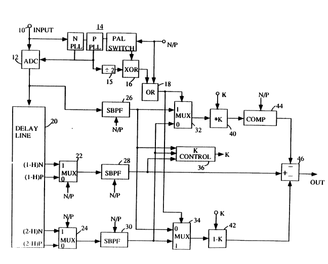
Refer now to FIGURE 3 which illustrates a first
embodiment of an adaptive NTSC/PAL comb filter arranged to
provide a comb fil~ered chrominance output signal. Input analog
signal which may be a chrominance signal modulating a
subcarrier/carrier or composite video having characteristic of
either the NTSC standard or the PAL standard is applied at
terminal 10 to an analog-to-digital converter (ADC) 12, and to a
sampling signal generator 14. Sampling signal generator 14,
responsive to a signal N/P, which may be provided by a user
operated switch or an automatic standard detector (not shown)
3 0 develops a sampling signal having a frequency of four times the
subcarrier frequency. Generator 14 may include NTSC (N PLL)
and PAL (P PLL) phase locked loops, which are respectively
selected by the signal N/P, and are responsive to the subcarrier,
for generating the sampling signal. The N-PLL develops a
3 5 sampling signal which is norninally phase aligned to one of the
quadrature axes of the subcarrier. The P-PLL develops a
sampling signal which is phase aligned 45 from one of the
quadrature axes of the subcarrier. In addition the generator 14
RCA 85~616A 2023~a4
includes circuitry for generating a PAL switching signal which is
logically high during alternate horizontal line periods and logically
low during intervening horizontal line periods. The frequency of
the sampling signal is divided by two in divider 15 and applied to
5 one input of an exclusive OR (XOR) gate 16. The PAL swi~ching
signal is applied to a second input of the XOR gate. The output of
the XOR gate 16 is a signal, synchronous with the sampling signal
but of half the rate of the sampling signal, and which is of
opposite phase line-to-line. This signal is utilized in the PAL
10 mode to select alternate samples along a horizontal line. The
signal from the XOR gate 16 and the control signal N/P are coupled
to respective input terminals of an OR gate 18. In this and the
following examples the control signal N/P is presumed to exhibit
logic one and logic zero states for the NTSC and PAL modes of
15 operation respectively. Therefore, OR gate 18 exhibit~ a logic one
output in the NTSC mode and passes the signal provided by the
XOR gate 16 in the PAL mode of operation.
The ADC 12, responsive to the sampling signal from
generator 14, produces pulse code modulated (PCM), e.g., binary,
2 0 representations of the input signal at a sample rate of four times
the subcarrier. The PCM sarnples are applied to a delay line 20
having taps for providing signals delayed by one and two
horizontal line intervals for NTSC signals and for PAL signals, (910
and 1 820 sample periods for NTSC and 11 35 and 2270 sample
25 periods for PAL). The (1-H) NTSC and PAL taps are coupled to a
first multiplexer 22 and the (2-H) NTSC and PAL taps are coupled
to a second multiplexer 24. Multiplexers 22 and 24 are
responsive to the control signal N/P to provide delayed samples
from the appropriate taps for the NTSC or PAL operating modes.
3 0 Input samples applied to the delay line 20 and delayed samples
from multiplexers 22 and 24 respectively correspond to vertically
aligned samples ~rom three adjacent video lines as exemplified by
samples c, b and a in FIGURES 1 and 2.
The signal samples provided by the ADC 12 and
3 5 multiplexers 22 and 24 are coupled to switchable bandpass filters
(SBPF) 26, 28 and 30, respectively. Bandpass filters 26, 28 and 30
only pass signal in the frequency band normally occupied by the
chrominance signal, and are responsive to the control signal N/P
RCA 85'616A 20~9~5~
to select the appropriate NTSC or PAL chrominance frequency
band. FIGURE 5 illustrates an exemplary SBPF which may be used
for filters 26, 28 and 30. This is a straight forward design and
will not be described in detail. The blocks labeled 2T are delay
5 elements for delaying samples by two sample periods. The blocks
labeled with a decimal number- are weighting circuits for scaling
the value of the samples by the respective decimal factor. It is to
be noted that the FIGURE 5 filter arrangement includes both a low
pass output (LPF) and a bandpass output (BPF). The BPF output
1 0 provides the samples which are combined to forrn the comb
filtered signals. The LPF output is utilized in the adaptive control
clrcultry .
Referring again to FIGURE 3, the BPF output from the
SBPF filters 26 and 28 are each coupled to respective input
1 5 terminals of two multiplexers 32 and 34. l~he output of the SBPF
28 is coupled to a first input of a combining circuit 46. The output
of multiplexer 32 is coupled to a second input of the combining
circuit 46 via a scaling circuit 40 and a polarity inverting circuit
44, and the output of multiplexer 34 is coupled to a third input of
20 the combining circuit 46 via a scaling circuit 42. Scaling circuits
40 and 42 are responsive to a control signal K for scaling sample
values by K and 1-K respectively, where K is nominally equal to
values between 0 and 1 inclusive. The values of K are provided
by the adaptive K control circuit 36 which is responsive to signal
2 5 provided by the filters 26-28. The polarity inverting circuit is
responsive to the mode control signal N/P to pass samples
unaltered in the NTSC mode and to complement samples in the
PAL mode.
In the NTSC mode of operation the multiplexers 32
30 and 34 are conditioned by the signal provided by OR gate 18 to
respectively pass samples provided by SBPF 26 and SBPF 30.
Refer to FIGURE 1 and consider pixel b. The desired comb filtered
outpue is (b-a) or (b-c) or more generally
OUT = K(b~) + (1-K)(b-a) (1)
3 5 where K ranges from zero to one. When the sample representing
pixel b is provided by SBPF 28~ then SBPF 26 and SBPF 30 provide
samples c and a. The sample provided by ~caling circuit 40 and
polarity inverting circuit 44 is (K)c and the sample provided by
RCA ~5,616A 2 a 2 9 ~ ~ 4
scaling circuit 42 is (l-K)a. Combining circuit 46 combines the
signals b, (1-K)a and Kc according to the relationship
OUT = b-Kc - (1-K)a (2)
which can be shown to be equivalent to equation 1.
Next consider the PAL mode and assume that comb
filtered samples representing line N of FIGURE 2 are generated.
In this instance the polarity inverter 44 is conditioned by the
mode control signal N/P to complement applied signals. The
multiplexer 34 is conditioned by the signal provided by OR gate
10 18 to pass alternate samples from lines N-l and N+l, in particular
samples from lines N-l and N+l designated by the arrows 1, 7, 3,
9, 5, etc. The multiplexer 32 is conditioned to pass intervening
samples from lines N- 1 and N+ 1, in particular the samples
designated by the broken lines 6, 2, 8, 4, 10, etc. At the instant
sample b is provided by SBPF 28, sample a is provided by
multiplexer 34 and sample c is provided by multiplexer 32. The
desired output response is (b-a) or (b+c) or more generally
OUT = K(b+c) + (l-K)(b-a) (3)
where K ranges from zero to one inclusive. The sample provided
2 0 by scaling circuit 42 is (l-K)a and the sample provided by scaling
circuit 40 and polarity inverting circuit 44 is -Kc. The combining
circuit 46 combines the samples b, (l-K)a and -Kc according to the
relation
OUT = b - (1-K)a + Kc (4)
2 5 which can be shown to be equivalent to equation 3.
The embodiment of FIGURE 3 is arranged to scale
samples and then combine them in a single combining circuit to
produce the comb filtered samples. The alternative embodiment
illustrated in FIGURE 4 is arranged to develop the alternative
3 0 comb filtered samples and then to proportionally combine the
alternative comb filtered samples to develop the desired output
sample. In FIGURE 4 circuit elements designated with like
numerals to elements in FIGURE 3 are similar and perform like
function.
3 5 Referring tO FIGURE 4~ the polarity inverter 64 is only
conditioned to complement samples in the PAL mode of operation.
The optional scaling circuit 65 is also only operative in the PAL
mode and is presumed ~o be a short circuit in the NTSC mode.
RCA 85,616A
2029a54
Consider the NTSC mode of operation and make
reference to the samples representing pixels a, b and c in FIGURE
1. When SBPF 28 provides sample b, the multiplexers 32 and 34
provide samples c and a respectively. Sample b from SBPF 28 is
5 coupled to the respective minuend input terminals of two
subtracter circuits 60 and 62. Sample c from multiplexer 32 and
sample a from multiplexer 34 are respectively coupled to the
subtrahend input terminals of subtracters 60 and 62, respectively.
Subtracter 60 develops the alternative comb filtered sample (b-c).
1 0 Subtracter 62 develops the alternative comb filtered sample (b-a).
The comb filtered samples (b-c) and (b-a) are applied to a scaling
and combining circuit 63 which produces an output chrominance
comb filtered sample OUTPUT according to the relationship
OUTPUT = K(b-c) + (l-K)(b-a) (5)
1 5 In the PAL mode of operation the multiplexer 34
produces alternate samples from lines N-1 and N+1 which
alternate samples are of the opposite phase to vertically aligned
samples in line N. The multiplexer 32 provides the intervening
samples alternately from lines N-1 and N+1, which intervening
2 0 samples are of like phase to corresponding vertically aligned
samples in line N. The subtracter circuit 62 provides a line
alternating subtractive comb filtered signal LASCFS. The
subtracter 60, by virtue of the polarity inverting circuit 64 in its
subtrahend input path provides a line alternating additive comb
2 5 filtered signal LAACFS. The signals LASCFS and LAACSF are
proportionately combined in the circuit 63 to produce an output
comb filtered signal OUTPUT given by
OUTPUT = (1-K)(LASCFS) + K(LAACSF) (6)
where K ranges from zero to one. In particular during the
3 0 occurrence of sample b on line N (FIGURE 2), LASCFS = (b-a),
LAACSF = (b+c) and
OUTPUT = (1-K)(b-a) (7)
which is the desired signal.
The optional scaling circuit 65 in the LAACFS path may
3 5 be included to attenuate the LAACFS when the luminance
component is large relative to the chrominance component.
Desir~bly the scale factor KCh by which the LAACS~ is attenuated
approaches zero when luminance is present in the absence of
1 0
RCA 85,616A 2029~4
chrominance, and approaches unity when chrominance is high and
luminance is low. Generation of the scale factor KCh will be
discussed hereinafter with reference to FIGURES 6, 7 and 8.
The FIGURE 3 and 4 circuits develop an adaptively
5 comb filtered chrominance signal. If the input signal to ADC 12 is
a composite video signal and a separated luminance signal is also
desired the comb filtered chrominance signal may be subtracted
from composite video signal available from the multiplexer 22.
This is exemplified by the elements 70-72 in FIGURE 4A. It may
10 also be desired to adaptively generate a luminance signal from
alternative comb filtered luminance si~nals. This is exemplified
by element 74 in FIGURE 4A. In FIGURE 4A an auxiliary
luminance signal, and comb filtered luminance signal from the
subtracter 70 are coupled to respective input terminals of a
15 combining circuit 74. Combing circuit 74 responsive to an
adaptive control signal KL combines the comb filtered luminance
signal from subtracter 70 and the auxiliary luminance signal in
the proportion ( 1 -KL) and KL respectively, to produce the
luminance output signal. The value of the control signal KL ranges
20 from zero to one. Generation of the control signal KL and the
auxiliary luminance signal will be discussed hereinafter with
reference to FIGURES 9 and 10.
Generation of the adaptive control signal K is
performed as follows. In the NTSC mode a ratio is formed of the
25 change in chrominance between lines N and N-l (CC[N, N-l]) to the
sum of the chrominance change between lines N and N-l and
between lines N and N+l (CC[N, N-1] + CC[N, N+l] )where CC
denotes chrominance change. The chrominance change CC[N, N-l]
is defined as the maximum of the differences between the pairs of
30 samples 2, 3 and 4. The chrominance change CC[N, N+l] is defined
as the maximum of the differences between the pairs of samples
7, 8 and 9. Since the phase relationship of the respective pixels of
each pair is approximately 180, a relatively accurate
chrominance change may be calculated by summing the samples
3 5 for each pair. Thus~ if the sums of the sample pairs 2, 3 and 4 are
designated S2, S3 and S4 then
CC[N, N-1] = ~MAX(IS21, IS31, IS41)] (8)
RCA 85,616A 2~29~
where the term on the right hand side of the equation is defined
as the maximum of the absolute values of the respective sums S2,
S3 and S4.
Similarly
CC[N, N+1] = [MAX(IS71, IS81, IS91)] (9)
Then
KNTSC=[MAX(IS21.1S31.1S41)]/[MAX(IS21,1S31,1S41)+MAX(IS71,1S81,1S91)] (10)
which is inherently limited to have values between zero and one.
In a preferred embodiment it has been found to be advantageous
to independently filter the chrominance differences CC[N, N-l] and
CC[N, N+l] before forming the ratio. This tends to reduce artifacts
generated by signal noise and to soften any color errors that may
be erroneously detected. In the NTSC mode there is no preferred
direction of comb filtering. When K is large and small the primary
contribution to the comb filtered signals are from lines (N, N+1)
and (N, N- 1 ) respectively.
In the PAL mode the preferred comb filtering
direction is such as to provide the LASCFS rather than the
LAACFS. Thus, the algorithm for generating K provides a small
2 0 valued K when there are small chrominance changes in the
LASCFS direction and large valued K for large chrominance
changes in the LASCFS direction.
The algorithm for determining the adaptive control
signal K in the PAL mode is also a ratio of the chrominance
2 5 difference between lines N and N-l to the sum of the chrominance
differences between lines N and N-1 and lines N and N+1.
However, due to the nature of the PAL signal, the chrominance
differences must be calculated differently. Referring to FIGURE 2
it is seen that the respective samples of sample pairs 2, 4 and 8
3 0 are of like phase. Hence, the chrominance differences for these
pairs is calculated by subtraction of the respective samples within
a pair. Chrominance differences generated by the subtraction
process are defined Di. The chrominance differences for pairs of
samples 2, 4 and 8 are D2, D4 and D8, respectively. The
3 5 respective samples of sample pairs 3, 7 and 9 are antiphase, and
thus their differences may be calculated via summing. Thus the
respective differences of sample pairs 3, 7 ~nd 9 are defined S3.
S7 and S~. Using the foregoing definition
RCA 85,616A 2 ~ 2 ~
CC~N, N-I]pAL = MAX (ID21, IS31, ID41) (ll)
and CC~N, N+l]pAL = MAX (IS71, ID81, IS91) (12)
The K ratio is formed using these values. Note in FIGURE 2 that
the comb filtering direction changes from line-to-line. At pixel b
5 line N the preferred combining direction is upward, while at pixel
c line N+ l the preferred combing direction is downward. This
change must be accommodated in the generation of the factor K.
To visualize the change, vertically interchange the broken lines
and arrows between the lines N- l , N and N+ l while leaving the
l 0 numerals stationary. In this instance
CC[N, N-l]pAL = MAX(IS21, ID31, IS41) (13)
and CC[N, N+l]pAL = MAX(ID71, IS81, ID91) (14)
However due to the effect of multiplexers 32 and 34, equation l 4
becomes the numerator of the ratio for forming K when the
l 5 direction is downward.
Assuming that the input signal includes a luminance
component, for identical contributions of luminance in lines N- l, N
and N+l, in the PAL mode the chrominance difference signals
CC[N, N-l~ and CC[N, N+l] may include different contributions of
20 luminance due to the fact that one may be a difference Di and the
other a sum Si. In the PAL mode this may be compensated by
inclusion of two changes to the algorithm for generating the
coefficient K. The first involves substituting the term IS3 1 in
equation ll with a term IS3 I' where IS3 1' is defined
2 5 IS3 1' = MIN(IS3L-S8LI, IS3 I) (15)
The terms S3L and S~L correspond to the sums of sample pairs 3
and 8 but are lowpass or composite versions of the samples rather
than bandpass versions. The ~ifference IS3L-S8LI is equivalent to
the absolute value of the difference of samples representing pixels
30 a and c. The signal IS3L-S8LI is formed by subtracting low passed
samples from SBPF's 26 and 30, (or composite video from the
inputs to SBPFs 26 and 30) corresponding to pixels a and c
relative to pixel b, and taking the magnitude of the difference.
Substituting the term IS31' for the termlS31 in equation l l
3 5 guarantees that K is close to zero when equivalent high frequency
line-to-line luminance, as in a multi-burst pattern, is present.
The second alteration to the algl~rithm for the PAL
mode is to scale the numerator of the K ratio and to add a constant
RCA 85,616A 2029~4
to the denominator of the ratio. The preferred PAL algorithm for
PAL is thus
KpAL=(Cl*CC[N, N-l])/(CC[N, N-1] + CC~N, N+l~ + C2) (16)
where the coefficient Cl is typically in the order of 1.5 and the
5 constant C2 is about 4. These modifications tend to
a) permit K to go toward unity faster and
b) insure that K is closer to zero when appropriate.
Refer to FIGURE 6 which includes circuitry for
generating the required sum Si and difference Di samples for
1 0 performing the calculation of the adaptive control signal K. In
FIGURE 6 samples from line N-l provided by the multiplexer 34
(FIGURE 4) and samples from line N provided by the SBPF 28, are
coupled to respective input terminals of an adder 604 and the
- minuend and subtrahend input terminals of a subtracter 606.
1 5 Output differences from subtracter 606 are coupled to the cascade
connection of three one-sample-period delay elements which
provide the delayed signals Q7-Q10. These delayed signals
correspond to differences,Di of pairs of samples as indicated in
Table I. Output sums from the adder 604 are coupled to the
2 0 cascade connection of three one-sample-period delay elements
which provide delayed signals Q4-Q6. These delayed signals
correspond to sums, Si, of the pairs of samples as indicated in
Table I.
Samples from line N+l provided the multiplexer 32
2 5 are coupled to a polarity reversing or complementing circuit 610
which, responsive to the mode control signal N/P, complements
samples in the NTSC mode and passes samples unaltered in the
PAL mode.
Samples from the polarity reversing circuit 610 are
3 0 coupled to one input terminal of an adder 600 and ~he subtrahend
input terminal of a subtracter 602. Samples from the SBPF 28 are
coupled to a second input terminal of the adder 600 and to the
minuend input terminal of subtracter 602. Output samples from
the subtracter 602 are coupled to the cascade connection of three
35 one-sample-period delay elements which provide the delayed
signals Q1-Q3. In the NTSC mode, the delayed signals Ql-Q3
correspond to sums, Si, of sample pairs as indicated in Tab~e I. In
l 4
RCA 85,616A 2023~
the PAL mode the delayed signals Q 1 -Q3 correspond to the
differences Di of sample pairs as indicated in Table I.
Output signal from adder 600 is coupled to one two-
sample-period delay element which pro~!ides the delayed signal
5 Q11. In the NTSC mode the signal Qll corresponds to a comb
filtered signal developed from lines N and N+l and is equivalent
to the signal provided by the subtracter 60 in FIGURE 4. In the
PAL mode the signal Ql 1 corresponds to the line alternating
additive comb filtered signal LAASCF.
~t should be noted that signal Q8 is equivalent to a
comb filtered signal developed from lines N and N-l in the NTSC
mode and to the line alternating subtractive comb filtered signal
LASCSF in the PAL mode.
TABLE I
01 Q2 o3 0~Q5 OS Q7 Qs Q9 ~!~
N~C S9 S8 S7 S4S3 S2 D5 D4 D3 D2 D8
PAL U D4 D8 D2 S9S3 S7 D5 D~ D3 D7 S8
PAL D D9 D3 D7 S4_ S8 S2 D10 D4 D8 D2 S3
Table I indicates the output sums Si and differences Di
provided by the signal outputs Qi of FIGURE 6. The sums Si and
differences Di correspond to sums and differences of pairs i of
samples as designated in FIGURES 1 and 2. The table includes
respective output signals for the NTSC mode in the row designated
20 NTSC. The row designated PAL U corresponds to output signals Qi
for operation in the PAL mode as per FIGURE 2, where the
preferred difference comb for line N (e.g., sample b) is in the up
direction. The row designated PAL D corresponds to output sums
and differences for operation in the PAL mode where the
2 5 preferred difference comb operates in the down direction, e.g.,
when providing comb filtered signal representing line N-l or line
N+l .
FIGURE 7 shows the preferred circuitry for generating
the adaptive control signal K according to the preferred algorithm.
3 0 The assumption is made that the weighting circuits 40 and 42
(FIGUR~ 3) and the scaling and combining circuit 63 (FIGURE 4!
scale samples by eighths. The value of K represents the number
of eighths and thus ranges from zero to eight corresponding to
scale factors from zero to one.
RCA 85,616A 2~29~4
In FIGURE 7 respective ones of the Qi signals provided
by the circuitry of FIGURE 6 are applied to a bank 700 of absolute
value circuits which pass only the magnitudes of the respective
samples. The magnitudes of signals Q4 and Q6 are applied to a
5 maximum detector 720 which passes the greater of the two
signals, i.e., max (IQ41, IQ61). The output signal from the maximum
detector 720 is coupled to respective first input terminals of two-
to-one multiplexers 730 and 740. The magnitudes of signals Q3
and Q l are coupled to respective input terminals of a maximum
l 0 detector 71Q, which passes the greater of the two supplied signals
to respective second input terminals of the multiplexers 730 and
740. In the NTSC mode multiplexers 730 and 740 are conditioned
by the mode control signal N/P to respectively pass signals from
the maximum detectors 720 and 710. In the PAL mode the
multiplexers 730 and 740 respectively pass signal provided by
the maximum detectors 7 l 0 and 720.
Signal passed by the multiplexer 740 is coupled to a
first input terminal of a maximum detector 760 and the
magnitude of signal Q2 is applied to its second input terminal.
2 0 The maximum detector 760 passes the greater of the signal
passed by multiplexer 740 and the signal Q2. The output of
maximum detector 760 corresponds to CC[N, N+1] which equals
max (IS71, IS81, IS91) in the NTSC mode. This signal is then lowpass
filtered in the lowpass filter 764.
2 5 Signal passed by the multiplexer 730 is coupled to a
first inpu~ of a maximum detector 750. A second signal from a
minimum detector 786 is coupled to a second input of the
maximum detector 750. The magnitude of signal Q5 is applied to
a first input terminal of the minimum detector 786. Signal from
3 0 the LPF outputs of SBPF's 26 and 30 (or composite video from the
inputs to SBPF's 26 and 30) are applied to respective input
terminals of a subtracter 782. The output signal from subtracter
782 is coupled to a second input terminal of the minimum
detector 786. Minimum detector 786 is responsive to the mode
3 5 control signal N/P to pass the magnitude of signal Q5 in the NTSC
mode and to pass the signal IS31' in the PAL mode, where IS31' is
defined by equation 15.
l 6
RCA 85,616A 2a~9~54
The maximum detector 750 passes the signal CC~N. ~'-
l~ in both the NTSC and PAL modes. In the NTSC mode this signal
corresponds to MAX (IS21. IS31, IS41) and in the PAL mode to MAX
(ID21, IS31', ID41). The signal passed by the detector 750 is low pass
filtered in low pass filter 762. The low pass filter 762 (and low
pass filter 764) may be made selectable responsive to the mode
control signal N/P to tailor its response to the PAL or NTSC signal
spectrum or it may be of fixed design albeit such fixed design may
compromise the performance of one or the other or both modes.
l O An exemplary transfer function H(Z) for a selectable filter 762
(and 764) for NTSC signals is given by
H(Z)N = (l+Z-l + z-2 + 2Z-3 + Z-4 + Z-5 + Z-6)/8
and for PAL signals is given by
H(Z)p = (l+2Z-2 + 2~-4 + 2Z-6 + Z-8)/8
l 5 where Z is the conventional Z transform variable.
The signal provided by the low pass filter 762
represents the numerator of the ratio defining the adaptive
control signal K. This signal is added to the signal provided by the
low pass filter 7S4 in an adder 780 to generate the denominator
2 0 (NTSC) of the K ratio. The output sum from adder 780 is coupled
to one input of a multiplexer 776 and to one input of an adder
778. A constant value C2 (e.g., 4) is applied to a second input of
the adder 778. The output provided by the adder 778 is the
modified denominator of the K ratio for operation in the PAL
7 5 mode. The output from adder 778 is coupled to a second input
terminal of the multiplexer 776. The multiplexer 776, responsive
to thç mode control signal N/P provides the appropriate
denominator value to the divisor input connection of the divide
circuit 772.
3 0 The numerator value from low pass filter 762 is
applied to a tirnes 8 scaler 768 and a times 12 scaler 766 the
outputs of which are coupled to respective input connections of a
rnultiplexer 770. The scalers 768 and 766 are included to
translate the K values from zero-to-one, to zero-to-eight (NTSC)
3 5 and from l.5 (zero-to-one), to 1.5 (zero-to-eight) (PAL) for the
reason that the scalers 40, 42, and 63 multiply in eighths.
Multiplexer 770 selects the signal scaled by the factor 8 for the
NTSC mode and scaled by the factor 12 for the PAL mode. The
RCA 8S,616A 2~29~4
output signal from the multiplexer 770 is coupled to the dividend
input terminal of the divide circuit 772 which generates the
adaptive control signal K. This signal is applied to a limiter 774 to
insure that values of K do not exceed the decimal value 8 (for
5 scaling circuits which scale by eighths).
The control signal Kch for the optional scaling circuit
65 (FIGURE 4) is generated by the circuitry shown in FIGURE 8.
The signal Kch is to approach zero when luminance is present in
the absence of chrominance and is to equal l when both
l 0 chrominance is large relative to luminance. In the FIGURE 8
embodiment the Kch values are translated to the range 0-8 for the
reason that the scaling circuit 65 (FIGURE 4) is presumed to
multiply by eighths. The algorithm performed by the circuitry of
- FIGURE 8 is given by
1 5
Kch = 8 HFLI + CI for 0 < Kch < 8}
} (17)
= 8 for Kch > 8 }
where HFLI is a high frequency luminance indicator and CI is a
2 0 chrominance indicator. The luminance indicator is determined
from the lesser of the luminance content of sample pair 3 (FIGURE
2) and the maximum of the luminance content of sample pairs 7
and 9. Note that the chrominance component of the samples of
each pair 3, 7 and 9 are antiphase, so that the sums S3, S7 and S9
2 5 are substantially representative of twice the average luminance
content.
The maxirnum of sums S7 and S9 from the multiplexer
740 (FIGURE 7) is applied to one input terminal of a minimum
detector 802 and the magnitude of signal Q5 (from FIGURE 6) is
3 0 applied to a second input terminal of the minimum detector 802.
The output of the minimum detector 802 corresponds to MIN
(MAX (IS71, 1S91),1S31) which is equal to two times the luminance
indicator.
The chrominance indicator CI for equation l 7 is
3 5 determined as follows. The differences, D1, D3, D5, D7 and D9, of
sample pairs l, 3, 5, 7 and 9 are firsc calculated, with each
difference being equal to approximately two times Ihe average
chrominance. The differences (D3-D5), (Dl-D3) and (D7-D9) are
l 8
RCA 85,616A 2a29554
then c~lculated, each of these differences being approximately
equal to four times the average chrominance. The maximum of
the magnitudes of these three double differences is the
chrominance indicator value.
In FIGURE 8 the chrominance indicator CI is developed
by subtracting the signals Q7 (FIGURE 6) from signal Q9 in the
subtracter 816. The output differences from the subtracter 816
are applied to a magnitude detector 818 and thereafter to one-
sample-period delay elements 820 and 822. During the interval
1 0 that pixel b is under consideration, the magnitude detector 818
and delay elements 820-822 provide the samples ID3-D 1 l, ID7-D91,
and lD3-DSl, respectively. These samples are applied to a
maximum detector 824 which passes the largest of these samples
to a scaler circuit 804, the output of which is equal to two times
1 5 the chrominance indicator. The value 2HFLI from the minimum
detector 802 and the value 2CI from the scaling circuit 804 are
applied to a subtracter 806 which provides the difference value
2HFLI - 2CI. These difference values are coupled to a low pass
filter and limiter 808 which smooths and limits the signal to a
value of 16. The filtered differences from the low pass
filter/limiter 808 are subtracted from a constant value of 16 in a
subtracter 810 which provides the values (16 - 2HFLI + 2CI). The
differences provided by subtracter 810 are scaled by one half in
circuitry 812 to generate the values (8 - HPLI + CI), which are
2 5 coupled to one input terminal of a two-to-one multiplexer 814. A
cons~ant value of eight is applied to a second input terminal of the
multiplexer 814. The multiplexer 814, responsive to the mode
control signal N/P provides the value 8 in the NTSC mode, and the
values (8 - E~LI + CI) in the PAL mode.
3 0 Generation of the control signal KL for adaptively
selecting alternative luminance signals (FIGURE 4A3 is described
with reference to FIGURE 9. The algorithm for determining KL is
given by
KL = Kch - (2K-1) (18)
3 5 where (2K-1) and KL are both limited to be greater than or equal
to zero. The value of KL i~ chosen to equal Kch until K exceeds
1/2, then it falls to zero as K increases to unity. In FIGURE 9, the
control signal K (from the FIGURE 7 circuitry) is scaled by the
1 9
RCA 85~616A 202~5~
factor 2 in scaling circuitry 900. The value 2K from circuitry 900
and a constant value of eight are applied to respective input
terminals of a subtracter 902 which provides the differences 2K-
8. These differences are coupled to the subtrahend input terminal
of a further subtracter 906 via a limiter 904 which constrains the
differences applied to subtracter 906 to be greater than or equal
to zero. The control signal Kch (from the circuitry of F~GURE 8) is
applied to the minuend input terminal of the subtracter 906
which provides the differences Kch - (2K-8). These differences
are coupled to a first input terminal of a multiplexer 910 via a
limiter 908 which constrains the difference values to be greater
than or equal zero. A value of zero is applied to a second input
terminal of the multiplexer 910. The multiplexer 910 is
responsive to the mode control signal N/P to provide a zero value
of KL in the NTSC mode, and to pass the value (Kch - 2K-8) in the
PAL mode. Note the range of values of KL has been translated
from 0-1 to 0-8 because the scaling and combining circuitry 74 is
presumed to proportion the respective signals by eighths. In
addition, both signals Kch and K which are used to determine the
2 0 value KL have also been translated by the factor 8.
The auxiliary luminance signal applied to the scaling
and combining circuitry 74 of F~GURE 4A may be generated using
the exemplary circuitry of ~IGURE 10. The signal Q5 (in the PAL
mode) is a sequence of surns of antiphase pairs of samples and as
2 5 such corresponds to a line alternating luminance comb filtered
signal for luminance signals in the chrominance frequency band.
This signal is equivalent to a 1-H luminance comb filtered signal.
The signal Q2 corresponds to a sequence of differences of pairs of
samples having like chrominance phase. If the signal Q2 is
3 0 subtraeted from the signal Q5, the generated differences
correspond to the sums of vertically aligned samples from lines N-
and N+ 1, which samples have antiphase chrominance
components. The genera~ed differences thus correspond to a 2-H
luminance comb filtered signal for the chrominance frequency
3 5 band. Comb filtering luminance over two lines tends to average
pixel errors and yield the appropriate luminance values but incurs
a reduction of vertical resolution at image t~ansitions. One line
comb filtering provides better vertical resolution but chrominance
RCA 85.616A 2~29~54
differences, e.g., due to burst phase errors will not cancel. A
reasonable compromise is to use the one of the l-H and 2-H comb
filtered signals having the minimum magnitude at each particular
pixel.
The 2-H luminance comb filtered signal is generated
(in FIGURE 10) by the subtracter 952 responsive to the signals Q2
and Q5. The 1-H comb filtered luminance signal Q5 and the 2-H
comb filtered luminance signal from the subtracter 952 are
coupled to respective input terminals of a minimum detector 950.
The minimum detector 950 passes the one of the l-H and 2-H
comb filtered luminance signals having the lesser magnitude to a
scaling circuit 954 which normalizes the applied comb filtered
signal. Low frequency luminance signal from the LPF output of
the SBPF 28 and high frequency comb filtered luminance signal
from the scaling circuit 954 are combined in an adder 958 to
provide the auxiliary luminance signal which is comb filtered only
in the chrominance band of frequencies.